Tài liệu PHYSICAL AND CHEMICAL ASPECTS OF ORGANIC ELECTRONIC doc
Bạn đang xem bản rút gọn của tài liệu. Xem và tải ngay bản đầy đủ của tài liệu tại đây (21.01 MB, 733 trang )
Organic Electronics
Structural and Electronic Properties of OFETs
Edited by
Christof Wöll
WILEY-VCH Verlag GmbH & Co. KGaA
XLIV List of Contributors
Organic Electronics
Edited by
Christof Wöll
Related Titles
Schwoerer, M., Wolf, H. C.
Organic Molecular
Solids
2007
ISBN: 978-3-527-40540-4
Brütting, W. (ed.)
Physics of Organic
Semiconductors
2005
ISBN: 978-3-527-40550-3
Böer, K. W.
Survey of
Semiconductor
Physics
2-Volume Set
2002
ISBN: 978-0-471-35572-4
Hadziioannou, G.,
van Hutten, P. F. (eds.)
Semiconducting
Polymers
Chemistry, Physics and
Engineering
1999
ISBN: 978-3-527-29507-4
Müllen, K., Wegner, G. (eds.)
Electronic Materials:
The Oligomer
Approach
1998
ISBN: 978-3-527-29438-1
Organic Electronics
Structural and Electronic Properties of OFETs
Edited by
Christof Wöll
WILEY-VCH Verlag GmbH & Co. KGaA
All books published by Wiley-VCH are carefully
produced. Nevertheless, authors, editors, and
publisher do not warrant the information
contained in these books, including this book, to
be free of errors. Readers are advised to keep in
mind that statements, data, illustrations,
procedural details or other items may
inadvertently be inaccurate.
Library of Congress Card No.:
applied for
British Library Cataloguing-in-Publication
Data
A catalogue record for this book is available from
the British Library.
Bibliographic information published by
the Deutsche Nationalbibliothek
The Deutsche Nationalbibliothek lists this
publication in the Deutsche Nationalbibliografie;
detailed bibliographic data are available on the
Internet at <>.
© 2009 WILEY-VCH Verlag GmbH & Co. KGaA,
Weinheim
All rights reserved (including those of translation
into other languages). No part of this book may be
reproduced in any form – by photoprinting,
microfilm, or any other means – nor transmitted or
translated into a machine language without
written permission from the publishers.
Registered names, trademarks, etc. used in this
book, even when not specifically marked as such,
are not to be considered unprotected by law.
Composition Druckhaus Thomas Müntzer,
Bad Langensalza
Printing Strauss GmbH, Mörlenbach
Bookbinding Litges & Dopf GmbH, Darmstadt
Printed in the Federal Republic of Germany
Printed on acid-free paper
ISBN: 978-3-527-40810-8
The Editor
Prof. Dr. Christof Wöll
Lehrstuhl für Physikalische Chemie I
der Ruhr-Universität Bochum
Universitätsstrasse 150
44780 Bochum
Germany
V
Contents
Foreword XIX
List of Contributors XXXIII
Color Plates XLV
Part I Industrial Applications
1 Organic Transistors as a Basis for Printed Electronics 3
Walter Fix, Andreas Ullmann, Robert Blache, and K. Schmidt
1.1 Introduction 3
1.2 What is an Organic Transistor? 4
1.3 How Does an Organic Transistor Work and
How Does it Distinguish Itself from a Conventional One? 5
1.4 Basic Logical Integrated Circuits: Ring Oscillators 6
1.5 Complex Organic Circuits: the 64-Bit RFID Tag 9
1.6 Organic CMOS Circuits 10
1.7 Printing Electronics 11
1.8 Application and Future Prospects 13
1.9 Summary and Prospects 14
Acknowledgements 14
References 14
2 Printable Electronics: Flexibility for the Future 17
Mark A.M. Leenen, Heiko Thiem, Jürgen Steiger,
and Ralf Anselmann
2.1 Introduction 17
2.2 Printed Electronics Market Forecasts 17
2.3 New Products 18
2.3.1 Advantages of Printed Electronics 19
2.3.2 Passive Elements 20
2.3.3 TFT-Backplanes 21
VI Contents
2.3.4 RFID Tags 21
2.4 Printing Considerations 23
2.5 Materials 24
2.5.1 Conductors 25
2.5.2 Dielectrics 27
2.5.3 Semiconductors 28
2.5.3.1 Organic Semiconductors 29
2.5.3.2 Inorganic Semiconductors 30
2.6 Creavis Science-to-Business Approach 31
2.7 Conclusion 32
Acknowledgements 33
References 33
Part II Molecular Compounds
3 Fluorinated Phthalocyanines as Molecular Semiconductor
Thin Films 37
H. Brinkmann, C. Kelting, S. Makarov, O. Tsaryova,
G. Schnurpfeil, D. Wöhrle, and D. Schlettwein
3.1 Introduction 37
3.2 Experimental 39
3.2.1 Chemical Synthesis 39
3.2.1.1 Phthalocyaninato 39
3.2.1.2 2,29,20,2-Tetrafluorophthalocyaninato Zinc(II) (F
4
PcZn) 39
3.2.1.3 4,5-Difluorophthalonitrile 40
3.2.1.4 2,29,20,2-,3,39,30,3-Octafluorophthalo-cyaninato Zinc(II)
(F
8
PcZn) 40
3.2.1.5 1,19,10,1-,2,29,20,2-,3,39,30,3-,4,49,40,4-Hexadecafluoro-
phthalocyaninato Zinc(II) 40
3.2.2 Calculation of Energy Levels 40
3.2.3 Thin Film Preparation and Measurements 41
3.3 Results and Discussion 42
3.3.1 Synthesis and Molecular Characterisation 42
3.3.2 Thin Evaporated Films of Zinc(II) Phthalocyanines
with a Different Degree of Fluorination 44
3.3.3 Growth of F
16
PcZn Thin Films 51
3.3.4 Response to Oxygen from Air 52
3.3.5 Measurements of the Field Effect 55
3.4 Conclusions 57
Acknowledgements 58
References 58
Contents VII
4 Novel Organic Semiconductors and Processing Techniques
for Organic Field-Effect Transistors 61
H. N. Tsao, H. J. Räder, W. Pisula, A. Rouhanipour,
and K. Müllen
4.1 Introduction 61
4.2 Molecular Alignment from Solution Through
the Zone-Casting Technique 62
4.3 Solution Processed Donor–Acceptor Copolymer
Field-Effect Transistors 67
4.4 Processing of Giant Graphene Molecules by Soft-Landing
Mass Spectrometry 69
4.5 Conclusion 72
Acknowledgements 72
References 72
5 Assembly, Structure, and Performance of an Ultra-Thin
Film Organic Field-Effect Transistor (OFET) Based
on Substituted Oligothiophenes 75
K. Haubner, E. Jaehne, H J. P. Adler, D. Koehler, C. Loppacher,
L. M. Eng, J. Grenzer, A. Herasimovich, and S. Scheiner
5.1 Introduction 75
5.2 Experimental 78
5.2.1 General Procedures 78
5.2.2 Sample Preparation 79
5.2.3 OFET Device Fabrication 80
5.3 Results and Discussion 81
5.3.1 Bulk Characterisation 81
5.3.2 Film Characterisation 85
5.3.3 OFET Performance Characteristics 89
5.4 Conclusion 92
Acknowledgements 93
References 93
6 Organic Transistors Utilising Highly Soluble Swivel-Cruciform
Oligothiophenes 95
Achmad Zen , Patrick Pingel, Dieter Neher, and Ullrich Scherf
6.1 Introduction 95
6.2 Optical and Thermal Properties 97
6.2.1 Optical Properties 97
6.2.2 Thermal Properties 99
6.3 Morphology Studies on Layers of Substituted Xruciforms 99
6.3.1 XRD Studies 100
6.3.2 AFM Studies 102
6.4 OFET Studies 104
VIII Contents
6.5 Mobilities from Radiation Induced Conductivity
Measurements 107
6.6 Conclusions 109
6.7 Experimental Section 109
Acknowledgement 110
References 110
Part III Structural and Morphological Aspects
7 Chemical Approaches to the Deposition of Metal
Electrodes onto Self-Assembled Monolayers – A Step
Towards the Fabrication of SAM-Based Organic
Field-Effect Transistors 115
Heidi Thomas, Jan Müller, and A. Terfort
7.1 Introduction 115
7.2 Results and Discussion 117
7.2.1 Nature of the SAM 117
7.2.2 Seeding Material 119
7.2.3 Stabilising Layer of the Nanoparticles 120
7.2.4 Amplification Method (CVD vs. ELD) 121
7.2.5 Composition of the ELD Bath 125
7.3 Conclusions 132
7.4 Experimental 133
7.4.1 Nanoparticles 133
7.4.2 Substrate Preparation 133
7.4.3 Plasma Cleaning [66] 133
7.4.4 Stamp Preparation 133
7.4.5 SAM Preparation 134
7.4.6 Ellipsometry 134
7.4.7 µCP of Nanoparticles 134
7.4.8 Electroless Deposition of Gold 134
7.4.9 Chemical Vapour Deposition of Gold 134
7.4.10 AFM Measurements 135
Acknowledgements 135
References 135
8 Growth Morphologies and Charge Carrier Mobilities
of Pentacene Organic Field Effect Transistors with
RF Sputtered Aluminium Oxide Gate Insulators
on ITO Glass 139
M. Voigt, J. Pflaum, and M. Sokolowski
8.1 Introduction 139
8.2 Experimental 140
8.3 Results and Discussion 142
Contents IX
8.3.1 Structural and Morphological Properties of the Pc Films 142
8.3.1.1 X-Ray Diffraction 142
8.3.1.2 Scanning Force Microscopy 145
8.3.2 Analysis of the Electrical Characteristics 148
8.3.2.1 Overview of the ID–VD Characteristics 148
8.3.2.2 Temperature Dependence of the Mo-bilities 151
8.3.2.3 Detailed Analysis of the Field Effect Mobilities as a Function
of VD and VG 152
8.3.3 Discussion and Conclusions 157
8.3.3.1 Correlation of the Electrical Transport Properties and the Film
Morphology 157
8.3.3.2 Origin of the Structural Defects and Conclusions 158
8.4 Summary 159
Acknowledgements 159
References 160
9 In Situ X-Ray Scattering Studies of OFET Interfaces 161
Alexander Gerlach, Stefan Sellner, Stefan Kowarik,
and Frank Schreiber
9.1 Introduction 161
9.2 X-Ray Scattering 163
9.3 Growth Physics 164
9.3.1 Monolayer Deposition 164
9.3.2 Thin Film Growth and Dynamic Scaling 165
9.3.3 Growth of Organic Molecular Materials 166
9.4 Organic Thin Films 167
9.4.1 Pentacene on Silicon Oxide 167
9.4.2 DIP on Silicon Oxide 169
9.4.3 PTCDA on Ag(111), Cu(111), and Au(111) 173
9.5 Organic Heterostructures 175
9.5.1 Metal Capping Layers 175
9.5.2 Insulating Capping Layers 176
9.5.2.1 Degradation of Devices 177
9.5.2.2 Encapsulation of Devices 177
9.5.2.3 Aluminium Oxide Capping Layers 178
9.5.2.4 Thermal Stability of Capped Organic Films 180
9.6 Conclusion 183
Acknowledgements 184
References 184
X Contents
10 X-Ray Structural and Crystallinity Studies of Low
and High Molecular Weight Poly(3-hexylthiophene) 189
S. Joshi, S. Grigorian, and U. Pietsch
10.1 Introduction 189
10.2 Sample Preparation 191
10.3 X-Ray Grazing-Incidence Diffraction Studies 191
10.4 Structure Determination for LMW Fraction 195
10.5 Temperature-Dependent Measurements 198
10.6 Discussion 202
Acknowledgements 204
References 204
11 Molecular Beam Deposition and Characterisation
of Thin Organic Films on Metals for Applications
in Organic Electronics 207
G. Witte and Ch. Wöll
11.1 Introduction 207
11.2 Electronic Level Alignment at the Metal/Organics
Interface 208
11.3 Structural Properties at the Metal/Organic Interface 211
11.4 General Principles Governing Organic Molecular Beam
Deposition (OMBD) on Metal Substrates:
Case Studies for Rubrene, Perylene and Pentacene 212
11.4.1 Rubrene Deposition on Au(111) 213
11.4.2 Adsorption-Induced Restructuring of Metal Substrates:
Perylene on Cu(110) 214
11.4.3 Organic Molecular Beam Deposition of Pentacene
on Clean Metal Surfaces 216
11.5 Organic Molecular Beam Deposition of Perylene 220
11.6 Growth of Other Molecules of Interest for Organic Electronics
on Metal Substrates 223
11.7 Growth of Pentacene on Modified Gold Surfaces 224
11.8 Realisation of an “Ideal” Diode-like Organic Electronic
Device 226
Acknowledgement 228
References 229
12 Fundamental Interface Properties in OFETs:
Bonding, Structure and Function of Molecular Adsorbate
Layers on Solid Surfaces 235
S. Soubatch, R. Temirov, and F. S. Tautz
12.1 Introduction 235
12.2 Bonding 238
12.2.1 Bonding: What can be Learned for OFETs? 243
Contents XI
12.3 Structure 246
12.3.1 Structure: What can be Learned for OFETs? 252
12.4 Function 255
12.5 Conclusion 259
Acknowledgements 259
References 260
13 Metal/Organic Interface Formation Studied In Situ
by Resonant Raman Spectroscopy 263
G. Salvan, B.A. Paez, D.R.T. Zahn, L. Gisslen, and R. Scholz
13.1 Introduction 263
13.2 Methods 263
13.2.1 Sample Preparation and Characterisation 263
13.2.2 Theoretical Methods 264
13.3 Results and Discussion 264
13.3.1 Chemistry of Metal/Organic Interfaces 264
13.3.2 Morphological Properties and Indiffusion of Metals
at the Interfaces with Organic Semiconductors 270
13.3.3 Assignment of Raman Intensities with DFT Calculations 276
13.4 Conclusion 278
Acknowledgements 279
References 279
14 Development of Single-Crystal OFETs Prepared
on Well-Ordered Sapphire Substrates 281
S. Sachs, M. Paul, F. Holch, J. Pernpeintner, P. Vrdoljak,
M. Casu, A. Schöll, and E. Umbach
14.1 Introduction 281
14.1.1 The Present Micro-OFET Concept 282
14.2 Experimental 283
14.3 Results and Discussion 284
14.3.1 Realisation of the Micro-OFET Concept 284
14.3.1.1 Sapphire Substrate 284
14.3.1.2 Growth of DIP on Sapphire 286
14.3.1.3 Contacts – the Au/DIP Interface 289
14.3.1.4 Gate Electrode 294
14.3.1.5 In Situ Device Characterisation 295
14.4 Conclusions 296
Acknowledgements 297
References 297
XII Contents
Part IV Device Performance and Characterisation
15 Pentacene Devices: Molecular Structure, Charge Transport
and Photo Response 301
Bert Nickel
15.1 Introduction 301
15.2 Pentacene Thin Films 301
15.2.1 Film Formation on Inert Surfaces 301
15.2.2 Film Formation on Metallic and Conductive Surfaces 305
15.2.3 Mixed Films 306
15.3 Pentacene OTFT Properties 307
15.3.1 Mobility and Charge Carrier Density 307
15.3.2 Influence of Trap States and Fixed Interface Charges 309
15.3.3 Injection 311
15.4 Photo Response 311
15.5 Outlook 312
Acknowledgements 313
References 314
16 Characteristics and Mechanisms of Hysteresis in Polymer
Field-Effect Transistors 317
G. Paasch, S. Scheinert, A. Herasimovich, I. Hörselmann,
and Th. Lindner
16.1 Introduction 317
16.2 Literature Survey 318
16.3 Experimental Results 320
16.3.1 Organic Field-Effect Transistors 320
16.3.1.1 Short Channel OFET Based on P3HT 320
16.3.1.2 OFET Based on a Modified PPV and with Silanised
Gate Oxide 322
16.3.2 Organic MIS Capacitors 323
16.3.2.1 Quasi-Static CV Curves for a Capacitor with
Arylamino-PPV 323
16.3.2.2 Dynamic CV Curves 325
16.4 Trap Recharging Mechanism 327
16.4.1 Simulations for the MIS Capacitor 327
16.4.2 Simulations for Thin-Layer OFETs and the Corresponding
Capacitor 329
16.5 Equilibrium of Polarons With Doubly Charged States
of the Polymer Chain 331
16.5.1 Polarons and Bipolarons or Polaron Pairs 332
16.5.1.1 Polarons and Bipolarons 332
16.5.1.2 Polarons and Polaron Pairs 333
16.5.2 Polarons, Bipolarons and Polaron Pairs 335
Contents XIII
16.5.3 Polarons and General Dipolarons 337
16.6 Bipolaron Mechanism for Hysteresis 339
16.6.1 Formation and Dissociation of Bipolarons 339
16.6.1.1 Kinetics of Formation and Dissociation 339
16.6.1.2 The Bipolaron Mechanism 340
16.6.2 Formation of Complexes With Counter Ions 341
16.6.2.1 The Kirova–Brazovskii Scenario of Complex Formation 341
16.6.2.2 Slow Ion Capture by an Overcharged Complex 342
16.7 Conclusion 343
Acknowledgements 344
References 344
17 Ambipolar Charge Carrier Transport in Organic
Semiconductor Blends 347
Markus Bronner, Andreas Opitz, and Wolfgang Brütting
17.1 Introduction 347
17.2 Materials, Device Preparation and Experimental Methods 348
17.3 Unipolar Field-Effect Transistors 352
17.4 Ambipolar Field-Effect Transistors 353
17.5 Charge Carrier Mobility and Threshold Voltage 354
17.6 Film Morphology and Structure 357
17.7 Electronic Structure 359
17.8 Charge Carrier Injection 362
17.9 Ambipolar and Complementary Inverter 365
17.10 Summary 369
Acknowledgements 369
References 370
18 Gate Dielectrics and Surface Passivation Layers for Organic
Field Effect Transistors 373
T. Diekmann and U. Hilleringmann
18.1 Introduction 373
18.2 Experimental 374
18.2.1 Transistor Device 374
18.2.2 Inorganic Dielectrics 374
18.2.3 Polymer Dielectrics 375
18.3 Results and Discussion 376
18.3.1 Inorganic Gate Dielectric Layers 377
18.3.1.1 Thermally Grown Silicon Dioxide 378
18.3.1.2 TEOS Oxide 380
18.3.1.3 Silicon Nitride 382
18.3.1.4 Low-Temperature Oxide: LTO 383
18.3.1.5 PECVD 384
18.3.1.6 Ta
5
O
2
385
XIV Contents
18.3.1.7 Conclusion 386
18.3.2 Polymer Dielectrics 387
18.3.2.1 Bectron
®
Varnish 389
18.3.2.2 High-k Resist 390
18.3.2.3 OFET on Foil Substrates 391
18.3.2.4 Conclusion 392
18.4 Degradation 393
18.5 Conclusion 398
Acknowledgements 399
References 399
19 Influence of Metal Diffusion on the Electronic Properties
of Pentacene and Diindenoperylene Thin Films 401
M. Scharnberg, R. Adelung , and F. Faupel
19.1 Introduction 401
19.2 Experimental 402
19.2.1 Organic Semiconductors 402
19.2.2 Thin Film Deposition 403
19.2.3 Radiotracer Measurements 404
19.2.4 Serial Sectioning by Ion Beam Sputtering 405
19.2.5 Electrical Measurements 405
19.3 Results and Discussion 405
19.3.1 Radiotracer Measurements 405
19.3.2 Correlation Between Metal Diffusion and Device Properties
of OFETs 416
19.3.3 Teflon-Based Electret Layers for Threshold Voltage
Tuning 421
19.4 Conclusions 424
Acknowledgements 425
References 425
20 Potentiometry on Pentacene OFETs:
Charge Carrier Mobilities and Injection Barriers in Bottom
and Top Contact Configurations 427
R. Scholz, D. Lehmann, A D. Müller, F. Müller, and D. R. T. Zahn
20.1 Introduction 427
20.2 Device Geometries and Sample Preparation 429
20.3 Pentacene OFETs With Bottom Contacts 431
20.3.1 Potentiometry and Electrical Probes 431
20.3.2 Mobility Estimates 431
20.3.3 Two-Dimensional Device Simulation 433
20.3.4 Charge Transient Spectroscopy 436
20.4 Investigations of Top-Contacted Pentacene OFETs 438
20.4.1 Electrical Characterisation In Situ 438
Contents XV
20.4.2 Potentiometry Measurements Ex Situ 439
20.4.3 Charge Transient Spectroscopy 441
20.5 Conclusion 442
Acknowledgements 443
References 443
21 Microscopic and Spectroscopic Characterisation of Interfaces
and Dielectric Layers for OFET Devices 445
K. Müller, Y. Burkov, D. Mandal, K. Henkel, I. Paloumpa,
A. Goryachko, and D. Schmeißer
21.1 Introduction 445
21.2 Experimental 447
21.2.1 Microscopic Methods 447
21.2.1.1 PEEM 447
21.2.1.2 SKPM 448
21.2.2 Ferroelectric Devices 448
21.2.2.1 Interface Characterisation 448
21.2.2.2 Electrical Characterisation (CV, IV) 449
21.3 Results and Discussion 450
21.3.1 Microscopic Methods 450
21.3.1.1 PEEM 450
21.3.1.2 SKPM 454
21.3.2 Ferroelectric Devices 456
21.3.2.1 Interface Characterisation 456
21.3.2.2 Electrical Characterisation of MFIS Capacitors
(CV Measurements) 460
21.3.2.3 Ferroelectric OFET 462
21.4 Summary and Conclusions 465
Acknowledgements 467
References 467
22 Scaling Limits and MHz Operation in Thiophene-Based Field-
Effect Transistors 469
A. Hoppe, T. Balster, T. Muck, and V. Wagner
22.1 Introduction 469
22.2 Device Preparation 471
22.2.1 Geometries 471
22.2.2 Sample Preparation 472
22.3 Thiophene-Based Semiconductors 473
22.3.1 Unsubstituted Oligothiophenes 473
22.3.2 Substituted Oligothiophenes 474
22.3.3 Polythiophenes 475
22.4 L Dependence of OFETs 476
22.4.1 Influence of the Electrode Material 476
XVI Contents
22.4.2 Influence of the Insulator Thickness 478
22.5 Optimised Sub-micron OFETs 479
22.5.1 Semiconductor Related Performance 479
22.5.2 Tuning the Contact Resistance 481
22.6 Influence of the Semiconductor Thickness 483
22.6.1 Large Channels 484
22.6.2 Sub-micron Channels 485
22.7 Megahertz Operation 488
22.7.1 Theoretical Considerations 488
22.7.2 Experimental Results 491
22.8 Summary 494
Acknowledgements 495
References 495
23 Aluminium Oxide Film as Gate Dielectric for Organic FETs:
Anodisation and Characterisation 499
X D. Dang, W. Plieth, S. Richter, M. Plötner, and W J. Fischer
23.1 Introduction 499
23.2 Experimental 500
23.2.1 Preparation 500
23.2.2 Characterisation 500
23.3 Results and Discussion 501
23.3.1 Influence of Formation Current Density 501
23.3.2 Influence of the Formation Voltage 504
23.3.3 Influence of Anodisation Time 506
23.3.4 Influence of Surface Roughness 508
23.3.5 Barrier Aluminium Oxide Films as Gate Dielectrics for Organic
Transistors 509
23.4 Conclusion 510
Acknowledgements 511
References 511
24 Electronic States at the Dielectric/Semiconductor
Interface in Organic Field-Effect Transistors 513
Niels Benson, Christian Melzer, Roland Schmechel,
and Heinz von Seggern
24.1 Introduction 513
24.2 Experimental 517
24.2.1 Device Structure 517
24.2.2 Device Measurement 518
24.3 Results and Discussion 519
24.4 Conclusion 535
Acknowledgements 537
References 537
Contents XVII
25 Aspects of the Charge Carrier Transport
in Highly-Ordered Crystals of Polyaromatic Molecules 539
J. Pflaum, J. Niemax, S. Meyer, and A.K. Tripathi
25.1 Introduction 539
25.2 Experimental 541
25.2.1 Material Selection 541
25.2.2 Purification 541
25.2.2.1 Purification by Zone Refinement 542
25.2.2.2 Purification by Sublimation 543
25.2.2.3 Control of Chemical Purity 543
25.2.3 Crystal Growth 544
25.2.4 Field-Effect-Transistor Fabrication 546
25.2.4.1 Gate Insulator Thickness 547
25.3 Results and Discussion 548
25.3.1 Tetracene Crystals: Surface Versus Bulk Transport 548
25.3.2 Diindenoperylene Crystals: Structural Impact on Transport 554
25.4 Conclusion 561
Acknowledgements 562
References 562
Part V Novel Devices
26 Carbon Nanotube Transistors – Chemical
Functionalisation and Device Characterisation 567
Kannan Balasubramanian, Eduardo J. H. Lee, Ralf Thomas Weitz,
Marko Burghard, and Klaus Kern
26.1 Introduction 567
26.2 Carbon Nanotubes – Fundamentals 568
26.2.1 Physical and Electronic Structure 568
26.2.2 Field-Effect Transistors Based on Single SWCNTs 569
26.2.3 CNT-FETs Based on Electrochemical Field-Effect 572
26.2.4 Role of Capacitances 573
26.3 Chemical Functionalisation 575
26.3.1 Motivation and Strategies 575
26.3.2 Chemically Modified Devices 576
26.3.3 Electrochemical Functionalisation 577
26.3.4 Selective Electrochemical Functionalisation 579
26.3.5 Chemical Doping 583
26.3.6 Sensors Based on Functionalised SWCNT-FETs 585
26.4 Device Characterisation of CNT-FETs 585
26.4.1 Back-Gated Devices 586
26.4.1.1 Saturation 586
26.4.1.2 Transconductance 586
26.4.1.3 Sub-Threshold Swing 586
XVIII Contents
26.4.1.4 Mobility 587
26.4.2 Electrochemically Gated Devices 587
26.4.3 Scanning Photocurrent Microscopy 587
26.5 Future Perspectives 589
26.6 Conclusion 590
Acknowledgements 590
References 590
27 Contact Effects in Cu(TCNQ) Memory Devices 595
Artur Hefczyc, Lars Beckmann, Eike Becker, Hans-Hermann
Johannes, and Wolfgang Kowalsky
27.1 Introduction 595
27.2 Experimental and Results 597
27.2.1 Device Preparation 597
27.2.2 Contact Size 598
27.2.3 Oxide Interlayer Between Top Contact and Cu(TCNQ) 599
27.2.4 Reversible Loss of Bistability in Oxygen-Free Ambience 600
27.2.5 Tip Contacts of Various Metals to Cu(TCNQ) 601
27.2.6 Planar Device Structure 604
27.2.7 Localisation of Switching Region 605
27.3 Discussion and Conclusion 609
Acknowledgements 612
References 612
28 Organic Field-Effect Transistors for Spin-Polarised
Transport 613
M. Michelfeit, G. Schmidt, J. Geurts, and L. W. Molenkamp
28.1 Introduction 613
28.2 Concepts and Progress of Spintronics 614
28.3 Organic Semiconductors in Spintronics Applications 616
28.4 OFET Concept for Spin-Polarised Transport 617
28.5 Experimental Realisation 620
28.6 Results and Discussion 621
28.7 Conclusion 626
Acknowledgements 627
References 627
Index 629
XIX
Foreword
Introduction
After the ground breaking discovery of electrical charge carrier transport in
polymers in the late 1980s by Alan J. Heeger, Alan G. MacDiarmid and Hideki
Shirakawa [1–3], who were awarded the Nobel Prize in chemistry in 2000, the
question arose as to whether organic materials would also find applications as
organic semiconductors. This field really started to attract major attention after
the demonstration of the first organic light emitting device (OLED) in 1987 by
Tang and Van Slyke [4]. Since then, the field of organic electronics has stimu-
lated a tremendous research interest into organic semiconductors.
Today, owing to the constant improvements of the p articular properties of
molecular materials – including the synthesis of new compounds – organic
semiconductors have made their way from a rather exotic and academic topic
studied by a few specialists in molecular physics to a mature research field
[5–8]. There are already numerous applications of organic semiconductors and
a number of products have reached the market. Probably the first commercial
products employing charge transport in organic materials and thus utilising the
semiconducting properties of organic materials were laser printers. In this ap-
plication the photoactive organic material is deposited on the imaging drum.
After the charging of this photoactive organic layer by means of a corona dis-
charge, selected areas are illuminated using the intense light of a laser beam.
The drum is then brought into contact with toner particles that adhere to the
charged parts of the drum but not to the illuminated regions. In the last step the
toner particles are transferred to a sheet of paper and fixed there using a tem-
perature treatment, thus yielding high quality prints.
In the future, there are several potential properties of organic electronics that
may become very important. The most often quoted prospect for organic elec-
tronics is related to their cost. Many companies invest a substantial amount of
money and effort into developing functioning organic electronic devices, mo-
tivated by the prospect of “cheap” electronics. The vision of being able to sim-
ply print electronic circuits on a substrate, using existing print technology, is
very attractive. Organic materials can be processed at low temperatures (below
200 °C), thus allowing the combination of organic electronics into the flexible
XX Foreword
plastic substrate. This particular property carries a huge potential with regard
to the fabrication of e-paper (electronic paper) and the manufacture of func-
tional clothing. The prospect of integrating electronic circuitry (e.g. organic so-
lar cells with the corresponding electronics) into dresses and coats thus allow-
ing mobile electronic equipment to be charged is certainly very attractive [9].
Organic Electronics: Using Molecules as Semiconductors
Today, applications related to organic electronics can be divided into essen-
tially three major fields, namely organic light emitting devices (such as
OLEDs), organic field effect transistors (OFETs) and organic solar cells. The
last is still in its infancy but is receiving a substantial and strongly increasing
amount of attention. Despite their lower efficiency compared with silicon-
based devices, organic solar cells offer the advantage of low cost large area
production, which might lead to a cost-effective use. Organic light emitting
devices have so far had the largest impact in the field of organic electronics.
After intense research on OLEDs throughout the last decade, these devices
have already entered the market and are presently being used mainly for dis-
play applications, e.g. in car radios (Pioneer) or in mobile phone displays. Re-
cently, also large-scale displays based on OLEDs have reached the market, e.g.
in TV screens, computer laptop displays or mobile DVD-player monitors (see
[10] for the first commercial OLED TV).
In contrast to such electro-luminescent devices, in many instances the reali-
sation of organic field effect transistors (OFETs) for applications requires that
these OFETs can be operated at a minimum switching speed, which in turn re-
quires fairly large charge carrier mobilities of the organic materials used in the
device. Unfortunately, these charge carrier mobilities are found to depend very
sensitively on a number of parameters, including the degree of ordering, con-
taminations due to charge carrier traps, and other structural imperfections such
as domain boundaries. A real breakthrough with regard to understanding and
optimising charge carrier mobilities in organic materials has thus not been
achieved as yet and electronic devices using organic semiconductors as an ac-
tive material are still in the laboratory rather than on the market. Charge carrier
mobilities are, however, not the key issue for all applications. For the elec-
tronic circuitry required to control a mobile OLED display, parameters such as
low operation voltage and stability are, for example, more important.
Organic Field Effect Transistors – Prototype Devices in Organic
Electronics
This book demonstrates fundamental physical and chemical aspects in organic
electronics by mainly concentrating on one fundamental device, the organic
field effect transistor. This important device is prototypical for organic elec-
Foreword XXI
tronics and was originally designed in analogy to field effect transistors using
conventional semiconducting materials, Si, Ge, GaAs. A typical design of such
a device is shown in Figure 1. Whereas the general concept of operation is si-
milar to inorganic thin film FET devices, there are some distinct differences:
one is fairly strong charge localisation, limiting the carrier transport to the first
few layers above the gate electrode [11, 12], and the particular nature of the
organic/inorganic interfaces.
The analysis of OFET device characteristics allows many of the key prob-
lems in organic electronics to be stressed, ranging from fundamentals (nature
of the charge transport) to applied issues (long-term stability of organic mole-
cules). All articles collected in this book are in one way or the other related to
organic field effect transistors.
OFETs are the basis of all logic devices that are required to control, for
example, the intensity of a display pixel (the so called all organic display)
or the realisation of a radio frequency identification (RFID) tag. Since for the
latter applications only limited frequency bands are available (essentially
13.56 MHz or 900 MHz) this places rather strong constraints on the required
switching properties of the OFETs.
localized
states
band
DOS(E)
hopping
E
(T) ~ T
-3/2
(T) ~ e
-(const/T)
2
a)
b)
10010 303 300
T[K]
µ
[
c
m
/
V
s
]
2
1
10
10
10
10
2
-2
-4
-6
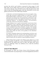
Figure 1 Schematic presentation
of the two different mechanisms
governing charge transport in organic
semiconductors. The so-called hop-
ping transport assumes a thermally
activated hopping between charge-
traps and is always present, the
resulting mobilities are very small.
For certain materials a mechanism
yielding much higher mobilities has
been observed, which is commonly
referred to as “band-like”, thus im-
plying a similarity to band-transport
observed in conventional semicon-
ductors.
XXII Foreword
To reach this frequency is in no way trivial, and in particular requires a mi-
nimum mobility of charge carriers within the organic field effect transistors.
This important issue will be discussed below. It has to be noted, however, that
in view of the technological applications, a reliable and constant device per-
formance may be even more important than a peak performance of the indi-
vidual circuits.
Before we start to address particular properties of organic field effect transis-
tors, or present the limitations and the prospects of improving the performance
of these devices, we would like to point out that the interest in OFETs goes far
beyond solving technological problems. With regard to determining charge
carrier mobilities in organic materials and, more importantly, understanding
the physics behind, in particular, the band-like transport observed in organic
semiconductors, OFETs play a key role in experimentally determining these
parameters. While there are other ways to determine conductivities, charge
carrier mobilities, and temperature dependences in organic materials, for most
of the molecules investigated so far these parameters have been determined us-
ing organic field effect transistors.
The Three Key Aspects of Organic Electronic Devices
With regard to applications as organic semiconductors, there are several
properties of molecular materials that have been improved in the past and
which still need to be optimised further. The most important characteristic of
an organic semiconductor is the charge carrier mobility. The processability of
organic compounds comes second; the question of whether high-performance
thin organic films can be prepared in a straightforward fashion is very impor-
tant not only for technological applications but also for fundamental studies.
Third, the formation of electrical contacts where either electrons or holes
are injected into the organic materials is also critical when it comes to fabricat-
ing a functioning device – for this reason the interaction between organic
molecules and metals is a topic of key interest with regard to the development
of functioning devices. In the following these three main aspects – which are
also the key topic of the articles collected in this book – will by briefly dis-
cussed.
(i) Charge Carrier Mobilities in Organic Semiconductors
Charge carrier mobilities are, as already noted above, a key parameter describ-
ing the performance of a semiconductor. This quantity describes the mobility
of charges, electrons or holes in the presence of an electric field. The most
straightforward way to measure these charge carrier mobilities is to literally
measure the speed of the charge carriers in a semiconductor in the presence of
an electric field. A classical method, which can also be used for organic semi-
conductors, is to excite charge carriers at a defined point in space, e.g. by a la-