- Trang chủ >>
- Khoa Học Tự Nhiên >>
- Vật lý
Polymer assisted synthesis of aligned amorphous silicon nanowires and their core shell structures with au nanoparticles
Bạn đang xem bản rút gọn của tài liệu. Xem và tải ngay bản đầy đủ của tài liệu tại đây (425.54 KB, 5 trang )
Polymer-assisted synthesis of aligned amorphous silicon
nanowires and their core/shell structures with Au nanoparticles
Xing-bin Yan
a,b
, Tao Xu
a
, Shan Xu
a,b
, Gang Chen
a,b
,
Qun-ji Xue
a
, Sheng-rong Yang
a,
*
a
State Key Laboratory of Solid Lubrication, Lanzhou Institute of Chemical Physics, Chinese Academy of Sciences, Lanzhou 730000, China
b
Graduate School of the Chinese Academy of Sciences, Beijing, 100083, China
Received 13 August 2004; in final form 23 August 2004
Available online 11 September 2004
Abstract
Aligned amorphous Si nanowires (SiNWs) were synthesized directly from Si substrates with the assistance of a new carbon-based
network polymer, poly(phenylcarbyne), during the heat-treatment in Ar atmosphere at 1120 °C. A core/shell structure of SiNWs
wrapped with Au nanoparticles was simply fabricated as well. The analytic results of the morphology and microstructure confirmed
the orientation and the amorphous nature of the SiNWs, and the high dispersion of Au nanoparticles on the surface of the SiNWs
without any aggregation. The formation of the SiNWs was explained on the basis of the reaction of carbon with the native silica
layer covering Si substrates.
Ó 2004 Elsevier B.V. All rights reserved.
1. Introduction
Silicon-based nanoscale materials have attracted
much attention in recent years for their valuable semi-
conducting, mechanical, and optical properties, as well
as their potential applications in mesoscopic research
and nanodevices. They are, for example, considered as
candidates for one-dimensional quantum transistor,
composites, and light-emitting diodes [1,2] . Conse-
quently, a great deal of effort has been made in fabricat-
ing Si-based nanostructures, especially silicon nanowires
(SiNWs). Upto now, several methods have been em-
ployed to produce SiNWs, including chemical vapor
deposition (CVD) [3], thermal evaporation of Si powder
[4], metal catalyzed vapor–liquid–solid method [5], laser
ablation [6], oxygen-assisted synthesis [7], heating SiO
2
–
Si mixtures or pure SiO powders [8,9], and solution etch-
ing [10]. Furthermore, it has been recently reported that
enhanced yields of SiNWs are obtained by heating a Si
substrate coated with carbon nanoparticles at 1050 °C
under vacuum [11]. Wherein, the role of carbon is to
react with the oxide probably producing a suboxide-type
species.
Although SiNWs can be mass-produced by the above
methods, it is hard to increase the electrical conductivity
of SiNWs during the growth process. A number of strat-
egies to modify the electronic structure of SiNWs have
been developed, including deposition Ag particles on
SiNWs [12], or formation of metal silicide layers on
SiNWs [13]. This new type of composite SiNWs is
important for the potential applications in future micro-
electronic and optoelectronic devices.
In this communication, we report that aligned amor-
phous SiNWs can be synthesized directly from Si sub-
strates with the assistance of a new carbon-based
network polymer, poly(phenylcarbyne). Moreover, a
core/shell structure of SiNWs wrapped with highly dis-
persed Au nanoparticles is simply fabricated as well.
The methods significantly simplify the preparation of
0009-2614/$ - see front matter Ó 2004 Elsevier B.V. All rights reserved.
doi:10.1016/j.cplett.2004.08.099
*
Corresponding author. Fax: +86 931 8277088.
E-mail address: (S. Yang).
www.elsevier.com/locate/cplett
Chemical Physics Letters 397 (2004) 128–132
aligned SiNWs and the metal–SiNWs composite materi-
als, and make the processes more cost-effective.
2. Experimental
The poly(phenylcarbyne), PPC, was inexpensively
synthesized by the procedure: the reduction of the
appropriate PhCCl
3
monomer, with an ultrasonically
generated emulsion of Na–K alloy and an ethereal sol-
vent, tetrahydrofuran (THF), reported in detail else-
where [14,15]. This polymer is composed of a
randomly constructed network of tetrahedral hybridized
phenylcarbyne units and can be converted into dia-
mond-like carbon by pyrolysis [15]. Freshly prepared
PPC powder was dissolved THF, followed by spin-
coating onto the surfaces of different type single crystal
silicon substrates (10 0) and (1 1 1), respectively, that
sequentially cleaned with deionized water, ethanol, and
acetone, to allow the formation of the polymer film with
the thickness of 200 nm after the removal of the THF by
evaporation at 60 °C. The polymer film on the silicon
substrate was inserted into a quartz tube, heated in an
Ar atmosphere at 10 °C/min to 1120 °C, and held at
1120 °C for 2 h. After this treatment, the targe t amor-
phous SiNWs were obtained.
The freshly prepared SiNWs were peeled off from Si
substrate and dispersed in a solution of HAuCl
4
(10
mL, 0.1 M) with the aid of ultrasonication to give a sus-
pension. The suspension was supersonicated for 30 min,
aged for 1 h, and was gravi ty-filtered and air-dried at
room temperature, respectively. Finally, the SiNWs
wrapped highly dispersed Au nanoparticles were ob-
tained by heating them upto 300 °C at a rate of 5 °C/
min and keeping them at that temperature for 1 h under
Ar atmosphere in a seal pyrolysis quartz tube.
The morphology and structure of nanowires (were
examined by scanning electron microscopy (SEM,
JSM-5600LV), energy dispersive X-ray spectroscopy
(EDX), transmission electron microscopy (TEM, JEM -
1200EX), selected area electron diffraction (SAED),
micro-Raman backscattering spectroscopy (Raman, Jo-
bin Yvon T64000), and X-ray photoelectron spectros-
copy (XPS, Perkin–Elmer PHI-5702).
3. Results and discussion
After pyrolysis of the polymer/Si, a blue tinted gray
colored wool-like film was all deposited on the different
type Si sub strates, which indica tes that the type of Si
substrate does not affect the formation of the SiNWs.
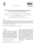
The SEM images in Fig. 1a reveal that the nanowires
(NWs) are highly aligned perpendicular to the Si sub-
strate. As is seen form the cross-sectional view along
the edge of the scratched film, the orientation of the
NWs is widespread over the whole substrate. The homo-
geneous thickne ss of the NWs film is easily obtained to
be about 500 lm. Thus, the growth rate of the NWs is
estimated to be about 70 nm/s. The magnified SEM im-
age in the right inset shows that the NWs appear dense
and parallel to each other. More interestingly, the SEM
images in Fig. 1b reveal some dandelion-like wires. As is
seen form the top view of the NWs film, the relatively
straight nanowire spli ts into several curly sub-branche s
to different orientation. The magnified image in the right
inset shows these sub-branches are similar to wire-like
spherical particle agglomerates with the width range
from nanoscale to micron-scale.
The EDX spectrum of aligned NWs on the cross-
section of the SiNWs film, shown in Fig. 2a, reveals
these NWs are mainly composed Si. The remaining
oxygen peak comes from the surfa ce oxidation of the
nanowires and the atomic rate for Si:O in these nano-
wires is 7:1 on average. While, the ED X spectrum of
particle-linked wires on the tip of SiNWs film, shown
in Fig. 2b, reveals that these wires consist of Si, C and
O, and further quantitative analysis shows that the
atomic ratio for Si:C:O is ca. 1.7:7.3:1, indicating that
these particles are mainly composed carbon, which can
provide evidence for the growth mechanism of the
SiNWs. The possibi lity of the formation amorphous sil-
icon oxide nanowires can be excluded by the following
discussions: first, PPC is a non-oxygenous carbon-based
Fig. 1. SEM images of the SiNWs homogeneously grow on a large area of the Si substrate: (a) cross-sectional view; (b) top view.
X. Yan et al. / Chemical Physics Letters 397 (2004) 128–132 129
network polymer; second, the pyrolysis quartz tube had
been vacuumized before inputting Ar atmosphere; third,
though the Si substrate have thin native oxide layer, it is
too thin (usually less than 1 nm, measured by an ellips-
ometer) to grow silicon oxide nanowires with the thick-
ness of 500 lm.
The low magnification TEM image in Fig. 3a shows
the general morphology of the SiNWs. The diameters
are in the range from several tens to hundreds of nanom-
eters. Most of them are straight and have a smooth sur-
face. Fig. 3b shows a TEM image of individual curly
wire with the average diameter of 400 nm, revealing
the typical structure of wire-like spherical particle
agglomerates at the end of the wire. Fig. 3c shows a
magnified TEM image of a part of individual relatively
straight SiNW with the same diameter. The correspond-
ing highly dispersed selected area electron diffraction
(SAED) pattern reveals its amorphous nature (inset).
Fig. 3d,e show TEM images of the core/shell structure
of the SiNWs wrapped Au nanoparticles. The average
particle size of the wrapped Au nanoparticles in the
composite SiNWs is 5 ± 1.5 nm. It is noted that the
Au nanoparticles are well dispersed on the surface of
the SiNWs without any aggregation. The SAED pattern
(a)
Si
O
Intensity (a.u.)
Intensity (a.u.)
0.0 0.5 1.0 1.5 2.0 2.5 3.0 3.5 4.0
(b)
Si
C
O
Energy (KeV)
0.0 0.5 1.0 1.5 2.0 2.5 3.0 3.5 4.0
Energy (KeV)
Fig. 2. EDX spectra of the aligned nanowires (a) and the particle-linked wires (b).
Fig. 3. (a) Low magnification TEM image of SiNWs; (b) TEM image of a single particle-linked wire; (c) TEM image of a single straight SiNWs and
the corresponding highly dispersed selected area electron diffraction (SAED) pattern; (d) and (e) TEM images of SiNWs wrapped Au nanoparticles
and the corresponding SAED pattern.
130 X. Yan et al. / Chemical Physics Letters 397 (2004) 128–132
in the inset of the TEM image of individual Au–SiNW
shows diffraction rings, which is corresponded to Au
crystal. Moreover, the content of the Au nanoparticles
in the Au–SiNWs is 5 at.%, which is determined by
EDS.
Part of the SiNWs film was peeled off from Si sub-
strate and used to measure the Raman. Two peaks
around 301 and 519 cm
À1
were observed, as is shown
in Fig. 4. It is wel l known that those two Raman peaks
are characteristic of a silicon structure, corresponding to
the second-order transverse acoustic phonon mode
(2TA), and the first-order transverse optical phonon
mode (TO) of silicon, respectively. The Raman result
confirms that the nanowires are composed of silicon.
In order to study the growth mechanism of SiNWs in
our synthesis system, two additional experiments were
carried out under similar conditions: (1) in the absence
of PPC film on Si substrate to verify whether carbon
plays an important role in the formation of the SiNWs;
(2) in the addition of a procedure that Si substrate was
cleaned with aqueous solut ion of 5% HF for 10 min to
remove the native oxide layer, to verify whether the
native oxide layer plays another important role in the
formation of the SiNWs. The above experiential results
show that there is no nanowire existing on the surface of
the Si substrate. It indicates that the polymer film and
the native oxide layer on Si substrate are both necessary
for fabri cating SiNWs.
The PPC polymer has a hydrocarbon network mainly
composed of tetrahedral hybridized carbon atoms, each
bearing one phenyl. Under high temperature of heat-
treatment, phenyl rings and an amount of hydrogen
evolved from the polymer network, resulted in the con-
version of diamond-like carbon phase from polymer
phase [15]. TEM analysis of carbon films prepared by
the heat-treatment of PPC above 600 °C confirmed that
the carbon pha se was composed of small carbon nanopar-
ticles [14]. Moreover, when the temperature is below
1050 °C, the product is amorphous carbon film coated
on Si substrate; when the temperature is 1050–1100 °C,
the surface of the carbon film changes very rough and
there are some erodible taints on Si substrate, which indi-
cates that chemical reaction may take place; when the
temperature is above 1100 °C, aligned amorphous SiNWs
film is main product. Thus, we think that the higher pyro-
lysis temperature (1120 °C) will lead to a large amount of
carbon nanoparticles having high chemical activity. The
growth of SiNWs may start from the reaction of the active
carbon nanoparticles with the native oxide layer on Si
substrate [11,16,17]. This native oxide layer is reduced
by carbon nanoparticles to yield silicon monoxide, and
then the nucleation site of the Si nanostructures is formed
by the decomposition of silicon monoxide. The above
reactions are proposed as below:
Si
x
O
2
! Si
x
O þ CO ðx > 1Þð1Þ
Si
x
O ! Si
xÀ1
þ SiO ð2Þ
2SiO ! Si þ SiO
2
ð3Þ
Finally, aligned SiNWs are grown perpendicular to
the Si substrate at 1120 °C. Moreover, due to the carbon
particles are superfluous compared with native oxide
layer, remnant carbon particles will stay on the top of
the SiNWs and form wire-like spherical particle agglom-
erates, linking with SiNWs. Based on the above discus-
sions, we propose that the formation of the SiNWs
follows the conversion from PPC to carbon particles,
the reduction from native oxide layer to silicon monox-
ide, and the growth of SiNWs, which is schematically
shown in Fig. 5.
The SiNWs are in amorphous state instead of a crys-
talline phase in our synthesis. It may be due to the much
too growth rate (about 70 nm/s). We speculate the
growth rate is so rapid that the Si atoms have no time
to stack themselves into crystalline order. Furthermore,
due to high density of the SiNWs film, the van der Waals
force between nanowires should be large. Thus, this
interaction force plays an important role to keep the
SiNWs grow upward and to be highly oriented [18].
For the formation mechanism of the core/shell struc-
ture of SiNWs wrapped highly dispersed Au nanoparti-
cles, we explain as followed: unde r the ultrasonication,
some AuCl
À
4
anions in the solution of HAuCl
4
are uni-
formly absorbed on the surface of the SiNWs. Because
of the high standard electrode potential of the
Au
3+
/Au
0
couple, Au
3+
has high polarization and high
chemical reactivity. Au
3+
could be easily reduced to
Au
0
in air at 200 °C [19]. Thus, the Au–SiNWs can be
obtained by heat-treatment of the SiNWs and
HAuCl
4
Æ H
2
O at 300 °C in Ar atmosphere. It is believed
that all chlorin have been evaporated during the thermal
200 300 400 500 600 700 800 900
2TA
Intensity (a.u.)
Raman shift (cm
-1
)
TO
Fig. 4. Raman spectrum of the SiNWs scratched off from the
substrate. Two peaks at 302 and 520 cm
À1
were observed which
correspond to 2TA and TO modes of silicon, respectively.
X. Yan et al. / Chemical Physics Letters 397 (2004) 128–132 131
processes, which is confirmed by EDS and XPS analysis
of chlorin.
4. Conclusion
In summary, we have success fully synthesized highly
aligned amorphous SiNWs on a large-area Si substrate
with the assistance of PPC polymer, and simply fabri-
cated SiNWs wrapped highly dispersed Au nanoparti-
cles. In our synthesis system, Si substrate is used as
the source of SiNWs, and the native oxide layer and car-
bon-based network polymer film are crucial for the
growth of SiNWs. We expect that the present method
would be a promising way for a mass -production of
highly aligned SiNWs and their core/shell structures
with metal nanoparticles for the future applications in
microelectronic and optoelectronic dev ices.
Acknowledgements
The authors are grateful to the National Natural
Science Foundation of China (Grant Nos. 50172052,
50375151 and 50323007), 863 program (Grant No.
2003 AA305670) and ÔTop Hundred Talents ProgramÕ
of Chinese Academy of Sciences for financial support.
Appendix A. Supplementary material
Supplementary data associated with this article can
be found, in the online version at doi:10.1016/
j.cplett.2004.08.099.
References
[1] R.S. Wagner, W.C. Ellis, Appl. Phys. Lett. 4 (1964) 89.
[2] A.P. Alivisatos, Science 271 (1996) 933.
[3] X.Y. Zhang, L.D. Zhang, G.W. Meng, G.H. Li, N.Y.J. Phillipp,
F. Phillipp, Adv. Mater. 13 (2001) 1238.
[4] D.P. Yu, Z.G. Bai, Y. Ding, Q.L. Hang, H.Z. Zhang, J.J. Wang,
Y.H. Zou, W. Qian, G.C. Xiong, H.T. Zhou, S.Q. Feng, Appl.
Phys. Lett. 72 (1998) 3458.
[5] M.K. Sunkara, S. Sharma, R. Miranda, G. Lian, E.C. Dickey,
Appl. Phys. Lett. 79 (2001) 1546.
[6] A.M. Morales, C.M. Lieber, Science 279 (1998) 208.
[7] R.Q. Zhang, Y. Lifshitz, S.T. Lee, Adv. Mater. 15 (2003)
635.
[8] J.L. Gole, J.D. Stout, W.L. Rauch, Z.L. Wang, Appl. Phys. Lett.
76 (2000) 2346.
[9] C.P. Li, C.S. Lee, X.L. Ma, N. Wang, R.Q. Zhang, S.T. Lee,
Adv. Mater. 15 (2003) 607.
[10] K.Q. Peng, Z.P. Huang, J. Zhu, Adv. Mater. 16 (2004)
73.
[11] S. Botti, R. Gardi, R. Larciprete, A. Goldoni, L. Gregoratti, B.
Kaulich, A. Govindaraj, C.N.R. Rao, Chem. Phys. Lett. 371
(2003) 394.
[12] X.H. Sun, H.Y. Peng, Y.H. Tang, W.S. Shi, N.B. Wong,
C.S. Lee, S.T. Lee, T.K. Sham, J. Appl. Phys. 89 (2000)
6396.
[13] C.P. Li, N. Wang, S.P. Wong, C.S. Lee, S.T. Lee, Adv. Mater. 14
(2002) 218.
[14] X.B. Yan, T. Xu, X.B. Wang, H.W. Liu, S.R. Yang, Carbon 42
(2004) 232.
[15] G.T. Visscher, D.C. Nesting, J.V. Badding, P.A. Bianconi, Science
260 (1993) 1496.
[16] C.N.R. Rao, G. Gundiah, F.L. Deepak, A. Govindaraj, A.K.
Cheetham, J. Mater. Chem. 14 (2004) 440.
[17] G. Gundiah, F.L. Deepak, A. Govindaraj, C.N.R. Rao, Chem.
Phys. Lett. 381 (2003) 579.
[18] X.H. Chen, Y.J. Xing, J. Xu, J. Xiang, D.P. Yu, Chem. Phys.
Lett. 374 (2003) 626.
[19] H. Kozuka, S. Sakka, Chem. Mater. 5 (1993) 222.
PPC film
Si
x
O
2
film
Si substrate
C film
C particles
Sizeable SiO
SiNWs
Diffusion of Si
Particle-linked wires
Fig. 5. A schematic diagram of the growth mechanism of amorphous SiNWs from Si substrate with the assistance of polymer-converted carbon film.
132 X. Yan et al. / Chemical Physics Letters 397 (2004) 128–132