- Trang chủ >>
- Khoa Học Tự Nhiên >>
- Vật lý
A molecule detector adsorbate induced conductance gap change of ultra thin silicon nanowire
Bạn đang xem bản rút gọn của tài liệu. Xem và tải ngay bản đầy đủ của tài liệu tại đây (330.64 KB, 5 trang )
A molecule detector: Adsorbate induced conductance gap change of ultra-thin
silicon nanowire
Y.H. Zhang
a
, X.Q. Zhang
b
,H.Li
b
, C.A. Taft
a,
*
, G. Paiva
c
a
Centro Brasileiro de pesquisas Físicas, Rua Dr. Xavier Sigaud, 150, 22290 Rio de Janeiro, Brazil
b
Physics Department, Ocean University of China, Qingdao, Shandong 266100, China
c
Departamento de Química Fundamental, Universidade Federal de Pernambuco, Recife, PE 50740-540, Brazil
article info
Article history:
Received 11 November 2008
Accepted for publication 22 January 2009
Available online 30 January 2009
Keywords:
Nanowire
Molecule detector
Electronic transport
Adsorbate
Conductance gap
abstract
Inspired by the work of Lieber and co-workers [F. Patolsky, B.P. Timko, G. Zheng, C.M. Lieber, MRS Bull. 32
(2007) 142], we present a general discussion of the possibility of using atomic-chain scaled Si nanowires
to detect molecules. Surface-modified Si nanowires were optimized by density functional theory (DFT)
calculations. The electronic transport properties of the whole system, including Si nanowires and
adsorbed molecules, sandwiched between two gold electrodes are investigated by means of non-equilib-
rium Green’s function (NEGF) formalism. However, the overall transport properties, including current–
voltage (I–V) and conductance–voltage (G–V) characteristics hardly show adsorbate sensitivity. Interest-
ingly, our results show that the conductance gap clearly varies with the different adsorbates. Therefore
different molecules can cause differences in the conductance gap compared with the bare Si nanowire.
The results provide valuable information regarding the development of atomic-chain scaled molecular
detectors.
Ó 2009 Elsevier B.V. All rights reserved.
1. Introduction
Semiconductor nanowires are emerging as a powerful and gen-
eral class of ultrasensitive, electrical sensors for the direct detec-
tion of biological and chemical species [1]. The similarity in size
of the nanowires and biological and chemical species being sensed
makes nanowires an obvious choice for creating highly sensitive
tools that can probe nanometer-sized systems. Semiconductor
nanowires, moreover, exhibit unique electrical and optical proper-
ties that can be exploited for sensing. These characteristics make
semiconductor nanowires one of the best defined and most versa-
tile nanomaterial systems available today [2].
Lieber and co-workers [1] discussed representative examples of
nanowire nanosensors for ultrasensitive detection of proteins and
individual virus particles as well as recording, stimulation, and
inhibition of neuronal signals in nanowire–neuron hybrid struc-
tures. The concepts underlying these experiments is as follows:
When a single particle binds to a receptor linked to the surface
of a nanowire FET detector, it yields a conductance change due to
the change in surface charge; when the particle subsequently un-
binds, the conductance returns to baseline. We tried to use the
same method to detect molecules using ultra-thin nanowire, how-
ever our results suggest that the overall conductance–voltage
(G–V) characteristic shows only a moderate adsorbate sensitivity.
Fortunately, the conductance gap clearly changes in response to
different adsorbates.
Technological advances in fabrication and characterization at
the nanoscale level have allowed a level of miniaturization to the
extreme scale where the active component of the electronic device
can involve an ultra-thin nanowire or just a single molecule [3–5].
In recent years, upon molecular adsorption, sharp changes of the
conductance and mechanical properties of nanowires have been
observed experimentally [6]. Small molecules or atoms adsorbed
to the surface of a nanowire (that is surface-modified NWs) can
lead to an increase or decrease in the device conductance depend-
ing on the net charge of adsorbed molecules or atoms and the
semiconductor type [1]. The conductivity of an ultra-thin nanowire
can be tuned by chemisorption of appropriate molecules, which
suggests that the sensitive dependence of the conductance on
molecular adsorption may be used for molecular detection [5].
Understanding the adsorbate-induced changes in conductance is
therefore important for the development of nanowire nanosensors.
2. Modeling methods
In an earlier study, we have demonstrated by geometry optimi-
zation calculations that semiconductor materials confined in CNTs
prefer to form well-ordered nanowires [7]. Similarly, the carbon
nanotube served as a mould during the optimization of Si nanowire,
0039-6028/$ - see front matter Ó 2009 Elsevier B.V. All rights reserved.
doi:10.1016/j.susc.2009.01.025
* Corresponding author.
E-mail address: (C.A. Taft).
Surface Science 603 (2009) 847–851
Contents lists available at ScienceDirect
Surface Science
journal homepage: www.elsevier.com/locate/susc
the FORCITE module of MATERIALS STUDIO was used to perform
geometry optimization of Si nanowire embedded in (7, 7) single
wall carbon nanotube, the diameters and the length of the nano-
tube are chosen as 9.49 and 36.8927 Å, respectively. DFT calcula-
tions were used to refine the optimization of the Si nanowire, to
get minimized energy and stable structures of nanowire. The whole
system, including the CNT and Si nanowire, has more electron den-
sity of states and is therefore not sensitive to the adsorbates. There-
fore, only the optimized Si nanowires were used to test the
dependence of electronic transport properties on the adsorbates.
The iterative progress was done and the number of the max itera-
tions was 10
5
. The universal force field was used to model the iter-
ations in the optimization process. To enhance the quality of the
calculation, we defined the energy convergence tolerance as
0.001 kcal/mol and the force convergence tolerance as 0.5 kal/
mol/Å. The atomic coordinates were adjusted until the total energy
of the structure was minimized.
Based on the stable structures of Si nanowires, we performed
DFT [8] calculations to obtain the adsorption of H
2
,H
2
O, O
2
mole-
cules and Fe atoms (Hereafter, in order to simplify, we denoted
them as Si
n
&mX, X= H
2
,H
2
O, O
2
and Fe, where n and m is the num-
ber of the Si atoms and X, respectively). In these optimizations, the
effective core potential (ECP) and a double-numerical basis includ-
ing d-polarization function (DND) are chosen. The density function
is treated with generalized gradient approximation (GGA) with ex-
change-correlation potential parameterized by Wang and Perdew
[9].
The conductance of the NWs depends not only on the intrinsic
properties of the NWs, but also on the electrode materials [10].
To determine the conductance of NWs, one must first bring it into
contact with at least two external electrodes (Fig. 1). Here, we use
gold (111) film as contacts, and the nanowire–electrode contact
distance is constant when the different NWs were put into the
middle of contacts, namely the vertical distance between the end
atoms of the nanowires and the gold contacts is 1.811 Å. The three
gold atoms of Au (11 1) surface connect to both ends of the nano-
wire. The Au–Au bond length is 2.885 Å and the end atom of the
nanowire is equidistant from the three gold atoms.
The electronic transport properties of the optimized Si
11
chain,
Si
11
&9H
2
,Si
11
&9H
2
O, Si
11
&9O
2
and Si
11
&13Fe were calculated by
using non-equilibrium Green’s function (NEGF) formalism under
an applied bias [11]. According to our previous calculation [12],
the self-consistent field is obtained using DFT method from the
standard quantum chemistry software package Gaussian 98 [13].
The whole system is divided into two parts: contact subspace
and nanowire subspace. The contact subspace is treated via a
one-time calculation of the surface Green’s function of the contacts
(Au (11 1) films) including their atomicity and crystalline symme-
try. Different nanowires coupled to the same contacts have differ-
ent couplings, but the contact surface Green’s function is
independent of the nanowire. In the present calculations, the
LANL2DZ [14,15] basis set with relativistic core pseudopotentials
was used to describe the contacts and molecule. The self-consis-
tent potential is calculated using DFT with Becke-3 exchange [16]
and Perdew–Wang 91 correlation [17].
The current through the contact-nanowire-contact system is an
integral of the electron transmission probability over energy,
which is given in Eq. (1) [18].
I ¼
2q
h
Z
1
À1
TðEÞ½f ðE À u
1
ÞÀf ðE À u
2
ÞdE; ð1Þ
where f(E) is the Fermi function, and u
1
and u
2
are the electrochem-
ical potentials in the two contacts. The quantity T(E) appearing in
the current equation (Eq. (1)) is called the transmission function,
which represents the sum of transmission probabilities over all
the energy channels, is obtained from the Green’s function using
the Fisher–Lee formalism [19]:
TðEÞ¼Tr½
C
1
G
C
2
G
y
The Green’s function (G) of the gold–NW system is obtained as
G ¼ðE
1
À H
NT
À
R
1
À
R
2
Þ
À1
An orthogonalized tight-binding model is used to obtain the
nanowire Hamiltonian matrix H
NW
. Here,
C
1
and
C
2
, defined by
C
1;2
¼ ið
R
1;2
À
R
y
1:2
Þ
are the broadening functions arising from the coupling between the
NW and Au electrodes on either end.
R
1
and
R
2
(self-energy func-
tions) [19] represent effective Hamiltonians that take into account
the effect of coupling between the Au electrode and the nanowire
and are defined by
R ¼ C
y
1;2
G
Au
C
1;2
. The coupling matrices C
1,2
are
obtained by a suitable partitioning of the Hamiltonian matrix of
the extended gold–NW–gold system. G
Au
is the Green’s function
of the gold contact and is approximated [20] as a diagonal matrix
in which each element is proportional to the local density of states
(LDOS). Since conduction occurs mostly near the Fermi energy, and
since in the case of gold, the s band dominates near the Fermi sur-
face, the value of the LDOS for the s band of Au at the Fermi energy
was set at the observed value [21] of 0.035 eV/atom per electron
spin.
3. Results and discussion
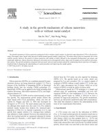
Fig. 2 shows that the snapshots for Si
11
chain, Si
11
&9H
2
,
Si
11
&9H
2
O, Si
11
&9O
2
and Si
11
&13Fe obtained from our atomistic
simulations. Si nanowire is a well-ordered 11-atom double chains
structure that is composed of two parallel single chains in which
the atoms are arranged in a zigzag fashion. 9-H
2
, 9-H
2
O, 9-O
2
and
13-Fe were adsorbed on the Si nanowire, respectively. Especially
interesting, 7-atom and 6-atom Fe features two clusters. Although,
surface reconstruction, chemical passivation, and cross-sectional
geometry of nanowires may have an effect on the electronic trans-
Fig. 1. Schematic representation of the contact-nanowire-contact system.
Fig. 2. (a) Snapshots of Si
11
chain, (b) Si
11
&9H
2
(c) Si
11
&9H
2
O (d) Si
11
&9O
2
(e)
Si
11
&13Fe obtained from our calculations.
848 Y.H. Zhang et al. /Surface Science 603 (2009) 847–851
port properties [22–24], we exclude such factors and concentrate
on the adsorbate effect on the electronic transport of Si nanowires.
Several semi-empirical theories and first-principles methods
have been used to calculate the I–V and G–V characteristics of mol-
ecules and which agree well with experimental results [25]. Typi-
cally the first-principles methods are computationally very
expensive. So in this work, the transport characteristics are calcu-
lated by using a straightforward (computationally inexpensive) yet
rigorous and self-consistent procedure developed by Datta and co-
workers [25]. The optimized Si NWs adsorbed molecules and
atoms were chosen. In order to study the interaction between Si
NWs and gold electrodes, finite gold atoms are chosen to compose
gold clusters to simulate connection between electrodes and NWs.
The electrodes are assumed to be essentially unperturbed relative
to the surface of a bulk metal, and this assumption is clearly not
true for a few atoms near the molecule–metal interface. Therefore
in the electronic transport calculations the Si nanowire is defined
to include two gold clusters from the surface of the electrodes.
The most fundamental quantity that describes the electrical
properties of a bulk material is conductivity, based on which mate-
rials are often divided into conductors, insulators and semiconduc-
tors. Conductivity is defined as
r
=(I/V) Â L/A, where I is the
electrical current, V is the applied bias voltage, L is the length
and A is the cross-sectional area of the material. For a nonmaterial,
A and L are difficult to define precisely, and a more well-defined
quantity is the conductance, G, given by G = I/V.
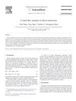
Fig. 3 shows the current–voltage (I–V) and conductance–voltage
(G–V) curves for these five kinds of NWs, respectively. In the fol-
lowing, we will discuss the current–voltage (I–V) and conduc-
tance–voltage (G–V) characteristics of Si NWs.
The I–V characteristics of nanowires are strongly influenced by
three factors: the location of equilibrium Fermi energy E
F
, the po-
tential profile across the nanowire under an applied bias and the
coupling between the nanowire and the electrodes. Voltage profile
across the conductor is a very important factor in determining the
I–V characteristics. An applied voltage is known to drop largely
across the metal–molecule interface, leading to a weaker drop in
the molecule. At equilibrium, the entire system has a common Fer-
mi energy E
F
which is equal to the electrochemical potentials
l
1
and
l
2
in the two contacts. When we apply a voltage V
appl
across
the structure we cause
l
1
and
l
2
to split by eV
appl
:
l
1
À
l
2
= eV
appl
.
Of course, we can choose freely any reference for the zero of our
applied potential. For example, we could take contact 1 as our ref-
erence and write:
l
1
= E
F
and
l
2
= E
F
+ eV
appl
. However, we also
have to take into account the shifting of the molecular levels,
which depends on the detailed shape of the potential profile inside
the molecule. Here, we introduce the average potential <d
t
mol
(r)>
inside the molecule due to the applied bias, namely <d
t
mol
(r)> =
g
e-
V
appl
, where the voltage division factor
g
is a number between 0
and 1 (detailed discussion in Ref. [25]). The precise nature of the
potential profile is an important input to semi-empirical calcula-
tions of transport. Tian et al. [26] suggested using a flat potential
profile inside the molecule, with a voltage division factor describ-
ing its position. Such a flat profile was obtained by Mujica et al.
[27] by solving a 1-D Poisson equation, and experimentally mea-
sured for longer (
l
$m) wires by Seshadri and Frisbie [28]. How-
ever, in all these cases the geometry under consideration is a
series of 2-D charge sheets with potential variations only along
the wire axis. The 1-D Poisson equation allows variations only
along one coordinate, while the measurements in Ref. [28] referred
to a self-assembled monolayer (SAM) where once again transverse
potential variations are screened out by the presence of neighbor-
ing molecules. In contrast, Lang and Avouris [29] obtained a signif-
icant potential drop in a carbon atomic wire, which is a
consequence of fields penetrating from transverse directions, as
correctly predicted for break-junction geometry by a 3-D Poisson
equation. Our particular geometry is suited to the break-junction,
since the Hartree term in Gaussian 98 is calculated for a 3-D geom-
etry. It is noted that the voltage drop across the device itself is
smaller than the applied voltage bias owing to screening effects,
incorporated self-consistently through the Hartree term of our
Fock matrix.
Current–voltage (I–V) curves obtained from our calculations are
shown in Fig. 3a. It is clear that the I–V curves of all absorbate Si
NWs do not follow an Ohmic pattern. Linear current–voltage (I–
V) characteristics under a low and high applied bias and nonlinear
current–voltage (I–V) characteristics under a definite applied bias
are found. These interesting properties have made them the focus
of intensive research. Larade and his co-workers have performed
first-principles analysis of the transport properties of carbon atom-
ic wires in contact with two metallic electrodes under external bias
[22]. They found that the low-bias current–voltage (I–V) character-
istic is linear. The linear region is corresponding to the conduc-
tance gap, which is caused by finite-size effects.
The conductance of a molecule depends on the alignment of the
molecular energy levels, especially the highest occupied molecular
orbital (HOMO) and lowest occupied molecular orbital (LUMO),
relative to the Fermi levels of the electrodes. Typically, the Fermi
level is positioned in the LUMO–HOMO gap of the molecule
because if the HOMO or LUMO is close to the Fermi level of an
electrode, electrons transfer between the molecule and the elec-
-8 -6 -4 -2 0 2 4 6 8
-40
-30
-20
-10
0
10
20
30
40
Si11 chain
Si11&9H
2
Si11&9H
2
O
Si11&9O
2
Si11&13Fe
Current (µA
Applied Bias (V)
-8 -6 -4 -2 0 2 4 6 8
0
5
10
15
20
25
Si11 chain
Si11&9H
2
Si11&9H
2
O
Si11&9O
2
Si11&13Fe
dI/dV (mA/V)
A
pp
lied Bias (V)
7.2
6.77
6.63
6.20
5.86
a
b
Fig. 3. (a) Current–voltage curves and (b) conductance spectra of Si
11
chain,
Si
11
&9H
2
,Si
11
&9H
2
O, Si
11
&9O
2
and Si
11
&13Fe.
Y.H. Zhang et al. /Surface Science 603 (2009) 847–851
849
trode, and consequently the molecules are oxidized or reduced
spontaneously. When the LUMO or HOMO is brought close to the
Fermi levels, electrochemical oxidation or reduction occurs. For
molecules that can be reversibly oxidized or reduced, significant
changes in the conductance occur. The energy-level alignment is
determined by the intrinsic properties of the molecule and the
electrodes, and also by the interactions between the molecule
and the two electrodes, which are often difficult to determine for
both theory and experiment [30,31].
The first example of electrical detection of proteins in solution
using nanostructures was reported by Lieber’s group using single
p-type silicon nanowrire devices in 2001 [32]. They developed
the use of nanowire devices for the detection of multiple disease
marker proteins simultaneously in a single versatile detection plat-
form [33]. Compared with Lieber and co-workers’ work [1], they
mainly distinguish the absorbed biological species according to
the conductance; here, we find that we can use the conductance
gap to distinguish the absorbed molecules.
From Fig. 3b, we observe that there are many peaks and valleys
in the G –V curves. The linear region in I–V curve is corresponding
to the conductance gap in G–V curve, and when the external ap-
plied bias is zero or small, every I–V curve exhibits a linear region
every, and G–V curve exhibits a conductance gap. It is difficult to
obtain any rule from the whole I–V or G–V curves, so it seems that
we can not detect the molecules using these nanowires. However,
it is obviously that the conductance gaps are different when the
molecules are different, so we can detect according to this prop-
erty. Si NWs absorbed molecules make conductance gap narrow.
However, especially interesting, the conductance gap increase for
Si NWs absorbed Fe atoms clusters, which make it possible to de-
tect the molecules.
Underlying detection using semiconductor nanowires is their
configuration as field-effect transistors (FETs), which exhibit a con-
ductivity change in response to variations in the electric field or
potential at the surface of the device [1]. In a standard FET, the con-
ductance of the semiconductor between the source and drain is
modulated between on and off states by a third gate electrode cou-
pled through a thin dielectric layer to the semiconductor. Applying
a gate voltage leads to an increase/decrease in conductance. The
binding of molecules to a nanowire is analogous to applying a volt-
age using a gate electrode. Fig. 3b shows differential conductance
as a function of bias voltage. It becomes complex to identify the
molecules from the overview of the G–V curves. The increase, de-
crease and the positions of peaks of the G–V curves show only
moderate adsorbate sensitivity. Interestingly, the width of the con-
ductance gap clearly changes with the difference of the adsorbates.
We observe wide gaps in the G–V
curves when the applied bias is
very
low
or zero, which is due to the energy gap between HOMO
and LUMO. Above a given threshold bias, the conductance sud-
denly increases to the first peak as shown in Fig. 3b.
Fig. 4 shows the zero bias transmission through NWs absorbed
molecules and atoms and corresponding to the densities of states
(DOSs) of these absorbate nanowires near the Fermi energy. Zero
bias transmission is the electronic transmission probability at zero
or very low applied bias. It is the probability for electrons transmit-
ting form one electrode to the other, not the real electron transmis-
sion. Under a relatively higher bias, the electrons will transmit
through the channels according to Eq. (1) which is related to trans-
mission probability and applied bias. Very high bias can shift the
zero bias transmission a bit, and then the electron transmission
will be according to the shifted transmission probability. From
Fig. 4a, we can see that all the transmission curves exhibit low re-
gions around Fermi energy which are due to their energy gap be-
tween HOMO and LUMO. The Fermi energy is located at 11 eV,
which is inside the HOMO–LUMO gap. The transmission is
observed to be low around the Fermi level. Under and above the
Fermi level, there are two energy regions which contribute signif-
icantly to the transmission. The first region mainly comes from the
highest occupied molecular orbital (HOMO) contribution. The sec-
ond region mainly comes from the lowest unoccupied molecular
orbital (LUMO) contribution. We call it HOMO (LUMO) transmis-
sion region. Electronic densities, namely DOSs result in the differ-
ence of the conductance spectra, which are corresponding to
Fig. 3b.
The interaction between H
2
,O
2
,H
2
O, Fe and the Si atomic chain
leads to rearrangement of the electrons in the system which
remarkably influences the transmission of the Si atomic chain.
The middle part of the Si atomic chain is covered by the molecules
or atoms, which causes a sharp change in the transmission. The
numbers of DOSs are in the order of the Si
11
chain, Si
11
&9H
2
,
Si
11
&9H
2
O, Si
11
&9O
2
and Si
11
&13Fe from small to large, which cor-
responds to the conductance order.
The conductance gap has been demonstrated by many previous
works both experimentally [34] and theoretically [35,36]. In this
work, we mainly focus on how its conductance gap depends on
the adsorbates of the Si nanowires. Here we observe wide conduc-
tance gaps in the G–V curves, which can be ascribed to Coulomb
blockade phenomena. In general, Coulomb blockade occurs when
a confined electronic system (the nanowire in our simulation) is
weakly coupled to source and drain electrodes [37]. At low-bias,
nonresonant tunneling is the dominant transport mechanism.
When the bias voltage applied is sufficient to align an energy level
-16 -14 -12 -10 -8 -6
-5
-4
-3
-2
-1
0
Si11 chain
Si11&9H
2
Si11&9H
2
O
Si11&9O
2
Si11&13Fe
-16.0 -15.5 -15.0 -14.5
-4
-3
-2
-1
0
10
10
10
10
10
10
10
10
10
10
10
Transimission
Energy, E (eV)
-16-14-12-10 -8 -6
0
40
80
120
160
200
240
Si11 chain
Si11&9H
2
Si11&9H
2
O
Si11&9O
2
Si11&13Fe
Density of states (1/eV)
Ener
gy
, E (eV)
a
b
Fig. 4. (a) Transmission function and (b) the density of states of Si
11
chain,
Si
11
&9H
2
,Si
11
&9H
2
O, Si
11
&9O
2
,Si
11
&13Fe. The dashed line is the Fermi energy.
850 Y.H. Zhang et al. /Surface Science 603 (2009) 847–851
of the nanowire with the Fermi level of an electrode, resonant
transport commences and the Coulomb blockade is lifted. The bias
voltage required to initiate resonant transport thus defines the
conductance gap of the device. The conductance gap changes with
the difference of the adsorbates. The adsorbates control the con-
ductance gap as the third terminal in FET. In our devices, the Si
nanowire incorporated with adsorbate molecules, coupled to two
gold electrodes, act as a confined electronic system. Although,
our device has only two terminals without a gate electrode, the
conductance gap in Fig. 3b shows a fluctuation. The adsorbate mol-
ecules likely act as local charge defects resulting in the stochastic
gating.
4. Conclusion
In summary, optimized Si NWs and Si NWs adsorbed different
molecules (H
2
,H
2
O and O
2
) have been obtained by DFT calcula-
tions. We also investigated the electronic transport properties of
silicon nanowires without and with adsorbate molecules using
non-equilibrium Green’s function (NEGF) formalism. Because of
the presence of the adsorbate molecules, all of the electronic trans-
port properties of the nanowires are in principle different. How-
ever it becomes difficult to identify molecules from the overview
of G–V curves. Our simulation results indicate that the conductance
gap changes in response to different adsorbates. It is thus possible
that Si nanowires could be used as nanosensors for molecular
detection by measuring the change of the conductance gap.
Acknowledgements
This work was support by National Natural Science Foundation
of China: Grant No. JQ200817.
References
[1] F. Patolsky, B.P. Timko, G. Zheng, C.M. Lieber, MRS Bull. 32 (2007) 142.
[2] F. Patolsky, C.M. Lieber, Mater. Today 8 (2005) 20–28.
[3] G. Cuniberti, G. Fagas, K. Richter, Introducing Molecular Electronics, Springer,
Berlin, 2005.
[4] H.S. Park, C.J. Ji, Acta Mater. 54 (2006) 2645.
[5] H. Li, X.Q. Zhang, Phys. Lett. A 372 (2008) 4294.
[6] Andrew B. Greytak, Carl J. Barrelet, Yat Li, Charles M. Lieber, Appl. Phys. Lett. 87
(2005) 151103.
[7] (a) Y.H. Zhang, J. Meng, X.Q. Zhang, Hui Li, C.A. Taft, Int. J. Quantum. Chem.
109, in press.
(b) X.Q. Zhang, H. Li, K.M. Liew, J. Appl. Phys. 102 (2007) 073709.
[8] DMOL3 is a density functional theory (DFT) program from Materials Studio
distributed by Accelrys, Inc. B. Delley, J. Chem. Phys. 92 (1990) 508.
[9] Y. Wang, J.P. Perdew, Phys. Rev. B 43 (1911) 8911.
[10] F. Chen, J. Hihath, Z.F. Huang, X.L. Li, N.J. Tao, Annu. Rev. Phys. Chem. 58 (2007)
535.
[11] F. Zahid, M. Paulsson, S. Datta, in: H. Morkc (Ed.), Electrical Conduction
Through Molecules, Academic Press, New York, 2003.
[12] H. Li, X.Q. Zhang, J.X. Zhang, X.F. Liu, X.F. Bian, J. Phys. Chem. B 112 (2008)
15588.
[13] Gaussian 98 (Revision A.7), M.J. Frisch, G.W. Trucks, H.B. Schlegel, G.E.
Scuseria, M.A. Robb, J.R. Cheeseman, V.G. Zakrzewski, J.A. Montgomery Jr.,
R.E. Stratmann, J. Burant, C.S. Dapprich, J.M. Millam, A.D. Daniels, K.N. Kudin,
M.C. Strain, O. Farkas, J. Tomasi, V. Barone, M. Cossi, R. Cammi, B. Mennucci, C.
Pomelli, C. Adamo, S. Clifford, J. Ochterski, G.A. Petersson, P.Y. Ayala, Q. Cui, K.
Morokuma, D.K. Malick, A.D. Rabuck, K. Raghavachari, J.B. Foresman, J.
Cioslowski, J.V. Ortiz, A.G. Baboul, B.B. Stefanov, G. Liu, A. Liashenko, P.
Piskorz, I. Komaromi, R. Gomperts, R.L. Martin, D.J. Fox, T. Keith, M.A. Al-
Laham, C.Y. Peng, A. Nanayakkara, C. Gonzalez, M. Challacombe, P.M.W. Gill,
B.G. Johnson, W. Chen, M.W. Wong, J.L. Andres, M. Head-Gordon, E.S. Replogle,
J.A. Pople, Gaussian Inc., Pittsburgh, PA, 1998.
[14] P. Hay, W. Wadt, J. Chem. Phys. 82 (1985) 270.
[15] P. Hay, W. Wadt, J. Chem. Phys. 82 (1985) 284.
[16] A.D. Becke, J. Chem. Phys. 98 (1993) 5648.
[17] J.P. Perdew, in: P. Ziesche, H. Eschrig (Eds.), Electronic Structure of Solids,
Akademic Verlag, Berlin, 1991, p. 11.
[18] S. Datta, Quantum Transport: Atom to Transistor, Cambridge University Press,
Cambridge, 2005.
[19] S. Datta, Electronic Transport in Mesoscopic Systems, Cambridge University
Press, Cambridge, UK, 1995.
[20] W. Tian, S. Datta, S. Hong, R. Reiferberger, J.I. Henderson, C.P. Kubiak, J. Chem.
Phys. 109 (1998) 2874.
[21] D.A. Papaconstantopoulos, Handbook of the Band Structure of Elemental
Solids, Plenum, New York, 1986.
[22] B. Larade, J. Taylor, H. Mehrez, H. Guo, Phys. Rev. B 64 (2001) 075420.
[23] J. Taylor, H. Guo, J. Wang, Phys. Rev. B 63 (2001) 245407.
[24] Yam C. Ma, X. Wang, G. Chen, Appl. Phys. Lett. 85 (2004) 4484.
[25] P. Damle, A.W. Ghosh, S. Datta, Chem. Phys. 281 (2002) 171.
[26] W. Tian, S. Datta, S. Hong, R. Reifenberger, J.I. Henderson, C. Kubiak, J. Chem.
Phys. 109 (1997) 2874.
[27] V. Mujica, A. Roitberg, M. Ratner, J. Chem. Phys. 112 (2000) 6834.
[28] K. Seshadri, C. Frisbie, Appl. Phys. Lett. 78 (2001) 993.
[29] N. Lang, P. Avouris, Phys. Rev. Lett. 84 (2000) 358.
[30] Y. Xue, S. Datta, M.A. Ratner, J. Chem. Phys. 115 (2001) 4292.
[31] G. Heimel, L. Romaner, J L. Brédas, E. Aojer, Phys. Rev. Lett. 96 (2006) 196806.
[32] Y. Cui, Q. Wei, H. Park, C.M. Lieber, Science 293 (2001) 1289.
[33] G. Zheng, F. Patolsky, Y. Cui, W.U. Wang, C.M. Lieber, Nat. Biotechnol. 23 (2005)
1294.
[34] H. Yu, L.J. Webb, J.R. Heath, N.S. Lewis, Appl. Phys. Lett. 88 (2006) 252111.
[35] H. Li, X.Q. Zhang, K.M. Liew, J. Chem. Phys. 128 (2008) 034707.
[36] T. Rakshit, G. Liang, A.W. Ghosh, S. Datta, Nano Lett. 4 (2004) 1803.
[37] Lam H. Yu, Christopher D. Zangmeister, James G. Kushmerick, Nano Lett. 6
(2006) 2515.
Y.H. Zhang et al. /Surface Science 603 (2009) 847–851
851