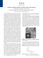
- Trang chủ >>
- Khoa Học Tự Nhiên >>
- Vật lý
optical properties of solids
Bạn đang xem bản rút gọn của tài liệu. Xem và tải ngay bản đầy đủ của tài liệu tại đây (1.69 MB, 198 trang )
SOLID STATE PHYSICS
PART II
Optical Properties of Solids
M. S. Dresselhaus
1
Contents
1 Review of Fundamental Relations for Optical Phenomena 1
1.1 Introductory Remarks on Optical Probes . . . . . . . . . . . . . . . . . . . 1
1.2 The Complex dielectric function and the complex optical conductivity . . . 2
1.3 Relation of Complex Dielectric Function to Observables . . . . . . . . . . . 4
1.4 Units for Frequency Measurements . . . . . . . . . . . . . . . . . . . . . . . 7
2 Drude Theory–Free Carrier Contribution to the Optical Properties 8
2.1 The Free Carrier Contribution . . . . . . . . . . . . . . . . . . . . . . . . . 8
2.2 Low Frequency Response: ωτ 1 . . . . . . . . . . . . . . . . . . . . . . . 10
2.3 High Frequency Response; ωτ 1 . . . . . . . . . . . . . . . . . . . . . . . 11
2.4 The Plasma Frequency . . . . . . . . . . . . . . . . . . . . . . . . . . . . . . 11
3 Interband Transitions 15
3.1 The Interband Transition Process . . . . . . . . . . . . . . . . . . . . . . . . 15
3.1.1 Insulators . . . . . . . . . . . . . . . . . . . . . . . . . . . . . . . . . 19
3.1.2 Semiconductors . . . . . . . . . . . . . . . . . . . . . . . . . . . . . . 19
3.1.3 Metals . . . . . . . . . . . . . . . . . . . . . . . . . . . . . . . . . . . 19
3.2 Form of the Hamiltonian in an Electromagnetic Field . . . . . . . . . . . . . 20
3.3 Relation between Momentum Matrix Elements and the Effective Mass . . . 21
3.4 Spin-Orbit Interaction in Solids . . . . . . . . . . . . . . . . . . . . . . . . . 23
4 The Joint Density of States and Critical Points 27
4.1 The Joint Density of States . . . . . . . . . . . . . . . . . . . . . . . . . . . 27
4.2 Critical Points . . . . . . . . . . . . . . . . . . . . . . . . . . . . . . . . . . 30
5 Absorption of Light in Solids 36
5.1 The Absorption Coefficient . . . . . . . . . . . . . . . . . . . . . . . . . . . 36
5.2 Free Carrier Absorption in Semiconductors . . . . . . . . . . . . . . . . . . 37
5.3 Free Carrier Absorption in Metals . . . . . . . . . . . . . . . . . . . . . . . 38
5.4 Direct Interband Transitions . . . . . . . . . . . . . . . . . . . . . . . . . . 41
5.4.1 Temperature Dependence of E
g
. . . . . . . . . . . . . . . . . . . . . 46
5.4.2 Dependence of Absorption Edge on Fermi Energy . . . . . . . . . . . 46
5.4.3 Dependence of Absorption Edge on Applied Electric Field . . . . . . 47
5.5 Conservation of Crystal Momentum in Direct Optical Transitions . . . . . . 47
5.6 Indirect Interband Transitions . . . . . . . . . . . . . . . . . . . . . . . . . . 50
2
6 Optical Properties of Solids Over a Wide Frequency Range 57
6.1 Kramers–Kronig Relations . . . . . . . . . . . . . . . . . . . . . . . . . . . . 57
6.2 Optical Properties and Band Structure . . . . . . . . . . . . . . . . . . . . . 62
6.3 Modulated Reflectivity Experiments . . . . . . . . . . . . . . . . . . . . . . 64
6.4 Ellipsometry and Measurement of Optical Constants . . . . . . . . . . . . . 71
7 Impurities and Excitons 73
7.1 Impurity Level Spectroscopy . . . . . . . . . . . . . . . . . . . . . . . . . . . 73
7.2 Shallow Impurity Levels . . . . . . . . . . . . . . . . . . . . . . . . . . . . . 73
7.3 Departures from the Hydrogenic Model . . . . . . . . . . . . . . . . . . . . 77
7.4 Vacancies, Color Centers and Interstitials . . . . . . . . . . . . . . . . . . . 79
7.5 Spectroscopy of Excitons . . . . . . . . . . . . . . . . . . . . . . . . . . . . . 83
7.6 Classification of Excitons . . . . . . . . . . . . . . . . . . . . . . . . . . . . 87
7.7 Optical Transitions in Quantum Well Structures . . . . . . . . . . . . . . . 91
8 Luminescence and Photoconductivity 97
8.1 Classification of Luminescence Processes . . . . . . . . . . . . . . . . . . . . 97
8.2 Emission and Absorption . . . . . . . . . . . . . . . . . . . . . . . . . . . . 98
8.3 Photoconductivity . . . . . . . . . . . . . . . . . . . . . . . . . . . . . . . . 104
10 Optical Study of Lattice Vibrations 108
10.1 Lattice Vibrations in Semiconductors . . . . . . . . . . . . . . . . . . . . . . 108
10.1.1 General Considerations . . . . . . . . . . . . . . . . . . . . . . . . . 108
10.2 Dielectric Constant and Polarizability . . . . . . . . . . . . . . . . . . . . . 110
10.3 Polariton Dispersion Relations . . . . . . . . . . . . . . . . . . . . . . . . . 112
10.4 Light Scattering . . . . . . . . . . . . . . . . . . . . . . . . . . . . . . . . . 121
10.5 Feynman Diagrams for Light Scattering . . . . . . . . . . . . . . . . . . . . 126
10.6 Raman Spectra in Quantum Wells and Superlattices . . . . . . . . . . . . . 128
11 Non-Linear Optics 132
11.1 Introductory Comments . . . . . . . . . . . . . . . . . . . . . . . . . . . . . 132
11.2 Second Harmonic Generation . . . . . . . . . . . . . . . . . . . . . . . . . . 134
11.2.1 Parametric Oscillation . . . . . . . . . . . . . . . . . . . . . . . . . . 135
11.2.2 Frequency Conversion . . . . . . . . . . . . . . . . . . . . . . . . . . 136
12 Electron Spectroscopy and Surface Science 137
12.1 Photoemission Electron Spectroscopy . . . . . . . . . . . . . . . . . . . . . . 137
12.1.1 Introduction . . . . . . . . . . . . . . . . . . . . . . . . . . . . . . . 137
12.1.2 Energy Distribution Curves . . . . . . . . . . . . . . . . . . . . . . . 141
12.1.3 Angle Resolved Photoelectron Spectroscopy . . . . . . . . . . . . . . 144
12.1.4 Synchrotron Radiation Sources . . . . . . . . . . . . . . . . . . . . . 144
12.2 Surface Science . . . . . . . . . . . . . . . . . . . . . . . . . . . . . . . . . . 146
12.2.1 Introduction . . . . . . . . . . . . . . . . . . . . . . . . . . . . . . . 146
12.2.2 Electron Diffraction . . . . . . . . . . . . . . . . . . . . . . . . . . . 147
12.2.3 Electron Energy Loss Spectroscopy, EELS . . . . . . . . . . . . . . . 152
12.2.4 Auger Electron Spectroscopy (AES) . . . . . . . . . . . . . . . . . . 153
12.2.5 EXAFS . . . . . . . . . . . . . . . . . . . . . . . . . . . . . . . . . . 154
3
12.2.6 Scanning Tunneling Microscopy . . . . . . . . . . . . . . . . . . . . . 156
13 Amorphous Semiconductors 165
13.1 Introduction . . . . . . . . . . . . . . . . . . . . . . . . . . . . . . . . . . . . 165
13.1.1 Structure of Amorphous Semiconductors . . . . . . . . . . . . . . . . 166
13.1.2 Electronic States . . . . . . . . . . . . . . . . . . . . . . . . . . . . . 167
13.1.3 Optical Properties . . . . . . . . . . . . . . . . . . . . . . . . . . . . 173
13.1.4 Transport Properties . . . . . . . . . . . . . . . . . . . . . . . . . . . 175
13.1.5 Applications of Amorphous Semiconductors . . . . . . . . . . . . . . 175
13.2 Amorphous Semiconductor Superlattices . . . . . . . . . . . . . . . . . . . . 176
A Time Dependent Perturbation Theory 179
A.1 General Formulation . . . . . . . . . . . . . . . . . . . . . . . . . . . . . . . 179
A.2 Fermi Golden Rule . . . . . . . . . . . . . . . . . . . . . . . . . . . . . . . . 183
A.3 Time Dependent 2nd Order Perturbation Theory . . . . . . . . . . . . . . . 184
B Harmonic Oscillators, Phonons, and the Electron-Phonon Interaction 186
B.1 Harmonic Oscillators . . . . . . . . . . . . . . . . . . . . . . . . . . . . . . . 186
B.2 Phonons . . . . . . . . . . . . . . . . . . . . . . . . . . . . . . . . . . . . . . 188
B.3 Phonons in 3D Crystals . . . . . . . . . . . . . . . . . . . . . . . . . . . . . 189
B.4 Electron-Phonon Interaction . . . . . . . . . . . . . . . . . . . . . . . . . . . 192
4
Chapter 1
Review of Fundamental Relations
for Optical Phenomena
References:
• G. Bekefi and A.H. Barrett, Electromagnetic Vibrations Waves and Radiation, MIT
Press, Cambridge, MA
• J.D. Jackson, Classical Electrodynamics, Wiley, New York, 1975
• Bassani and Pastori–Parravicini, Electronic States and Optical Transitions in Solids,
Pergamon Press, NY (1975).
• Yu and Cardona, Fundamentals of Semiconductors, Springer Verlag (1996)
1.1 Introductory Remarks on Optical Probes
The optical properties of solids provide an important tool for studying energy band struc-
ture, impurity levels, excitons, localized defects, lattice vibrations, and certain magnetic
excitations. In such experiments, we measure some observable, such as reflectivity, trans-
mission, absorption, ellipsometry or light scattering; from these measurements we deduce
the dielectric function ε(ω), the optical conductivity σ(ω), or the fundamental excitation
frequencies. It is the frequency-dependent complex dielectric function ε(ω) or the complex
conductivity σ(ω), which is directly related to the energy band structure of solids.
The central question is the relationship between experimental observations and the
electronic energy levels (energy bands) of the solid. In the infrared photon energy region,
information on the phonon branches is obtained. These issues are the major concern of
Part II of this course.
1
1.2 The Complex dielectric function and the complex optical
conductivity
The complex dielectric function and complex optical conductivity are introduced through
Maxwell’s equations (c.g.s. units)
∇ ×
H −
1
c
∂
D
∂t
=
4π
c
j (1.1)
∇ ×
E +
1
c
∂
B
∂t
= 0 (1.2)
∇ ·
D = 0 (1.3)
∇ ·
B = 0 (1.4)
where we have assumed that the charge density is zero.
The constitutive equations are written as:
D = ε
E (1.5)
B = µ
H (1.6)
j = σ
E (1.7)
Equation 1.5 defines the quantity ε from which the concept of the complex dielectric func-
tion will be developed. When we discuss non–linear optics (see Chapter 11), these linear
constitutive equations (Eqs. 1.5–1.7) must be generalized to include higher order terms in
E
E and
E
E
E. From Maxwell’s equations and the constitutive equations, we obtain a wave
equation for the field variables
E and
H:
∇
2
E =
εµ
c
2
∂
2
E
∂t
2
+
4πσµ
c
2
∂
E
∂t
(1.8)
and
∇
2
H =
εµ
c
2
∂
2
H
∂t
2
+
4πσµ
c
2
∂
H
∂t
. (1.9)
For optical fields, we must look for a sinusoidal solution to Eqs. 1.8 and 1.9
E =
E
0
e
i(
K·r−ωt)
(1.10)
where
K is a complex propagation constant and ω is the frequency of the light. A solution
similar to Eq. 1.10 is obtained for the
H field. The real part of
K can be identified as a
wave vector, while the imaginary part of
K accounts for attenuation of the wave inside the
solid. Substitution of the plane wave solution Eq. 1.10 into the wave equation Eq. 1.8 yields
the following relation for K:
−K
2
= −
εµω
2
c
2
−
4πiσµω
c
2
. (1.11)
If there were no losses (or attenuation), K would be equal to
K
0
=
ω
c
√
εµ (1.12)
2
and would be real, but since there are losses we write
K =
ω
c
√
ε
complex
µ (1.13)
where we have defined the complex dielectric function as
ε
complex
= ε +
4πiσ
ω
= ε
1
+ iε
2
. (1.14)
As shown in Eq. 1.14 it is customary to write ε
1
and ε
2
for the real and imaginary parts of
ε
complex
. From the definition in Eq. 1.14 it also follows that
ε
complex
=
4πi
ω
σ +
εω
4πi
=
4πi
ω
σ
complex
, (1.15)
where we define the complex conductivity σ
complex
as:
σ
complex
= σ +
εω
4πi
(1.16)
Now that we have defined the complex dielectric function ε
complex
and the complex
conductivity σ
complex
, we will relate these quantities in two ways:
1. to observables such as the reflectivity which we measure in the laboratory,
2. to properties of the solid such as the carrier density, relaxation time, effective masses,
energy band gaps, etc.
After substitution for K in Eq. 1.10, the solution Eq. 1.11 to the wave equation (Eq. 1.8)
yields a plane wave
E(z, t) =
E
0
e
−iωt
exp
i
ωz
c
√
εµ
1 +
4πiσ
εω
. (1.17)
For the wave propagating in vacuum (ε = 1, µ = 1, σ = 0), Eq. 1.17 reduces to a simple plane
wave solution, while if the wave is propagating in a medium of finite electrical conductivity,
the amplitude of the wave exponentially decays over a characteristic distance δ given by
δ =
c
ω
˜
N
2
(ω)
=
c
ω
˜
k(ω)
(1.18)
where δ is called the optical skin depth, and
˜
k is the imaginary part of the complex index
of refraction (also called the extinction coefficient)
˜
N(ω) =
√
µε
complex
=
εµ
1 +
4πiσ
εω
= ˜n(ω) + i
˜
k(ω). (1.19)
This means that the intensity of the electric field, |E|
2
, falls off to 1/e of its value at the
surface in a distance
1
α
abs
=
c
2ω
˜
k(ω)
(1.20)
3
where α
abs
(ω) is the absorption coefficient for the solid at frequency ω.
Since light is described by a transverse wave, there are two possible orthogonal direc-
tions for the
E vector in a plane normal to the propagation direction and these directions
determine the polarization of the light. For cubic materials, the index of refraction is the
same along the two transverse directions. However, for anisotropic media, the indices of
refraction may be different for the two polarization directions, as is further discussed in
§2.1.
1.3 Relation of Complex Dielectric Function to Observables
In relating ε
complex
and σ
complex
to the observables, it is convenient to introduce a complex
index of refraction
˜
N
complex
˜
N
complex
=
√
µε
complex
(1.21)
where
K =
ω
c
˜
N
complex
(1.22)
and where
˜
N
complex
is usually written in terms of its real and imaginary parts (see Eq. 1.19)
˜
N
complex
= ˜n + i
˜
k =
˜
N
1
+ i
˜
N
2
. (1.23)
The quantities ˜n and
˜
k are collectively called the optical constants of the solid, where
˜n is the index of refraction and
˜
k is the extinction coefficient. (We use the tilde over the
optical constants ˜n and
˜
k to distinguish them from the carrier density and wave vector which
are denoted by n and k). The extinction coefficient
˜
k vanishes for lossless materials. For
non-magnetic materials, we can take µ = 1, and this will be done in writing the equations
below.
With this definition for
˜
N
complex
, we can relate
ε
complex
= ε
1
+ iε
2
= (˜n + i
˜
k)
2
(1.24)
yielding the important relations
ε
1
= ˜n
2
−
˜
k
2
(1.25)
ε
2
= 2˜n
˜
k (1.26)
where we note that ε
1
, ε
2
, ˜n and
˜
k are all frequency dependent.
Many measurements of the optical properties of solids involve the normal incidence
reflectivity which is illustrated in Fig. 1.1. Inside the solid, the wave will be attenuated.
We assume for the present discussion that the solid is thick enough so that reflections from
the back surface can be neglected. We can then write the wave inside the solid for this
one-dimensional propagation problem as
E
x
= E
0
e
i(Kz−ωt)
(1.27)
where the complex propagation constant for the light is given by K = (ω/c)
˜
N
complex
.
On the other hand, in free space we have both an incident and a reflected wave:
E
x
= E
1
e
i(
ωz
c
−ωt)
+ E
2
e
i(
−ωz
c
−ωt)
. (1.28)
4
Figure 1.1: Schematic diagram for normal incidence reflectivity.
From Eqs. 1.27 and 1.28, the continuity of E
x
across the surface of the solid requires that
E
0
= E
1
+ E
2
. (1.29)
With
E in the x direction, the second relation between E
0
, E
1
, and E
2
follows from the
continuity condition for tangential H
y
across the boundary of the solid. From Maxwell’s
equation (Eq. 1.2) we have
∇ ×
E = −
µ
c
∂
H
∂t
=
iµω
c
H (1.30)
which results in
∂E
x
∂z
=
iµω
c
H
y
. (1.31)
The continuity condition on H
y
thus yields a continuity relation for ∂E
x
/∂z so that from
Eq. 1.31
E
0
K = E
1
ω
c
− E
2
ω
c
= E
0
ω
c
˜
N
complex
(1.32)
or
E
1
− E
2
= E
0
˜
N
complex
. (1.33)
The normal incidence reflectivity R is then written as
R =
E
2
E
1
2
(1.34)
which is most conveniently related to the reflection coefficient r given by
r =
E
2
E
1
. (1.35)
5
From Eqs. 1.29 and 1.33, we have the results
E
2
=
1
2
E
0
(1 −
˜
N
complex
) (1.36)
E
1
=
1
2
E
0
(1 +
˜
N
complex
) (1.37)
so that the normal incidence reflectivity becomes
R =
1 −
˜
N
complex
1 +
˜
N
complex
2
=
(1 − ˜n)
2
+
˜
k
2
(1 + ˜n)
2
+
˜
k
2
(1.38)
where the reflectivity R is a number less than unity. We have now related one of the
physical observables to the optical constants. To relate these results to the power absorbed
and transmitted at normal incidence, we utilize the following relation which expresses the
idea that all the incident power is either reflected, absorbed, or transmitted
1 = R + A + T (1.39)
where R, A, and T are, respectively, the fraction of the power that is reflected, absorbed, and
transmitted as illustrated in Fig. 1.1. At high temperatures, the most common observable
is the emissivity, which is equal to the absorbed power for a black body or is equal to 1 −R
assuming T =0. As a homework exercise, it is instructive to derive expressions for R and
T when we have relaxed the restriction of no reflection from the back surface. Multiple
reflections are encountered in thin films.
The discussion thus far has been directed toward relating the complex dielectric function
or the complex conductivity to physical observables. If we know the optical constants, then
we can find the reflectivity. We now want to ask the opposite question. Suppose we know
the reflectivity, can we find the optical constants? Since there are two optical constants,
˜n and
˜
k , we need to make two independent measurements, such as the reflectivity at two
different angles of incidence.
Nevertheless, even if we limit ourselves to normal incidence reflectivity measurements,
we can still obtain both ˜n and
˜
k provided that we make these reflectivity measurements
for all frequencies. This is possible because the real and imaginary parts of a complex
physical function are not independent. Because of causality, ˜n(ω) and
˜
k(ω) are related
through the Kramers–Kronig relation, which we will discuss in Chapter 6. Since normal
incidence measurements are easier to carry out in practice, it is quite possible to study
the optical properties of solids with just normal incidence measurements, and then do a
Kramers–Kronig analysis of the reflectivity data to obtain the frequency–dependent di-
electric functions ε
1
(ω) and ε
2
(ω) or the frequency–dependent optical constants ˜n(ω) and
˜
k(ω).
In treating a solid, we will need to consider contributions to the optical properties from
various electronic energy band processes. To begin with, there are intraband processes
which correspond to the electronic conduction by free carriers, and hence are more important
in conducting materials such as metals, semimetals and degenerate semiconductors. These
intraband processes can be understood in their simplest terms by the classical Drude theory,
or in more detail by the classical Boltzmann equation or the quantum mechanical density
matrix technique. In addition to the intraband (free carrier) processes, there are interband
6
processes which correspond to the absorption of electromagnetic radiation by an electron
in an occupied state below the Fermi level, thereby inducing a transition to an unoccupied
state in a higher band. This interband process is intrinsically a quantum mechanical process
and must be discussed in terms of quantum mechanical concepts. In practice, we consider
in detail the contribution of only a few energy bands to optical properties; in many cases
we also restrict ourselves to detailed consideration of only a portion of the Brillouin zone
where strong interband transitions occur. The intraband and interband contributions that
are neglected are treated in an approximate way by introducing a core dielectric constant
which is often taken to be independent of frequency and external parameters.
1.4 Units for Frequency Measurements
The frequency of light is measured in several different units in the literature. The relation
between the various units are: 1 eV = 8065.5 cm
−1
= 2.418 × 10
14
Hz = 11,600 K. Also
1 eV corresponds to a wavelength of 1.2398 µm, and 1 cm
−1
= 0.12398 meV = 3 ×10
10
Hz.
7
Chapter 2
Drude Theory–Free Carrier
Contribution to the Optical
Properties
2.1 The Free Carrier Contribution
In this chapter we relate the optical constants to the electronic properties of the solid. One
major contribution to the dielectric function is through the “free carriers”. Such free carrier
contributions are very important in semiconductors and metals, and can be understood in
terms of a simple classical conductivity model, called the Drude model. This model is based
on the classical equations of motion of an electron in an optical electric field, and gives the
simplest theory of the optical constants. The classical equation for the drift velocity of the
carrier v is given by
m
dv
dt
+
mv
τ
= e
E
0
e
−iωt
(2.1)
where the relaxation time τ is introduced to provide a damping term, (mv/τ), and a sinu-
soidally time-dependent electric field provides the driving force. To respond to a sinusoidal
applied field, the electrons undergo a sinusoidal motion which can be described as
v = v
0
e
−iωt
(2.2)
so that Eq. 2.1 becomes
(−miω +
m
τ
)v
0
= e
E
0
(2.3)
and the amplitudes v
0
and
E
0
are thereby related. The current density
j is related to the
drift velocity v
0
and to the carrier density n by
j = nev
0
= σ
E
0
(2.4)
thereby introducing the electrical conductivity σ. Substitution for the drift velocity v
0
yields
v
0
=
e
E
0
(m/τ) −imω
(2.5)
8
into Eq. 2.4 yields the complex conductivity
σ =
ne
2
τ
m(1 − iωτ)
. (2.6)
In writing σ in the Drude expression (Eq. 2.6) for the free carrier conduction, we have sup-
pressed the subscript in σ
complex
, as is conventionally done in the literature. In what follows
we will always write σ and ε to denote the complex conductivity and complex dielectric
constant and suppress subscripts “complex” in order to simplify the notation. A more ele-
gant derivation of the Drude expression can be made from the Boltzmann formulation, as
is done in Part I of the notes. In a real solid, the same result as given above follows when
the effective mass approximation can be used. Following the results for the dc conductivity
obtained in Part I, an electric field applied in one direction can produce a force in another
direction because of the anisotropy of the constant energy surfaces in solids. Because of the
anisotropy of the effective mass in solids,
j and
E are related by the tensorial relation,
j
α
= σ
αβ
E
β
(2.7)
thereby defining the conductivity tensor σ
αβ
as a second rank tensor. For perfectly free
electrons in an isotropic (or cubic) medium, the conductivity tensor is written as:
↔
σ
=
σ 0 0
0 σ 0
0 0 σ
(2.8)
and we have our usual scalar expression
j = σ
E. However, in a solid, σ
αβ
can have off-
diagonal terms, because the effective mass tensors are related to the curvature of the energy
bands E(
k) by
1
m
αβ
=
1
¯h
2
∂
2
E(
k)
∂k
α
∂k
β
. (2.9)
The tensorial properties of the conductivity follow directly from the dependence of the
conductivity on the reciprocal effective mass tensor.
As an example, semiconductors such as CdS and ZnO exhibit the wurtzite structure,
which is a non-cubic structure. These semiconductors are uniaxial and contain an optic axis
(which for the wurtzite structure is along the c-axis), along which the velocity of propagation
of light is independent of the polarization direction. Along other directions, the velocity
of light is different for the two polarization directions, giving rise to a phenomenon called
birefringence. Crystals with tetragonal or hexagonal symmetry are uniaxial. Crystals with
lower symmetry have two axes along which light propagates at the same velocity for the
two polarizations of light, and are therefore called biaxial.
Even though the constant energy surfaces for a large number of the common semicon-
ductors are described by ellipsoids and the effective masses of the carriers are given by
an effective mass tensor, it is a general result that for cubic materials (in the absence of
externally applied stresses and magnetic fields), the conductivity for all electrons and all
the holes is described by a single scalar quantity σ. To describe conduction processes in
hexagonal materials we need to introduce two constants: σ
for conduction along the high
symmetry axis and σ
⊥
for conduction in the basal plane. These results can be directly
demonstrated by summing the contributions to the conductivity from all carrier pockets.
9
In narrow gap semiconductors, m
αβ
is itself a function of energy. If this is the case, the
Drude formula is valid when m
αβ
is evaluated at the Fermi level and n is the total carrier
density. Suppose now that the only conduction mechanism that we are treating in detail is
the free carrier mechanism. Then we would consider all other contributions in terms of the
core dielectric constant ε
core
to obtain for the total complex dielectric function
ε(ω) = ε
core
(ω) + 4πiσ/ω (2.10)
so that
σ(ω) =
ne
2
τ/m
∗
(1 − iωτ)
−1
(2.11)
in which 4πσ/ω denotes the imaginary part of the free carrier contribution. If there were
no free carrier absorption, σ = 0 and ε = ε
core
, and in empty space ε = ε
core
= 1. From the
Drude theory,
ε = ε
core
+
4πi
ω
ne
2
τ
m(1 − iωτ)
= (ε
1
+ iε
2
) = (n
1
+ ik
2
)
2
. (2.12)
It is of interest to consider the expression in Eq. 2.12 in two limiting cases: low and high
frequencies.
2.2 Low Frequency Response: ωτ 1
In the low frequency regime (ωτ 1) we obtain from Eq. 2.12
ε ε
core
+
4πine
2
τ
mω
. (2.13)
Since the free carrier term in Eq. 2.13 shows a 1/ω dependence as ω → 0, this term dominates
in the low frequency limit. The core dielectric constant is typically 16 for geranium, 12 for
silicon and perhaps 100 or more, for narrow gap semiconductors like PbTe. It is also of
interest to note that the core contribution and free carrier contribution are out of phase.
To find the optical constants ˜n and
˜
k we need to take the square root of ε. Since we
will see below that ˜n and
˜
k are large, we can for the moment ignore the core contribution
to obtain:
√
ε
4πne
2
τ
mω
√
i = ˜n + i
˜
k (2.14)
and using the identity
√
i = e
πi
4
=
1 + i
√
2
(2.15)
we see that in the low frequency limit ˜n ≈
˜
k, and that ˜n and
˜
k are both large. Therefore
the normal incidence reflectivity can be written as
R =
(˜n − 1
2
) +
˜
k
2
(˜n + 1
2
) +
˜
k
2
˜n
2
+
˜
k
2
− 2˜n
˜n
2
+
˜
k
2
+ 2˜n
= 1 −
4˜n
˜n
2
+
˜
k
2
1 −
2
˜n
. (2.16)
Thus, the Drude theory shows that at low frequencies a material with a large concentration
of free carriers (e.g., a metal) is a perfect reflector.
10
2.3 High Frequency Response; ωτ 1
In this limit, Eq. 2.12 can be approximated by:
ε ε
core
−
4πne
2
mω
2
. (2.17)
As the frequency becomes large, the 1/ω
2
dependence of the free carrier contribution guar-
antees that free carrier effects will become less important, and other processes will dominate.
In practice, these other processes are the interband processes which in Eq. 2.17 are dealt
with in a very simplified form through the core dielectric constant ε
core
. Using this approx-
imation in the high frequency limit, we can neglect the free carrier contribution in Eq. 2.17
to obtain
√
ε
∼
=
√
ε
core
= real. (2.18)
Equation 2.18 implies that ˜n > 0 and
˜
k = 0 in the limit of ωτ 1, with
R →
(˜n − 1)
2
(˜n + 1)
2
(2.19)
where ˜n =
√
ε
core
. Thus, in the limit of very high frequencies, the Drude contribution is
unimportant and the behavior of all materials is like that for a dielectric.
2.4 The Plasma Frequency
Thus, at very low frequencies the optical properties of semiconductors exhibit a metal-like
behavior, while at very high frequencies their optical properties are like those of insulators.
A characteristic frequency at which the material changes from a metallic to a dielectric
response is called the plasma frequency ˆω
p
, which is defined as that frequency at which the
real part of the dielectric function vanishes ε
1
(ˆω
p
) = 0. According to the Drude theory
(Eq. 2.12), we have
ε = ε
1
+ iε
2
= ε
core
+
4πi
ω
ne
2
τ
m(1 − iωτ)
·
1 + iωτ
1 + iωτ
(2.20)
where we have written ε in a form which exhibits its real and imaginary parts explicitly.
We can then write the real and imaginary parts ε
1
(ω) and ε
2
(ω) as:
ε
1
(ω) = ε
core
−
4πne
2
τ
2
m(1 + ω
2
τ
2
)
ε
2
(ω) =
4π
ω
ne
2
τ
m(1 + ω
2
τ
2
)
. (2.21)
The free carrier term makes a negative contribution to ε
1
which tends to cancel the core
contribution shown schematically in Fig. 2.1.
We see in Fig. 2.1 that ε
1
(ω) vanishes at some frequency (ˆω
p
) so that we can write
ε
1
(ˆω
p
) = 0 = ε
core
−
4πne
2
τ
2
m(1 + ˆω
2
p
τ
2
)
(2.22)
which yields
ˆω
2
p
=
4πne
2
mε
core
−
1
τ
2
= ω
2
p
−
1
τ
2
. (2.23)
11
Figure 2.1: The frequency dependence
ε
1
(ω), showing the definition of the
plasma frequency ˆω
p
by the relation
ε
1
(ˆω
p
) = 0.
Since the term (−1/τ
2
) in Eq. 2.23 is usually small compared with ω
2
p
, it is customary to
neglect this term and to identify the plasma frequency with ω
p
defined by
ω
2
p
=
4πne
2
mε
core
(2.24)
in which screening of free carriers occurs through the core dielectric constant ε
core
of the
medium. If ε
core
is too small, then ε
1
(ω) never goes positive and there is no plasma fre-
quency. The condition for the existence of a plasma frequency is
ε
core
>
4πne
2
τ
2
m
. (2.25)
The quantity ω
p
in Eq. 2.24 is called the screened plasma frequency in the literature.
Another quantity called the unscreened plasma frequency obtained from Eq. 2.24 by setting
ε
core
= 1 is also used in the literature.
The general appearance of the reflectivity as a function of photon energy for a degenerate
semiconductor or a metal is shown in Fig. 2.2. At low frequencies, free carrier conduction
dominates, and the reflectivity is 100%. In the high frequency limit, we have
R ∼
(˜n − 1)
2
(˜n + 1)
2
, (2.26)
which also is large, if ˜n 1. In the vicinity of the plasma frequency, ε
1
(ω
1
) is small by
definition; furthermore, ε
2
(ω
p
) is also small, since from Eq. 2.21
ε
2
(ω
p
) =
4π
mω
p
ne
2
τ
1 + (ω
p
τ)
2
(2.27)
12
Figure 2.2: Reflectivity vs ω for a metal
or a degenerate semiconductor in a fre-
quency range where interband transi-
tions are not important and the plasma
frequency ω
p
occurs near the minimum
in reflectivity R.
and if ω
p
τ 1
ε
2
(ω
p
)
∼
=
ε
core
ω
p
τ
(2.28)
so that ε
2
(ω
p
) is often small. With ε
1
(ω
p
) = 0, we have from Eq. 1.25 ˜n
∼
=
˜
k, and ε
2
(ω
p
) =
2˜n
˜
k 2˜n
2
. We thus see that ˜n tends to be small near ω
p
and consequently R is also
small (see Fig. 2.2). The steepness of the dip at the plasma frequency is governed by the
relaxation time τ; the longer the relaxation time τ , the sharper the plasma structure.
In metals, free carrier effects are almost always studied by reflectivity techniques because
of the high optical absorption of metals at low frequency. For metals, the free carrier
conductivity appears to be quite well described by the simple Drude theory. In studying free
carrier effects in semiconductors, it is usually more accurate to use absorption techniques,
which are discussed in Chapter 11. Because of the connection between the optical and the
electrical properties of a solid through the conductivity tensor, transparent materials are
expected to be poor electrical conductors while highly reflecting materials are expected to
be reasonably good electrical conductors. It is, however, possible for a material to have its
plasma frequency just below visible frequencies, so that the material will be a good electrical
conductor, yet be transparent at visible frequencies. Because of the close connection between
the optical and electrical properties, free carrier effects are sometimes exploited in the
determination of the carrier density in instances where Hall effect measurements are difficult
to make.
The contribution of holes to the optical conduction is of the same sign as for the electrons,
since the conductivity depends on an even power of the charge (σ ∝ e
2
). In terms of the
complex dielectric constant, we can write the contribution from electrons and holes as
ε = ε
core
+
4πi
ω
n
e
e
2
τ
e
m
e
(1 − iωτ
e
)
+
n
h
e
2
τ
h
m
h
(1 − iωτ
h
)
(2.29)
where the parameters n
e
, τ
e
, and m
e
pertain to the electron carriers and n
h
, τ
h
, and m
h
are for the holes. The plasma frequency is again found by setting ε
1
(ω) = 0. If there are
13
multiple electron or hole carrier pockets, as is common for semiconductors, the contributions
from each carrier type is additive, using a formula similar to Eq. 2.29.
We will now treat another conduction process in Chapter 3 which is due to interband
transitions. In the above discussion, interband transitions were included in an extremely
approximate way. That is, interband transitions were treated through a frequency indepen-
dent core dielectric constant ε
core
(see Eq. 2.12). In Chapter 3 we consider the frequency
dependence of this important contribution.
14
Chapter 3
Interband Transitions
3.1 The Interband Transition Process
In a semiconductor at low frequencies, the principal electronic conduction mechanism is
associated with free carriers. As the photon energy increases and becomes comparable to
the energy gap, a new conduction process can occur. A photon can excite an electron
from an occupied state in the valence band to an unoccupied state in the conduction band.
This is called an interband transition and is represented schematically by the picture in
Fig. 3.1. In this process the photon is absorbed, an excited electronic state is formed and
a hole is left behind. This process is quantum mechanical in nature. We now discuss the
factors that are important in these transitions.
1. We expect interband transitions to have a threshold energy at the energy gap. That
is, we expect the frequency dependence of the real part of the conductivity σ
1
(ω) due
to an interband transition to exhibit a threshold as shown in Fig. 3.2 for an allowed
electronic transition.
2. The transitions are either direct (conserve crystal momentum
k: E
v
(
k) → E
c
(
k)) or
indirect (a phonon is involved because the
k vectors for the valence and conduction
bands differ by the phonon wave vector q). Conservation of crystal momentum yields
k
valence
=
k
conduction
± q
phonon
. In discussing the direct transitions, one might wonder
about conservation of crystal momentum with regard to the photon. The reason we
need not be concerned with the momentum of the photon is that it is very small in
comparison to Brillouin zone dimensions. For a typical optical wavelength of 6000
˚
A, the wave vector for the photon K = 2π/λ ∼ 10
5
cm
−1
, while a typical dimension
across the Brillouin zone is 10
8
cm
−1
. Thus, typical direct optical interband processes
excite an electron from a valence to a conduction band without a significant change
in the wave vector.
3. The transitions depend on the coupling between the valence and conduction bands
and this is measured by the magnitude of the momentum matrix elements coupling
the valence band state v and the conduction band state c: |v|p|c|
2
. This dependence
results from Fermi’s “Golden Rule” (see Chapter A) and from the discussion on the
perturbation interaction H
for the electromagnetic field with electrons in the solid
(which is discussed in §3.2).
15
Figure 3.1: Schematic diagram of an
allowed interband transition.
Figure 3.2: Real part of the conduc-
tivity for an allowed optical transition.
We note that σ
1
(ω) = (ω/4π)ε
2
(ω).
16
4. Because of the Pauli Exclusion Principle, an interband transition occurs from an
occupied state below the Fermi level to an unoccupied state above the Fermi level.
5. Photons of a particular energy are more effective in producing an interband transition
if the energy separation between the 2 bands is nearly constant over many
k values.
In that case, there are many initial and final states which can be coupled by the same
photon energy. This is perhaps easier to see if we allow a photon to have a small
band width. That band width will be effective over many
k values if E
c
(
k) − E
v
(
k)
doesn’t vary rapidly with
k. Thus, we expect the interband transitions to be most
important for
k values near band extrema. That is, in Fig. 3.1 we see that states
around
k = 0 make the largest contribution per unit bandwidth of the optical source.
It is also for this reason that optical measurements are so important in studying energy
band structure; the optical structure emphasizes band extrema and therefore provides
information about the energy bands at specific points in the Brillouin zone.
Although we will not derive the expression for the interband contribution to the con-
ductivity, we will write it down here to show how all the physical ideas that were discussed
above enter into the conductivity equation. We now write the conductivity tensor relat-
ing the interband current density j
α
in the direction α which flows upon application of an
electric field E
β
in direction β
j
α
= σ
αβ
E
β
(3.1)
as
σ
αβ
= −
e
2
m
2
i,j
[f(E
i
) − f(E
j
)]
E
i
− E
j
i|p
α
|jj|p
β
|i
[−iω + 1/τ + (i/¯h)(E
i
− E
j
)]
(3.2)
in which the sum in Eq. 3.2 is over all valence and conduction band states labelled by i
and j. Structure in the optical conductivity arises through a singularity in the resonant
denominator of Eq. 3.2 [−iω + 1/τ + (i/¯h)(E
i
− E
j
)] discussed above under properties (1)
and (5).
The appearance of the Fermi functions f(E
i
) − f (E
j
) follows from the Pauli principle
in property (4). The dependence of the conductivity on the momentum matrix elements
accounts for the tensorial properties of σ
αβ
(interband) and relates to properties (2) and
(3).
In semiconductors, interband transitions usually occur at frequencies above which free
carrier contributions are important. If we now want to consider the total complex dielectric
constant, we would write
ε = ε
core
+
4πi
ω
[σ
Drude
+ σ
interband
] . (3.3)
The term ε
core
contains the contributions from all processes that are not considered
explicitly in Eq. 3.3; this would include both intraband and interband transitions that
are not treated explicitly. We have now dealt with the two most important processes
(intraband and interband) involved in studies of electronic properties of solids.
If we think of the optical properties for various classes of materials, it is clear from
Fig. 3.3 that major differences will be found from one class of materials to another.
17
Figure 3.3: Structure of the valence
band states and the lowest conduction
band state at the Γ–point in germa-
nium.
18
Figure 3.4: Absorption coefficient of
germanium at the absorption edge cor-
responding to the transitions Γ
3/2
25
→
Γ
2
(D
1
) and Γ
1/2
25
→ Γ
2
(D
2
). The en-
ergy separation between the Γ
1/2
25
and
Γ
3/2
25
bands is determined by the en-
ergy differences between the D
1
and D
2
structures.
3.1.1 Insulators
Here the band gap is sufficiently large so that at room temperature, essentially no carriers are
thermally excited across the band gap. This means that there is no free carrier absorption
and that interband transitions only become important at relatively high photon energies
(above the visible). Thus, insulators frequently are optically transparent.
3.1.2 Semiconductors
Here the band gap is small enough so that appreciable thermal excitation of carriers occurs
at room temperature. Thus there is often appreciable free carrier absorption at room
temperature either through thermal excitation or doping. In addition, interband transitions
occur in the infrared and visible. As an example, consider the direct interband transition in
germanium and its relation to the optical absorption. In the curve in Fig. 3.4, we see that
the optical absorption due to optical excitation across the indirect bandgap at 0.7 eV is very
small compared with the absorption due to the direct interband transition shown in Fig. 3.4.
(For a brief discussion of the spin–orbit interaction as it affects interband transitions see
§3.4.)
3.1.3 Metals
Here free carrier absorption is extremely important. Typical plasma frequencies are ¯hω
p
∼
=
10 eV which occur far out in the ultraviolet. In the case of metals, interband transitions
typically occur at frequencies where free carrier effects are still important. Semimetals, like
metals, exhibit only a weak temperature dependence with carrier densities almost inde-
19
pendent of temperature. Although the carrier densities are low, the high carrier mobilities
nevertheless guarantee a large contribution of the free carriers to the optical conductivity.
3.2 Form of the Hamiltonian in an Electromagnetic Field
A proof that the optical field is inserted into the Hamiltonian in the form p → p − e
A/c
follows. Consider the classical equation of motion:
d
dt
(mv) = e
E +
1
c
(v ×
H)
= e
−
∇φ −
1
c
∂
A
∂t
+
1
c
v × (
∇ ×
A)
(3.4)
where φ and
A are, respectively, the scalar and vector potentials, and
E and
B are the
electric and magnetic fields given by
E=−
∇φ − (1/c)∂
A/∂t
B=
∇ ×
A.
(3.5)
Using standard vector identities, the equation of motion Eq. 3.4 becomes
d
dt
(mv +
e
c
A) =
∇(−eφ) +
e
c
∇(
A ·v) (3.6)
where [
∇(
A · v)]
j
denotes v
i
∂A
i
/∂x
j
in which we have used the Einstein summation con-
vention that repeated indices are summed and where we have used the vector relations
dA
dt
=
∂
A
∂t
+ (v ·
∇)
A (3.7)
and
[v × (
∇ ×
A)]
i
= v
j
∂A
j
∂x
i
− v
j
∂A
i
∂x
j
. (3.8)
If we write the Hamiltonian as
H =
1
2m
(p −
e
c
A)
2
+ eφ (3.9)
and then use Hamilton’s equations
v =
∂H
∂p
=
1
m
(p −
e
c
A) (3.10)
˙
p = −
∇H = −e
∇φ +
e
c
∇(
A ·v) (3.11)
we can show that Eqs. 3.4 and 3.6 are satisfied, thereby verifying that Eq. 3.9 is the proper
form of the Hamiltonian in the presence of an electromagnetic field, which has the same
form as the Hamiltonian without an optical field except that p → p − (e/c)
A. The same
transcription is used when light is applied to a solid and is then called the Luttinger tran-
scription. The Luttinger transcription is used in the effective mass approximation where
the periodic potential is replaced by the introduction of
k → −(1/i)
∇ and m → m
∗
.
20
The reason why interband transitions depend on the momentum matrix element can
be understood from perturbation theory. At any instance of time, the Hamiltonian for an
electron in a solid in the presence of an optical field is
H =
(p −e/c
A)
2
2m
+ V (r) =
p
2
2m
+ V (r) −
e
mc
A · p +
e
2
A
2
2mc
2
(3.12)
in which
A is the vector potential due to the optical fields, V(r) is the periodic potential.
Thus, the one-electron Hamiltonian without optical fields is
H
0
=
p
2
2m
+ V (r) (3.13)
and the optical perturbation terms are
H
= −
e
mc
A · p +
e
2
A
2
2mc
2
. (3.14)
Optical fields are generally very weak (unless generated by powerful lasers) and we usually
consider only the term linear in
A, the linear response regime. The form of the Hamiltonian
in the presence of an electromagnetic field is derived in this section, while the momentum
matrix elements v|p|c which determine the strength of optical transitions also govern the
magnitudes of the effective mass components (see §3.3). This is another reason why optical
studies are very important.
To return to the Hamiltonian for an electromagnetic field (Eq. 3.9), the coupling of the
valence and conduction bands through the optical fields depends on the matrix element for
the coupling to the electromagnetic field perturbation
H
∼
=
−
e
mc
p ·
A. (3.15)
With regard to the spatial dependence of the vector potential we can write
A =
A
0
exp[i(
K ·r − ωt)] (3.16)
where for a loss-less medium K = ˜nω/c = 2π˜n/λ is a slowly varying function of r since
2π˜n/λ is much smaller than typical wave vectors in solids. Here ˜n, ω, and λ are, respectively,
the real part of the index of refraction, the optical frequency, and the wavelength of light.
3.3 Relation between Momentum Matrix Elements and the
Effective Mass
Because of the relation between the momentum matrix element v|p|c, which governs the
electromagnetic interaction with electrons and solids, and the band curvature (∂
2
E/∂k
α
∂k
β
),
the energy band diagrams provide important information on the strength of optical tran-
sitions. Correspondingly, knowledge of the optical properties can be used to infer experi-
mental information about E(
k).
We now derive the relation between the momentum matrix element coupling the va-
lence and conduction bands v|p|c and the band curvature (∂
2
E/∂k
α
∂k
β
). We start with
Sch¨rodinger’s equation in a periodic potential V (r) having the Bloch solutions
ψ
n
k
(r) = e
i
k·r
u
n
k
(r), (3.17)
21