cerenkov radiators lecture 10
Bạn đang xem bản rút gọn của tài liệu. Xem và tải ngay bản đầy đủ của tài liệu tại đây (467.81 KB, 19 trang )
30 October, 2001
www.hep.ph.ic.ac.uk/~hallg/
16
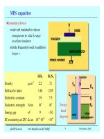
MIS capacitor
•Elementary device
oxide well matched to silicon
transparent to wide range
excellent insulator
nitride frequently used in addition
larger
SiO
2
Si
3
N
4
Density
g.cm
-3
2.2 3.1
Refractive index 1.46 2.05
Dielectric constant 3.9 7.5
Dielectric strength V/cm 10
7
10
7
Energy gap
eV 9 ~5.0
DC resistivity at 25C Ω. cm 10
14
-10
16
~10
14
Energy
band
diagram
30 October, 2001
www.hep.ph.ic.ac.uk/~hallg/
17
MOS capacitor characteristics
•Apply bias voltage to influence charge under oxide
depletion - potential well which can store charge
inversion - thin sheet of charge with high density
allows conduction in transistor
very close to Si-SiO
2
interface
Basis of MOS
transistor operation
Basis of MOS
transistor operation
30 October, 2001
www.hep.ph.ic.ac.uk/~hallg/
18
CCD - Charge Coupled Device
1
2
3
drive pulses
polysilicon electrodes
1µm
signal electrons
in
buried channel
22µm
silicon substrate
gate
insulator
column
isolation
22µm
φ
φ
φ
•2-d array of MOS capacitors
electrode structures isolate pixels
allow to transfer charge
thin sensitive region
signals depend on application
low noise, especially if cooled
•Video requirements different to
scientific imaging
persistent image
smaller area & pixels
Readout time long ms-s
all pixels clocked to readout node
•Applications
astronomy, particle physics, x-ray
detection, digital radiography,
30 October, 2001
www.hep.ph.ic.ac.uk/~hallg/
19
CCD charge transfer
φ
2
φ
1
3
φ
t
1
t
2
t
3
V
G
0V
0V
+V
G
+V
G
0V
0V
+V
G
0V
0V 0V
+V
G
0V
t
1
t
2
t
3
3
1 2 3
•Change voltages on pixels in regular way ("clock")
3 gates per pixel
3 phases per cycle
depletion depth in adjacent regions changes
E field transfers charge to next pixel
- finally to output register
30 October, 2001
www.hep.ph.ic.ac.uk/~hallg/
20
Silicon detector radiation damage
•As with all sensors, prolonged exposure to radiation creates some permanent damage
- two main effects
Surface damage Extra positive charge collects in oxide
all ionising particles generate such damage
MOS devices - eg CCDs - are particularly prone to such damage
Microstrips - signal sharing & increased interstrip capacitance - noise
Bulk damage atomic displacement damages lattice and creates traps in band-gap
only heavy particles (p, n, π, …) cause significant damage
increased leakage currents - increased noise
changes in substrate doping
30 October, 2001
www.hep.ph.ic.ac.uk/~hallg/
1
Signals
•Signal
generalised name for input into instrument system
•Might seem logical to consider signals before sensors but can now see
wide range of signal types are possible
depend on sensor
depend on any further transformation - eg light to electrical
•Most common types of signal
short, random pulses, usually current, amplitude carries information
typical of radiation sensors
trains of pulses, often current, usually binary
typical of communication systems
continuous, usually slowly varying, quantity - eg. current or voltage
slow - typical of monitoring instruments
fast - eg cable TV, radio
•terms like “slow”, “fast” are very relative!
30 October, 2001
www.hep.ph.ic.ac.uk/~hallg/
2
Typical signals
•Some examples
•However, we will find later that speed of signal is not always sufficient to build fast
responding systems
Signal source Duration
Inorganic scintillator e
-t
/τ
τ ~ few µs
Organic scintillator e
-t
/τ
τ ~ few ns
Cerenkov ~ns
Gaseous few ns - µs
Semiconductor ~10ns
Thermistors continuous
Thermocouple continuous
Laser pulse train ~ps rise time
or short pulses ~fs
30 October, 2001
www.hep.ph.ic.ac.uk/~hallg/
3
Signal formation
•Issues in practical applications
duration
radiation: depends on transit time through sensor and details of charge induction
process in external circuit
linearity
most radiation sensors characterised, or chosen for linearity
for commercial components can expect non-linearity, offset and possible
saturation
reproducibility
eg. many signals are temperature dependent in magnitude - mobility of charges
other effects easily possible
ageing
sensor signals can change with time for many reasons
natural degradation of sensor, variation in operating conditions, radiation
damage,
•all these effects mean one should always be checking or calibrating measurements
intended for accuracy as best one can
30 October, 2001
www.hep.ph.ic.ac.uk/~hallg/
4
Optical transmitters
E
g
•Semiconductor lasers most widely used
Now dominate telecomms industry
>> Gb/s operation
•Principle
Forward biased p-n diode
=> population inversion
direct band gap material
GaAs ~850nm
GaAlAs ~ 600-900nm
In, Ga, As, P ~0.55-4µm
•+ polished optical facets
=> Fabry-Perot cavity
optical oscillator
lase at I > I
threshold
photon losses from cavity or absorption
often very linear
8
6
4
2
0
2520151050
Current (mA)
un-irradiated
after 2x10
14
n/cm
2
1nsec
30 October, 2001
www.hep.ph.ic.ac.uk/~hallg/
5
Modern semiconductor lasers
•Quantum well structures
confine charge carriers to active layer
refractive index difference
=> waveguide confines light
minimise lateral dimensions for efficiency
& low I
threshold
=>low power (~mW), miniature devices
well matched for optical fibre transmission
•VCSELs Vertical Cavity Surface Emitting Laser
emit orthogonal to surface
ultra-low power
cheap to make (test on wafer)
can be made in arrays
non-linear L-I characteristic
but very suitable for digital applications
30 October, 2001
www.hep.ph.ic.ac.uk/~hallg/
6
Passage of radiation through matter
•Need to know a few elementary aspects of signal formation whether interested in
light or other radiation
How far does radiation penetrate?
How much of incident energy is absorbed?
•Signal current - duration and magnitude
consequence of charge carriers generated
electrons + holes (semiconductor) or ions (gases, liquids)
current duration depends on
distance over which charge deposited
rapid absorption or thin sensor give fast signals
electric field
only charges in motion generate currents
current in external circuit is induced
30 October, 2001
www.hep.ph.ic.ac.uk/~hallg/
7
Light
•I ~ I
0
exp(-L/L
abs
)
1/L
abs
= N
atom
σ N
atom
= ρN
Avogadro
/A = no. atoms per unit volume
•Photoabsorption
E ~ eV- 100keV atom ionised in single process, all photon energy transferred
at low energies depends on atomic properties of material
at higher energies σ
pa
~ Z
4-5
/E
γ
3
above K-shell edge
•Compton scattering
~MeV quantum collision of photon with charged particle, usually e
-
transfer of part of photon energy, often small
•Pair production
>> MeV
all energy transferred to e+e- pair
to conserve momentum and energy, needs recoil
must take place in field of nucleus or electron
30 October, 2001
www.hep.ph.ic.ac.uk/~hallg/
8
Light absorption-
•Low energies
see consequence of atomic behaviour
eg silicon bandgap
NB strong dependence on wavelength in near-visible regions
•High energies
atomic shell structure
visible
then electrons appear
as quasi-free
Compton scattering
starts to dominate
at ~60keV - not shown
10
-2
10
0
10
2
10
4
10
6
10
8
Absorption length [
µ
m]
0.01 0.1 1 10 100 1000
Photon energy [keV]
Silicon
30 October, 2001
www.hep.ph.ic.ac.uk/~hallg/
9
Light absorption
•Far UV to x-ray energies
atomic shell structure
photo-absorption
coherent = Rayleigh scattering
atom neither ionised nor nor excited
incoherent = Compton
= Zf(E )
pair production E
γ
> 2m
e
contributions from nucleus (~Z
2
)
and atomic electrons (~Z)
small contribution from nuclear interactions
30 October, 2001
www.hep.ph.ic.ac.uk/~hallg/
10
Charged particles
•Ionisation dominates Units: x = density x thickness = [g.cm
-2
]
Stopping power = dE/dx scales in similar way for all particles with p/m = βγ
dominated by interactions with
atomic electrons
•low energies
slow particles lose energy rapidly
dE/dx increases with
to maximum
Bragg peak
•relativistic energies
decline ~ 1/β
2
to minimum value
further slow rise ~ log(p/m)
•most cosmic rays and high energy
particles approximately MIPs
30 October, 2001
www.hep.ph.ic.ac.uk/~hallg/
11
dE/dx
•Measured energy loss can provide another way of identifying particles
gas detectors with multiple samples of ∆E from same particle
momentum measurement is needed - from bending in B field
accompanied by good calibration of p and dE/dx
30 October, 2001
www.hep.ph.ic.ac.uk/~hallg/
12
Electrons
•are special because of their low mass
classically accelerated charge radiates
•brehmstrahlung radiation in matter
acceleration in nuclear field
•synchrotron radiation in accelerators
generates beams of low energy x-rays
typical E ~ 1-10keV
widely used for studying atomic properties, eg protein crystallography
30 October, 2001
www.hep.ph.ic.ac.uk/~hallg/
13
Other neutral particles
•neutrons
do not generate ionisation directly so hard to measure
•at low energies
mostly elastic collisions with atoms in material
simple kinematics determines energy transfer
∆T
max
= 4AT
inc
/(1+A)
2
low Z materials favoured to absorb neutron energy
C, D
2
O moderators in nuclear reactors
hydrogenous or boron compounds used as detectors
30 October, 2001
www.hep.ph.ic.ac.uk/~hallg/
14
Sensor equivalent circuits
•Many of the sensors considered so far can be modelled as
current source + associated capacitance
typical values ~ few pF
but can range from
~100fF semiconductor pixel
~10-20pF gas or Si microstrip, PM anode
~100pF large area diode
~µF wire chamber
usually there is some resistance associated with the sensor, eg leads or
metallisation but this has little effect on signal formation or amplification
•Notable exception: microstrips - gas or silicon
the capacitance is distributed, along with the strip resistance
forms a dissipative transmission line
C
det
i
signal
Z
L