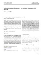
ultrafast two color ablation of fused silica
Bạn đang xem bản rút gọn của tài liệu. Xem và tải ngay bản đầy đủ của tài liệu tại đây (313.67 KB, 4 trang )
DOI: 10.1007/s00339-005-3476-x
Appl. Phys. A 83, 49–52 (2006)
Materials Science & Processing
Applied Physics A
i.h. chowdhury
1
x. xu
1,✉
a.m. weiner
2
Ultrafast two-color ablation of fused silica
1
School of Mechanical Engineering, Purdue University, West Lafayette, IN 47907, USA
2
School of Electrical and Computer Engineering, Purdue University, West Lafayette, IN 47907, USA
Received: 31 August 2005/Accepted: 23 November 2005
Published online: 17 January 2006 • © Springer-Verlag 2005
ABSTRACT Two ultrafast laser pulses at the fundamental
Ti:sapphire laser wavelength of 800 nm and the second har-
monic at 400 nm were used to study the temporal evolution of
the transmissivity in fused silica and resulting material ablation.
It was observed that there was a sharp drop in the transmissivity
of the probe pulse at zero delay between the two pulses, indi-
cating that there was enhanced absorption/reflection due to the
creation of defect states or free electron plasma by the pump
pulse. Subsequent atomic force microscopy measurements of
the ablated holes revealed that the ablated volume increased by
about 50% when the separations of the two pulses are within
300 fs. Two-color machining of channels at the surface also
showed a similar increase in the machined depth and width
when the pulses are overlapped in time.
PACS 52.38.Mf; 78.47.+p; 79.20.Ds
The use of ultrafast laser pulses for machining wide band-gap
dielectrics, materials that are normally transparent to visible
or near-infrared light, has been widely studied in recent years.
The extremely high peak intensities that these amplified ultra-
fast pulses can achieve drive nonlinear absorption processes
due to tunneling, multiphoton, and avalanche ionization. Sev-
eral comprehensive reviews ofthe topic canbe foundin the lit-
erature [1, 2]. Recent studies [3, 4] have revealed the temporal
dynamics of the absorption processes, showingthe creation of
dense free electron plasma and also rapid structural change at
the surface on the order of a few picoseconds.
A related issue is the investigation of the type of defect-
related absorption states that might contribute to enhanced
absorption of the ultrafast laser pulses. To understand these
phenomena better, it is useful to undertake pump-probe stud-
ies at different wavelengths to complement the existing liter-
ature. Also, using higher energy photons can help in exciting
electrons from the valence band to intermediate states which
can easily absorb light from the fundamental wavelength to
cross the band-gap. Such a process has been reported in fused
silica [5]. Two different nanosecond lasers were used in that
✉ Fax: +1-765/494-0539, E-mail:
study – a VUV F
2
laser at 157 nm (7.9eV) and an UV KrF
excimer laser at
248 nm (5eV). A combination of the VUV
and the UV photons are enough to excite an electron to the
conduction band. This two-step process has been shown to be
very efficient and is much more cost-effective than using the
F
2
laser alone for ablation as the output power of this laser is
quite low.
The amplified femtosecond laser has a high enough in-
tensity to photoexcite electrons by multiphoton and tunneling
ionization. However, it would be interesting to see if the use
of both the fundamental
800 nm and the second harmonic
400 nm photons together could lead to enhanced absorption
due to defect related energy states. Some work similar to this
has been reported in the literature. A combination of the fun-
damental and second-harmonic beams of a Ti:sapphire laser
were used to ablate polyethylene (PE) samples [6]. It was
found that usinga small amount of the second-harmonic beam
at
395 nm (2mJ/cm
2
) along with 78 mJ/cm
2
of the funda-
mental at
790 nm led to a 12-fold enhancement in the etch
depth as compared to the case where only the fundamental
beam was used. However, thisstudy did not look at the tempo-
ral dynamics of the modification process and no mention was
made of the temporal separation of the
790 nm and 395 nm
pulses during the course of the experiment. Another similar
study was reported [7] where a combination of
180 fs pulses
centered at
800 nm and 15 ns pulses at 532 nm were used to
ablate fused silica and quartz samples. It was found that when
the nanosecond pulse was delayed by about
30 ns behind the
femtosecond pulse, the ablated volume increased by a factor
of about two. This phenomenon was attributed the creation
of free electrons and defect states by the femtosecond pulse
which could be exploited by the longer pulse.
The experimental setup used in this study has a conven-
tional pump-probe geometry that has been described in detail
in a previous article [4]. In brief,
90 fs FWHM pulses cen-
tered at
800 nm produced by a Spectra-Physics Spitfire re-
generative amplifier are separated by a beamsplitter and sent
along two separate paths. One path has an adjustable delay
while the other one is fixed. A type-I phase-matched BBO
crystal was inserted in the delay arm to generate the second-
harmonic pulse at
400 nm. Both the pulses were focused onto
the sample with a long-working-distance Mitutoyo objective
(
10×, 0.28 NA). The transmitted light after the sample was
50 Applied Physics A – Materials Science & Processing
collected with another objective (50×, 0.5NA). Appropriate
color filters were placed in front of the photo-detector meas-
uring the transmissivity after the collecting objective to detect
either 400 or
800 nm wavelengths, as necessary. All the re-
sults reported here, except the channel machining data, were
collected in single-shot mode to avoid any possible incuba-
tion effects [8]. BBO has an inverse group-velocity mismatch
(GVM) value of
β = 194 fs/mm [9]. Using a sum of squares
approximation, the
400 nm pulses produced in the 0.5mm
thick BBO crystal were estimated to have a longer pulse-
width of about
132 fs. Both pulses are focused to the sample
surface with a diameter of about
4 µm. All experiments were
conducted in air at atmospheric pressure. The samples used
were
1mmthick fused silica (Corning 7980) which were first
cleaned with acetone and methanol.
One concern was the effect of chromatic aberration due to
the fact that the same objective lens was used to focus both
the
800 nm and 400 nm pulses. In order to test this, single-
shot
Z-scan [10] measurements were performed on the sam-
ple. Measurements were taken at both
400 nm and 800 nm
separately with equal energies of about 0.4 µJ/pulse in both
cases. It was found that both wavelengths showed very similar
z-dependence of the transmissivity across the sample surface.
The data are not reproduced here in the interests of brevity.
As such, it can be assumed that the
800 nm and 400 nm pulses
were well-overlapped at the focal position. Next, pump-probe
transmissivity experiments were conducted on the fused sil-
ica sample. Both the
800 nm and the 400 nm pulses were used
as probes alternately and the results are shown in Figs. 1
and 2, respectively. In this study, both the pump and probe
pulses have comparable energies, which is in contrast to the
usual convention wherein the probe is much weaker than the
pump. We define the probe as the pulse whose transmissivity
is measured by the detector. In all the plots, positive delay cor-
responds to the case where the probe comes after the pump
and vice versa for negative delay. The maximum energy in
the
400 nm beam that could be delivered to the sample was
about
0.4 µJ because of constraints in how much 800 nm en-
ergy could be used to pump the BBO crystal and also the loss
due to reflectivity of the mirrors and beamsplitters in the op-
tical path. Much higher energies could be delivered at
800 nm
and this beam was used to carry out the actual ablation while
the
400 nm beam was used to only modify the dynamic ab-
sorption characteristics.
Figure 1 shows time-resolved transmissivity of an
800 nm
probe pulse at 0.47 µJ at three different 400 nm pump energy
levels (in
µJ). Figure 2 shows time-resolved transmissivity
of a
400 nm probe pulse at 0.4 µJ at four different 800 nm
pump energy levels (in µJ). It is seen from Figs. 1 and 2
that both sets of data display a drop in the transmissivity
near zero delay due to the creation of free carriers or de-
fect states by the pump pulse. The feature that distinguishes
the two plots is the fact that there is a rapid (
∼ 1ps) recov-
ery in Fig. 1 but not in Fig. 2. Comparing transmissivity ob-
tained at the same pump energy level of
0.4 µJ (the lowest
level in Fig. 2), we see a complete recovery in transmissiv-
ityforthecaseofthe
400 nm pump but not for the 800 nm
pump. These can be explained in the following terms. The
fast trapping seems to agree with previous reports in the lit-
erature that the free carriers in fused silica are trapped very
FIGURE 1 Time-resolved transmissivity of an 800 nm probe pulse at
0.47 µJ at three different 400 nm pump energy levels (in µJ)
FIGURE 2 Time-resolved transmissivity of a 400 nm probe pulse at 0.4 µJ
at four different 800 nm pump energy levels (in µJ)
rapidly due to the formation of self-trapped excitons (STEs)
with a time constant of about
150 fs [11]. These STEs exhibit
transient absorption bands at
4.2eVand 5.2eVand lumines-
cence bands at
2.5eVand 2.8eV[12]. These are energy levels
that can be accessed more easily by the higher energy
400 nm
photons than by 800 nm photons. Also, previous studies [13]
have identified defect states in fused silica, such as the non-
bridging oxygen hole center (NBOHC) at
2.0eVand the Si
E
center at 5.6eV. It is possible that the 400 nm pump cre-
ates these defect states which are not accessible by the
800 nm
(1.5eV) photons. On the other hand, the defect states cre-
ated by the
800 nm pump might easily absorb the 400 nm
(3.1eV) probe photons, especially if they are at NBOHC-type
levels.
At the higher pump energy levels (
1.0 µJ and above)
shown in Fig. 2, the transmissivity stays at a lower level. This
is due to the fact that at these pump energy levels, there is
permanent surface damage, which reduces the transmissiv-
ity of the probe pulse. This has also been seen in previous
800 nm pump – 800 nm probe experiments [3, 4]. Under the
focusing conditions employed in this experiment, the focal
spot size is about
4 µm which yields a damage threshold for
fused silica of
5.5 ×10
13
W/cm
2
at 800 nm [4]. This corres-
ponds to an energy value of about
0.62 µJ/pulse. Damage
at
400 nm was found to occur at a lower energy level of
about
0.4 µJ/pulse. Note in all the experiments, the transmis-
sion data are normalized with respect to the transmission of
the probe at long negative delay; therefore, the self absorp-
tion effect of the probe pulse is already included in these
data.
CHOWDHURYet al. Ultrafast two-color ablation of fused silica 51
In order to take advantage of the enhanced absorption
that should accompany the decrease in transmissivity seen
in the pump-probe experiments in Fig. 1, two-color ablation
experiments were conducted. The results of ablation volume
together with the transmission data are shown in Fig. 3. The
experiments were done with a single
800 nm pulse at 1.0 µJ
and with a 400 nm pulse at 0.4 µJ placed at varying delay
times before it. In this plot, positive delay corresponds to the
800 nm pulse coming after the 400 nm pulse. The transmis-
sivity of the
800 nm pulse is measured. All the data-points
shown in Fig. 3 are averaged over three experiments. A sin-
gle
800 nm pulse at 1.0 µJ ablates about 0.47 µm
3
of mate-
rial while a single
400 nm pulse at 0.4 µJ ablates a volume
of about
0.02 µm
3
under the focusing conditions employed
in this experiment. The corresponding maximum depths are
305 nm and 38 nm, respectively. When two pulses are used,
the ablation volume varies with the time delay between the
two pulses. There is an increase in the ablation volume at
zero time delay as shown in Fig. 3, which corresponds to the
transmissivity dip at zero delay. Up to delays of about
300 fs,
the ablated volume exceeds the volume ablated by a single
800 nm pulse by about 50%. This enhancement in ablation is
due to the increased absorption of the
800 nm pulse which fol-
lows the
400 nm pulse due to the creation of defect states or
free electron plasma by the
400 nm pulse. However, an ex-
act correlation of
∼50% increases in ablation with the ∼40%
decreases in transmissivity is not possible because of two rea-
sons. Firstly, the ablation rate is not linearly related to the
absorbed energy. Secondly, the drop in transmissivity indi-
cates an increase in absorption but an exact energy balance is
not possible since reflected and scattered light is not measured
in this study.
When the
0.4 µJ case in Fig. 1 is compared with the trans-
missivity data in Fig. 3, it is seen that the latter has a longer-
lived drop. This is attributed to the fact that the
800 nm pulse
FIGURE 3 Time-resolved measurements of transmissivity and ablated vol-
ume for an 800 nm pulse at 1.0 µJ with a 400 nm pre-pulse at 0.4 µJat
different delays (T: transmissivity, V: ablated volume)
FIGURE 4 Optical micrograph of ablated holes in fused
silica (numbers at the bottom indicate delay between 800 nm
and 400 nm pulses in picoseconds)
energy used in Fig. 3 is much higher (1.0 µJ as compared to
0.47 µJ in Fig. 1). As such, nonlinear absorption mechanisms
that occur at higher energy or intensity levels could be en-
abled. The
800 nm (1.5eV) photons can thus be absorbed in
NBOHC (
2eV)orSiE
type defect levels (5.6eV)andalso
in the
4.2eVand 5.2eVabsorption bands of the STEs cre-
ated by the
400 nm pre-pulse, which would not be possible
under linear absorption. The transmissivity recovery also hap-
pens on a much slower time-scale than the ablation enhance-
ment. This is attributed to the fact that ablation is primarily
a surface phenomenon while the transmissivity drop is also
affected by absorption in the bulk of the material. This is
because the ionization front of the free carrier plasma cre-
ated by the ultrafast laser pulse moves rapidly into the bulk
of the sample [14]. As such, the surface effects happen on
a faster time-scale than the bulk effects. A similar result was
seen in
800 nm pump–800 nm probe experiments reported
previously [4] wherein it was observed that time-resolved re-
flectivity measurements (which depend on the surface condi-
tion) showed a much more rapid decay than the transmissivity
data.
Another interesting feature of the experimental data is that
the volume ablated at longer delays is actually slightly less
than that ablated by a single
800 nm pulse. The AFM pictures
show that the
400 nm pulse causes some surface roughening
due to a small amount of ablation (
∼38 nmcrater depth). This
might increase the scattering of the
800 nm pulse and thus re-
duce the energy coupling. It is also noted that the transmission
is not fully recovered, which is due to scattering caused by the
surface roughening.
Further verification of the increase in ablation is shown
in Fig. 4 which shows a microscope picture of the array of
holes machined at different delays. These holes are the same
as the ones whose AFM-measured volume were plotted in
Fig. 3.Again, positive delay implies that the
800 nm pulse fol-
lows the
400 nm one. It is seen that the holes machined at
zero delay are larger than those machined at longer delays
and also those machined with only a single
800 nm pulse at
the same energy. The holes machined at longer delays tend
to be smaller, displaying the same trend as the AFM meas-
urements discussed in the previous paragraph. Also, chan-
nels were machined with the
1kHzoutput of the regenerative
amplifier by scanning the sample at a speed of
20 µ/s.The
channel at the top in Fig. 5a was machined with a combina-
tion of
400 nm pulses at 0.1 µJ and 800 nm pulses at 1.0 µJ
with zero delay between the pulses. The channel at the bot-
tom was machined with only
800 nm pulses at 1.0 µJ.Ma-
chining with only the 400 nm,
0.1 µJ pulses produced no
visible damage under microscope. It is seen from the fig-
ure that the channel at the top is wider than the one at the
52 Applied Physics A – Materials Science & Processing
FIGURE 5 (a) Optical micrograph of channels machined
in fused silica at a scanning speed of 20 µ/s (scale: 1.0 =
10.0 µm). AFM scans of the cross-section of the chan-
nel machined with (b) 800 nm and 400 nm pulses, and
(c) only 800 nm pulses
bottom with nominal widths of about 6 µm and 4 µm,re-
spectively. Also, AFM measurements shown in Fig. 5b and
c reveal that they had maximum depths of about
2.3 µm
and 1.4 µm, respectively. This result corresponds well to the
single-shot data, which also showed an increase in ablated
volume near zero delay between the
800 nm and 400 nm
pulses.
The single-shot pump-probe experiments reported here
show clearly that there is a temporal delay window during
which enhanced absorption of the second pulse is possible.
This is due to creation of free carriers and defect states by the
preceding pulse which enhance energy absorption of the sec-
ond pulse. This enhancement in absorption translates directly
into an increasein the ablated volume when the pulses are sep-
arated within a certain delay time. These results suggest that
using a combination of the fundamental and the second har-
monic beams might allow us to exploit enhanced absorption
effects for higher ablation rates.
ACKNOWLEDGEMENTS Support to this work by the National
Science Foundation (DMI-0300488) is gratefully acknowledged.
REFERENCES
1 C.B. Schaffer, A. Brodeur, E. Mazur, Meas. Sci. Technol. 12, 1784
(2001)
2 S.S.Mao,F.Qu
´
er
´
e, S. Guizard, X. Mao, R.E. Russo, G. Petite, P. Martin,
Appl. Phys. A 79, 1695 (2004)
3 I.H. Chowdhury, X. Xu, A.M. Weiner, Appl. Phys. Lett. 86, 151 110
(2005)
4 I.H. Chowdhury, A.Q. Wu, X. Xu, A.M. Weiner, Appl. Phys. A 81, 1627
(2005)
5 K. Sugioka, K. Obata, M.H. Hong, D.J. Wu, L.L. Wong, Y.F. Lu,
T.C. Chong, K. Midorikawa, Appl. Phys. A 77, 251 (2003)
6 M. Okoshi, N. Inoue, Appl. Phys. A 79, 841 (2004)
7F.Th
´
eberge, S.L. Chin, Appl. Phys. A 80, 1505 (2005)
8 M. Lenzner, J. Krüger, W. Kautek, F. Krausz, Appl. Phys. A 69, 465
(1999)
9 F. Dmitriev, G.G. Gurzadyan, D.N. Nikogosyan, Handbook of Nonlinear
Optical Crystals (Springer, New York 1997)
10 P.B. Chapple, J. Staromlynska, J.A. Hermann, T.J. McKay, J. Nonlinear
Opt. Phys. 6, 251 (1997)
11 F. Qu
´
er
´
e, S. Guizard, P. Martin, G. Petite, O. Gobert, P. Meynadier,
M. Perdrix, Appl. Phys. B 68, 459 (1999)
12 C. Itoh, K. Tanimura, N. Itoh, J. Phys. C: Solid State Phys. 21, 4693
(1988)
13 P.N. Saeta, B.I. Greene, Phys. Rev. Lett. 70, 3588 (1993)
14 B T.V. Vu, O.L. Landen, A. Szoke, Phys. Plasmas 2, 476 (1995)