optical properties of epitaxial bifeo3thin film
Bạn đang xem bản rút gọn của tài liệu. Xem và tải ngay bản đầy đủ của tài liệu tại đây (773.76 KB, 6 trang )
NAN O E X P R E S S Open Access
Optical properties of epitaxial BiFeO
3
thin film
grown on SrRuO
3
-buffered SrTiO
3
substrate
Ji-Ping Xu
1
, Rong-Jun Zhang
1*
, Zhi-Hui Chen
2
, Zi-Yi Wang
1
, Fan Zhang
1
, Xiang Yu
1
, An-Quan Jiang
2
,
Yu-Xiang Zheng
1
, Song-You Wang
1
and Liang-Yao Chen
1
Abstract
The BiFeO
3
(BFO) thin film was deposited by pulsed-laser deposition on SrRuO
3
(SRO)-buffered (111) SrTiO
3
(STO)
substrate. X-ray diffraction pattern reveals a well-grown epitaxial BFO thin film. Atomic force microscopy study
indicates that the BFO film is rather dense with a smooth surface. The ellipsometric spectra of the STO substrate, the
SRO buffer layer, and the BFO thin film were measured, respectively, in the photon energy range 1.55 to 5.40 eV.
Following the dielectric functions of STO and SRO, the ones of BFO described by the Lorentz model are received by
fitting the spectra data to a five-medium optical model consisting of a semi-infinite STO substrate/SRO layer/BFO
film/surface roughness/air ambient structure. The thickness and the optical constants of the BFO film are obtained.
Then a direct bandgap is calculated at 2.68 eV, which is believed to be influenced by near-bandgap transitions.
Compared to BFO films on other substrates, the dependence of the bandgap f or the BFO thin fi lm on in-plan e
compressive strain from epitaxial structure is received. Moreover, the bandgap and the tra nsition revealed by the Lorentz
model also provide a ground for the assessment o f the bandgap for BFO single crystals.
Keywords: BiFeO
3
thin film, Optical properties, Spectroscopic ellipsometry, Lorentz model, Di electric fun ction
PACS codes: 78.67 n, 78.20 e, 07.60.Fs
Background
BiFeO
3
(BFO) has attracted extensive research activities
as an excellent multiferroic material. It simultaneously
exhibits ferroelectricity with Curie temperature (T
C
=
1,103 K) as well as antiferromagnetism with Neel
temperature (T
N
= 643 K), and the properties make BFO
potential for applications in electronic s, data storage,
and spintronics [1,2]. Especially, the BFO thin film is
paid much attention due to its large spontaneous
polarization, which is an order higher than its bulk
counterpart [3], and then the BFO thin film combined
with nanostructures could be a promising candidate in
the above applications [4]. In addition to its structural
and electronic properties , optical properties of BFO
thin films are focused on [5-9]. H owever, in the pub-
lished literatures on optical studies, the BFO thin film is
usually dire ctly deposited on perovskite oxide SrTiO
3
(STO) and DyS cO
3
(DSO) substrate for epitaxial
growth. So far, there is no report on optical properties of
the BFO thin film with an electrode structure in spite of
the fact that the lower electrode is necessary for the study
on electronic and ferroelectric properties of the BFO thin
film as well as for its applications including nonvolatile
memory devices [10]. Since SrRuO
3
(SRO) is often chosen
as the lower electrode for the BFO thin film as well as for
the buffer layer to control its nanoscale domain architec-
ture [11], it is desirable to investigate the optical properties
of the BFO thin film grown on SRO.
Spectroscopic ellipsometry (SE) is a widely used op-
tical characterization method for materials and related
systems at the nanoscale. It is based on the measuring
the change in the polarization state of a linearly polar-
ized light reflected from a sample surface which consists
of Ψ, the amplitude ratio of reflected p-polarized light to
s-polarized light and Δ, the phase shift difference be-
tween the both [12]. The obtained ellipsometry spectra
(Ψ and Δ at measured wavelength range) are fitted to
the optical model for thin fi lm nanostructure, and thus, rich
* Correspondence:
1
Key Laboratory of Micro and Nano Photonic Structures, Ministry of Education,
Shanghai Engineering Research Center of Ultra-Precision Optical Manufacturing,
Department of Optical Science and Engineering, Fudan University, Shanghai
200433, China
Full list of author information is available at the end of the article
© 2014 Xu et al.; licensee Springer. This is an Open Access article distributed under the terms of the Creative Commons
Attribution License ( which permits unrestricted use, distribution, and reproduction
in any medium, provided the original work is properly credited.
Xu et al. Nanoscale Research Letters 2014, 9:188
/>information including surface roughness, film thickness,
and o ptical constants of nanomaterials are r evealed [13,14].
Since SE allows various characterizations of the material,
our group has studied some th in -film nanostructure using
SE methods [15-18].
In this paper, we report the optical properties of epitax-
ial BFO thin film grown on SRO-buffered STO substrate
prepared by pulsed-laser deposition (PLD) and measured
by SE. The dielectric functions of STO, SRO, and BFO are
extracted from the ellipsometric spectra, respectively. And
the optical constants of the BFO thin film are obtained.
The bandgap of 2.68 eV for the BFO thin film is also re-
ceived and is compared to that for BFO thin film depos-
ited on different substrate as well as BFO single crystals.
Methods
The epitaxial BFO thin film was deposited by PLD on
SRO-buffered (111) STO single-crystal substrate. The
SRO buffer layer was directly deposited on the STO sub-
strate by PLD in advance. More details about the depos-
ition process can be taken elsewhere [19]. The crystal
phases in the as-grown BFO thin film were identified by
X-ray diffraction (XRD, Bruker X-ray Diffractometer D8,
Madison, WI, USA). The surface morphologies of the
BFO thin film were investigated by atomic force micros-
copy (AFM, Veeco Instruments Inc., Atomic Force
Microscope System VT-1000, Plainview, NY, USA). Both
XRD and AFM investigation are employed to show
growth quality of the BFO thin film for further optical
measurement and analysis.
SE measurements were taken to investigate the optical
properties of the BFO fi lm. Considering the optical i nvesti-
gation with respect to a substrate/buffer layer/film struc-
ture, we sho uld firstly obtain the optical response of the
STO substrate and SRO buffer layer and then r esearch the
optical properti es of the BFO thin fil m. T he ellipsom etric
spectra (Ψ and Δ) were collected for the STO substrate, the
SRO buffer layer, a nd the BFO film, respectively, at an inci-
dence angle of 75° in the photon energy range of 1.55 to
5.40 e V by a SOPRA GES5E spectroscopic ellipsometer
(Paris, France), as shown in Figure 1. Afterwards, the ellip-
sometric data, w hich are functions of optical c onstants an d
layer or film thickness, w ere fitted to the corresponding op-
tical model depicted in t he inset of F igure 1. By v aryin g the
parameters of the models in the fitting procedure, the root
mean square er ror ( RMSE) is expressed by [17]
RMSE ¼
ffiffiffiffiffiffiffiffiffiffiffiffiffiffiffiffiffiffiffiffiffiffiffiffiffiffiffiffiffiffiffiffiffiffiffiffiffiffiffiffiffiffiffiffiffiffiffiffiffiffiffiffiffiffiffiffiffiffiffiffiffiffiffiffiffiffiffiffiffiffiffiffiffiffiffiffiffiffiffiffiffiffiffiffiffiffi
1
2n−m−1
X
n
i¼1
Ψ
cal
i
−Ψ
exp
i
ÀÁ
2
þ Δ
cal
i
−Δ
exp
i
ÀÁ
2
hi
s
ð1Þ
is minimized. Here, n is the number of data points in
the spectrums, m is the number of variable parameters
in the model, and ‘exp’ and ‘cal’ represent the experi-
mental and the calculated data, respectively.
Results and discussion
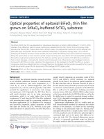
The XRD pattern of the BFO film is displayed in Figure 2
and shows that a strong (111) peak of the BFO matches
the closely spaced (111) ones of the SRO and STO, which
Figure 1 The schematic of SE measurements on BFO thin film with SRO buffer layer structure. (a) STO substrate, (b) SRO buffer layer, and
(c) BFO film. The inset is the optical model of the BFO thin film on the SRO-buffered STO substrate.
Xu et al. Nanoscale Research Letters 2014, 9:188 Page 2 of 6
/>demonstrates a well-heteroepitaxial-grown film that con-
tains a single phase. As given in the inset of Figure 2, the
epitaxial thin film deposited on the SRO/STO substrate is
rather dense with Rq roughness of 0.71 nm. The XRD and
AFM results together reveal a smooth epitaxial BFO thin
film which is beneficial for the optical measurements.
The optical response of the S TO substrate i s calculated
by the pseudo-dielectric function [20], and the obtained di-
electric functions are shown i n Figure 3a, which agrees well
with the published l iterature [ 2 1]. The dielectric funct ions
of SRO were extracted by minimizing the RMSE value
to fit the ellipsometric data of the SRO buffer layer to a
three-medium optical model consisting of a semi-
infinite STO s ubstrate/SRO film/air ambient struc ture.
With the dielec tric functions calculated for the sub-
strate, the free parameters correspond to the SRO-layer
thicknesses and a parameteriz ation of its dielectric func-
tions. The SRO dielectric functions are described in the
Lorentz model expressed by [22].
~
ε ¼ ε
∞
1 þ
X
4
j¼1
A
2
j
E
center
ðÞ
2
j
−EE−iν
j
ÀÁ
!
ð2Þ
The model parameterization consists of four Lorentz
oscillators sharing a high-frequency lattice dielectric con-
stant (ε
∞
). The parameters corresponding to e ach oscil-
lator include oscillator center energy E
center
, oscillator
amplitude A
j
(eV) and broadening parameter ν
j
(eV) .
This model yields thickness 105.15 nm for the SRO
layer and the dielectric spe ctra displayed in Figure 3b.
The c ente r energy of the four oscillators is 0.95, 1.71,
3.18, and 9.89 eV, respectively, and is comparable to the
reported optical transition for SRO at 1.0, 1.7, 3.0, and
10.0 eV [23,24], which indicates that the extracted dielec-
tric functions are reliable.
The inset of Figure 1 sketches a five-medium optical
model consisting of a semi-infinite STO substrate/SRO
layer/BFO film/surface roughness/air ambient structure
employed to investigate the BFO thin film where the
roughness layer is employed to simulate the effect of
surface roughness of the BFO film on SE measurement.
Since the dielectric functions for the STO substrate and
the SRO buffer layer as well as the thickness of SRO
layer have been obtained, the free parameters corres-
pond to the BFO film and surface roughness thicknesses
and a parameterization of the BFO dielectric functions.
The BFO dielectric functions are described by the same
four-oscillator Lorentz model as the SRO layer. And the
surface roughness layer is modeled on a Bruggeman ef-
fective medium approximation mixed by 50% BFO and
50% voids [25]. The fitted ellipsometric spectra (Ψ and Δ)
with RMSE value of 0.26 show a good agreement with the
measured ones, as presented in Figure 4. A BFO film of
99.19 nm and a roughness layer of 0.71 nm are yielded by
fitting the ellipsometric data to the optical response from
the above five-medium model. The roughness layer thick-
ness is exactly consistent with the Rq roughness from the
AFM measurement.
The obtained diele ctric functions of the BFO thin film
are given in Figure 5. In the Lorentz model describing
the dielectric functions, the center energy of four oscilla-
tors are 3.08, 4.05, 4.61, and 5.95 eV, respectively, which
matches well with the 3.09, 4.12, 4.45, and 6.03 eV re-
ported from the first-principles calculation study on
Figure 2 The XRD pattern of BFO thin film deposited on SRO-
buffered STO substrate. The inset shows its AFM image.
Figure 3 The dielectric functions for the STO substrate and SRO buffer layer. (a) STO substrate and (b) SRO buffer layer.
Xu et al. Nanoscale Research Letters 2014, 9:188 Page 3 of 6
/>BFO [26]. The smallest oscillator energy 3.08 eV is ex-
plained either from the occupied O 2p to unoccupied Fe
3d states or the d-d transition between Fe 3d valence
and conduction bands while the other energies can be
attributed to transitions from O 2p valance band to Fe
3dorBi6p high-energy conduction bands [26]. The op-
tical constants refractive index n and extinction coef-
ficient k are calculated through [27]
n ¼ ε
1
þ ε
1
2
þ ε
2
2
ÀÁ
1
2
=
hi
=2
no
1
2
=
ð3Þ
k ¼ −ε
1
þ ε
1
2
þ ε
2
2
ÀÁ
1
2
=
hi
=2
no
1
2
=
ð4Þ
and shown in Figure 6.
Plotting (α▪E)
2
vs E where α is the absorption coeffi-
cient (α =4πk/λ) and E is the photon energy, a linear ex-
trapolation to (α▪E)
2
= 0 at the BFO absorption edge
indicates a direct gap of 2.68 eV according to Tauc's
principle, as shown in Figure 7a. In the plot of (α▪E)
1/2
vs E displayed in Figure 7b, no typical indirect transi-
tions are observed in the spectra range [28], suggesting
that BFO has a direct bandgap. The bandgap 2.68 eV
obtained from the Lorentz model to describe dielectric
functions of the BFO thin film is less than the reported
2.80 eV from the Tauc-Lorentz (TL) model [6]. Since the
TL model only includes interband transitions [29], intra-
band transitions and defect absorption taken account
into the Lorentz model could impact the received band-
gap. In addition, it is reported that there is photolu-
minescence emission peak at 2.65 eV for the BFO film
ascribed to Bi
3+
-related emission [30]. Thus, it is reason-
able to believe that the near-band-edge transition con-
tributes to our shrunk bandgap.
On the other hand, it deserves nothing that there is
controversy about bandgap sensitivity of the epitaxial
thin film to compressive strain from heteroepitaxial
structure [5,7]. Considering that the degree of compres-
sive stress imposed by the epitaxial lower layer progres-
sively decreases with increasing BFO thickness [3], our
result 2.68 eV from the BFO thin film prepared by PLD
with a 99.19-nm thickness is compared to the reported
ones of the BFO film on DSO or STO with comparable
thickness as well as that deposited by PLD, as listed in
Table 1.
Figure 4 The measured and fitted ellipsometric spectra for the BFO film. (a) Ψ and (b) Δ.
Figure 5 The real and imaginary parts of the dielectric function
of the BFO thin film.
Figure 6 Refractive index n and extinction coefficient k of the
BFO film.
Xu et al. Nanoscale Research Letters 2014, 9:188 Page 4 of 6
/>The bandgap of BFO on SRO is almost the same as
that on DSO and is smaller than that on Nb-doped
STO. It is noted that the in-plane (IP) pseudocubic lat-
tice parameter for SRO and DSO is 3.923 and 3.946 Å
[11], respectively, while STO has a cubic lattice param-
eter of 3.905 Å [7]. Considering the IP pseudocubic lat-
tice parameter 3.965 Å for BFO [11], the compressive
strain for the BFO thin film deposited on STO substrate
is larger than that on SRO and DSO. Thus, the more
compressive strain imposed by the heteroepitaxial struc-
ture, the larger bandgap for the BFO thin film, which
agrees with the past report [7].
The obtained direct bandgap 2.68 eV of the epitaxial
BFO thin film is comparable to 2.74 eV reported in BFO
nanocrystals [31] but is larger than the reported 2.5 eV
for BFO single crystals [32]. This can be understood be-
cause even for the epitaxial thin film, the existence of
structural defect such as grain boundaries is evitable,
which will result in an internal electric field and then
widen the bandgap compared to single crystals. On the
other hand, a bandgap of 3 eV for BFO single crystals
through photoluminescence investigation is also re-
ported [33]. The broad and asymmetric emission peak at
3 eV in the photoluminescence spectra presented in [33]
is attributed to the bandgap together with the near-
bandgap transitions arising from oxygen vacancies in
BFO. However, the Lorentz model employed to depict
BFO optical response in our work reveals the existence
of a 3.08-eV transition, which is the transition from the
occupied O 2p to unoccupied Fe 3d states or the d-d
transition between Fe 3d valence and conduction bands
rather than the bandgap [26]. Therefore, the broad and
asymmetric peak is more likely to be explained as the
overlap of the 3.08-eV transition and the bandgap transi-
tion with lower energy.
Conclusions
In summary, the optical properties of the epitaxial (111)
BFO thin film grown on SRO-buffered STO substrate by
PLD were investigated. The XRD and AFM analysis indi-
cated that the BFO thin film sample is grown well with
epitaxial structure and smooth surface. Then SE measure-
ments were taken to get the ellipsometric spectra of the
STO substrate, the SRO buffer layer and the BFO thin
film, respectively, in the photon energy range 1.55 to
5.40 eV. The dielectric functions of STO, SRO, and BFO
are obtained by fitting their spectra data to different
models in which BFO corresponds to a five-medium op-
tical model consisting of a semi-infinite STO substrate/
SRO film/BFO film/surface roughness/air ambient struc-
ture. The BFO film and surface roughness thickness are
identified as 99.19 and 0.71 nm, respectively. The optical
constants of the BFO film are determined through the Lo-
rentz model describing the optical response, and a direct
bandgap at 2.68 eV is obtained which near-bandgap tran-
sitions could contribute to. Moreover, the gap value is
compared to the BFO thin film with similar thickness de-
posited on various substrate prepared by PLD, indicating
the dependence of the bandgap for the epitaxial BFO thin
film on the in-plane compressive strain. In addition, the
transition at 3.08 eV disclosed by the Lorentz model in
our work suggests that the bandgap of BFO single crystals
is less than 3 eV as previously reported. The results given
in this work are helpful in understanding the optical pro-
perties of the BFO thin film and developing its application
in optical field.
Abbreviations
BFO: BiFeO
3
; STO: SrTiO
3
; DSO: DyScO
3
; SRO: SrRuO
3
; SE: spectroscopic
ellipsometry; PLD: pulsed-laser deposition; XRD: X-ray diffraction; AFM: atomic
force microscopy; RMSE: root mean square error; TL: Tauc-Lorentz; IP: in-plane.
Competing interests
We declare that we have no competing interests.
Figure 7 Plot of (α▪E)
n
vs photon energy E. (a) n = 2 and (b) n = 1/2. The plots suggest that the BFO has a direct bandgap of 2.68 eV.
Table 1 Bandgap of BFO thin film (prepared by PLD) on
different substrate
Bandgap (eV) Substrate Film thickness (nm)
2.68 (this work) SRO-buffered STO 99.19
2.67 [8] DSO 100
2.80 [7] Nb-doped STO 106.5
Xu et al. Nanoscale Research Letters 2014, 9:188 Page 5 of 6
/>Authors' contributions
JPX carried out the optical measurements, analyzed the results, and drafted
the manuscript. RJZ proposed the initial work, supervised the sample
analysis, and revised the manuscript. ZHC grew the sample. ZYW and FZ
performed the XRD and AFM measurements. XY helped dealing with the SE
experimental data. AQJ helped the sample growth. YXZ, SYW, and LYC
supervised the sample measurements. All authors read and approved the
final manuscript.
Acknowledgements
This work has been financially supported by the National Natural Science
Foundation of China (Nos. 11174058, 61275160, and 61222407), the No. 2 National
Science and Technology Major Project of China (No. 2011ZX02109-004), and the
STCSM project of China with Grant Nos. 12XD1420600 and 11DZ1121900.
Author details
1
Key Laboratory of Micro and Nano Photonic Structures, Ministry of Education,
Shanghai Engineering Research Center of Ultra-Precision Optical Manufacturing,
Department of Optical Science and Engineering, Fudan University, Shanghai
200433, China.
2
State Key Laboratory of ASIC and System, School of
Microeletronics, Fudan University, Shanghai 200433, China.
Received: 19 February 2014 Accepted: 11 April 2014
Published: 23 April 2014
References
1. Catalan G, Scott JF: Physics and applications of Bismuth Ferrite. Adv Mater
2009, 21:2463–2485.
2. Neaton JB, Ederer C, Waghmare UV, Spaldin NA, Rabe KM: First-principles
study of spontaneous polarization in multiferroic BiFeO
3
. Phys Rev B 2005,
71:014113.
3. Wang J, Neaton JB, Zheng H, Nagarajan V, Ogale SB, Liu B, Viehland D,
Vaithyanathan V, Schlom DG, Waghmare UV, Spaldin NA, Rabe KM, Wutting
M, Ramesh R: Epitaxial BiFeO
3
multiferroic thin film heterostructures.
Science 2003, 299:1719–1722.
4. Martin LW, Crane SP, Chu YH, Holcomb MB, Gajek M, Huijben M, Yang CH,
Balke N, Ramesh R: Multiferroics and magnetoelectrics: thin films and
nanostructures. J Phys Condens Matter 2008, 20:434220.
5. Ihlefeld JF, Podraza NJ, Liu ZK, Rai RC, Xu X, Heeg T, Chen YB, Li J, Collins
RW, Musfeldt JL, Pan XQ, Schubert J, Ramesh R, Schlom DG: Optical band
gap of BiFeO
3
grown by molecular-beam epitaxy. Appl Phys Lett 2008,
92:142908.
6. Kumar A, Rai RC, Podraza NJ, Denev S, Ramirez M, Chu YH, Martin LW,
Ihlefeld J, Heeg T, Schubert J, Schlom DG, Orenstein J, Ramesh R, Collins
RW, Musfeldt JL, Gopalan V: Linear and nonlinear optical properties of
BiFeO
3
. Appl Phys Lett 2008, 92:121915.
7. Himcinschi C, Vrejoiu I, Friedrich M, Ding L, Cobet C, Esser N, Alexe M,
Zahn RT: Optical characterisation of BiFeO
3
epitaxial thin films grown by
pulsed-laser deposition. Phys Status Solidi C 2010, 7:296–299.
8. Basu SR, Martin LW, Chu YH, Gajek M, Ramesh R, Rai RC, Xu X, Musfeldt JL:
Photoconductivity in BiFeO
3
thin films. Appl Phys Lett 2008, 92:091905.
9. Xu XS, Brinzari TV, Lee S, Chu YH, Martin LW, Kumar A, McGill S, Rai RC,
Ramesh R, Gopalan V, Cheong SW, Musfeldt JL: Optical properties and
magnetochromism in multiferroic BiFeO
3
. Phys Rev B 2009, 79:134425.
10. Liu X, Liu Y, Chen W, Li J, Liao L: Ferroelectric memory based on
nanostructures. Nanoscale Res Lett 2012, 7:285.
11. Chu YH, Zhan Q, Martin LW, Cruz MP, Yang PL, Pabst GW, Zavaliche F, Yang SY,
Zhang JX, Chen LQ, Schlom DG, Lin IN, Wu TB, Ramesh R: Nanoscale domain
control in multiferroic BiFeO
3
thin films. Adv Mater 2006, 18:2307–2311.
12. Losurdo M, Bergmair M, Bruno G, Cattelan D, Cobet C, de M artino A,
Fleischer K, Dohcevic-Mitrovic Z, Esser N, Galliet M, G ajic R, Hemzal D,
Hingerl K, Humlic ek J, Ossikovski R, Popovic ZV, Saxl O: Spectroscopic
ellipsometry and polarimetry for materials and systems analysis at the
nanometer scale: state-of-the-art, potential, and perspectives. JNanopart
Res 2009, 11:1521–1554.
13. Xia GQ, Zhang RJ, Chen YL, Zhao HB, Wang SY, Zhou SM, Zheng YX, Yang YM,
Chen LY, Chu JH, Wang ZM: New design of the variable angle infrared
spectroscopic ellipsometer using double Fourier transforms. Rev Sci Instrum
2000, 71:2677–2683.
14. Zhang RJ, Chen YM, Lu WJ, Cai QY, Zheng YX, Chen LY: Influence of
nanocrystal size on dielectric functions of Si nanocrystals embedded in
SiO
2
matrix. Appl Phys Lett 2009, 95:161109.
15. Zhao M, Zhang RJ, Gu HS, Chen MN: Preparation of (Ba
0.5
Sr
0.5
) TiO
3
thin
film by Sol–gel technique and its characteristics. J Infrared Millim Waves
2001, 20:73–76.
16. Zhao M, Zhang RJ, Gu HS, Xu JP: (Ba
0.5
Sr
0.5
) TiO
3
thin film’s preparation
and its electric characteristics. J Infrared Millim Waves 2003, 22:71–74.
17. Chen YM, Zhang RJ, Zheng YX, Mao PH, Lu WJ, Chen LY: Study of the
optical properties of Bi
3.15
Nd
0.85
Ti
3
O
12
ferroelectric thin films. J Korean
Phys Soc 2008, 53:2299–2302.
18. Zhang F, Zhang RJ, Zhang DX, Wang ZY, Xu JP, Zheng YX, Chen LY, Huang RZ,
SunY,ChenX,MengXJ,DaiN:Temperature-dependent optical
properties of titanium oxide thin films studied by spectroscopic
ellipsometry. Appl Phys Express 2 013, 6:121101.
19. Chen ZH, He L, Zhang F, Jiang J, Meng JW, Zhao BY, Jiang AQ: The
conduction mechanism of large on/off ferroelectric diode currents in
epitaxial (111) BiFeO
3
thin film. J Appl Phys 2013, 113:184106.
20. Fujiwara H: Data analysis.InSpectroscopic Ellipsometry: Principles and
Applications. Chichester: Wiley; 2007:147–208.
21. Zollner S, Demkov AA, Liu R, Fejes PL, Gregory RB, Alluri P, Curless JA, Yu Z,
Ramdani J, Droopad R, Tiwald TE, Hilfiker JN, Woollam JA: Optical
properties of bulk and thin-film SrTiO
3
on Si and Pt. J Vac Sci Tehnol B
2000, 18:2242–2254.
22. Shen Y, Zhou P, Sun QQ, Wan L, Li J, Chen LY, Zhang DW, Wang XB:
Optical investigation of reduced graphene oxide by spectroscopic
ellipsometry and the band-gap tuning. Appl Phys Lett 2011, 99:141911.
23. Lee JS, Lee YS, Noh TW, Char K, Park J, Oh SJ, Park JH, Eom CB, Takeda T,
Kanno R: Optical investigation of the electronic structures of Y
2
Ru
2
O
7
,
CaRuO
3
, SrRuO
3
, and Bi
2
Ru
2
O
7
. Phys Rev B 2001, 64: 245107.
24. Wang GT, Zhang MP, Yang ZX, Fang Z: Orbital orderings and optical
conductivity of SrRuO
3
and CaRuO
3
: first-principles studies. J Phys
Condens Matter 2009, 21:265602.
25. Fujiwara H, Koh J, Rovira PI, Collins RW: Assessment of effective-medium
theories in the analysis of nucleation and microscopic surface roughness
evolution for semiconductor thin films. Phys Rev B 2000, 61:10832– 10844.
26. Wang H, Zheng Y, Cai MQ, Huang H, Chan HLW: First-principles study on
the electronic and optical properties of BiFeO
3
. Solid State Commun 2009,
149:641–644.
27. Fujiwara H: Principles of optics. In Spectroscopic Ellipsometry: Principles and
Applications. Chichester: Wiley; 2007:13–48.
28. Basu PK: Interband and impurity absorptions. In Theory of Optical Processes
in Semiconductors. Edited by Kamimura H, Nicholas RJ, Williams RH. Oxford:
Clarendon; 1997:80–122.
29. Jellison GE, Modine FA: Parameterization of the optical functions of
amorphous materials in the interband region. Appl Phys Lett 1996,
69:371–373.
30. Chen X, Zhang H, Wang T, Wang F, Shi W: Optical and photoluminescence
properties of BiFeO
3
thin films grown on ITO-coated glass substrates by
chemical solution deposition. Phys Status Solidi A 2012, 209:1456–1460.
31. Yu X, An X: Enhanced magnetic and optical properties of pure and
(Mn, Sr) doped BiFeO
3
nanocrystals. Solid State Commun 2009, 149:711–714.
32. Palai R, Katiyar RS, Schmid H, Tissot P, Clark SJ, Robertson J, Redfern SAT,
Catalan G: Scott JF: β phase and γ-β metal-insulator transition in multiferroic
BiFeO
3
. Phys Rev B 2008, 77:014110.
33. Moubah R, Schmerber G, Rousseau O, Colson D, Viret M:
Photoluminescence investigation of defects and optical band gap in
multiferroic BiFeO
3
single crystals. Appl Phys Express 2012, 5:035802.
doi:10.1186/1556-276X-9-188
Cite this article as: Xu et al.: Optical properties of epitaxial BiFeO
3
thin
film grown on SrRuO
3
-buffered SrTiO
3
substrate. Nanoscale Research
Letters 2014 9:188.
Xu et al. Nanoscale Research Letters 2014, 9:188 Page 6 of 6
/>