Lcd2 VI XỬ LÝ
Bạn đang xem bản rút gọn của tài liệu. Xem và tải ngay bản đầy đủ của tài liệu tại đây (159.08 KB, 12 trang )
HOW TO USE
INTELLIGENT L.C.D.S
Part Two
By Julyan Ilett
This paper was originally published as the second half of a two-part
article in the March 1997 issue of Everyday Practical Electronics
magazine (www.epemag.wimborne.co.uk), and is reproduced here
with their kind permission.
© Copyright 1997, 1998 Wimborne Publishing Ltd., publishers of
Everyday Practical Electronics Magazine. All rights reserved.
Recreated in Adobe Acrobat PDF format for your web-based reading pleasure by
Maxfield & Montrose Interactive Inc.
www.maxmon.com
How to use
Intelligent L.C.D.s
By Julyan Ilett
An utterly “practical” guide to interfacing
and programming intelligent liquid crystal
display modules.
Part Two
In the first part of this article, the capabilities of character-based liquid crystal display
(l.c.d.) modules were examined, using a few simple, practical experiments. A series of
switches was all that was needed to evaluate the command set in its most fundamental
form, in binary (or hexadecimal).
However, in almost all instances where an l.c.d. is to be used in a design, a microprocessor, or more probably a microcontroller, will be needed to drive it. This is the
subject we examine now.
Good Times
The timing requirements of the HD44780 chip, the controlling device used in most
character-based l.c.d. modules, are illustrated in Figure 6. The diagram provides the
information for both read and write cycles, although some data sheets may show the
two separately. Table 4 details the timing parameters referred to in Figure 6.
RS
RS Valid
tAS
R/W
R/W Valid
tEH
E
tAH
tEL
tRF
tDA
DATA (D0 to D7)
tDS
tDH
Data Valid
Figure 6: HD44780 timing diagram
In the experiments last month, commands were sent to the display by pressing switches on
an experimental test rig. Nothing much went wrong there, so why is it necessary to have
such a complex timing diagram?
Well, we human beings leave plenty of time between pressing one switch and the next, so
the l.c.d. controller can easily keep up with us. Microcontrollers are faster than we are,
though; they can toggle a control line several million times a second, and at such speeds
the l.c.d. controller might not keep pace with the commands.
The timing diagram and its tabulated figures simply tell us how quickly the l.c.d. chip can
respond so that we can program the microcontroller accordingly.
Let's take a typical microcontroller, one of the PIC devices which have become so
popular, and see how we program it to control an l.c.d. from the quoted timing details.
We have published several PIC-based
projects in recent month's which are well
worth studying, along with their software
listings. See the Back Issues and EPE
PCB Service pages. Ed.)
First, though, it must be pointed out that the
discussions from now assume that you have a
rudimentary understanding of programming PIC
microcontrollers, and that you have suitable
software and equipment for doing so. It is not the
intention of this article to teach PIC programming.
The PIC microcontroller would be programmed to start by first setting the l.c.d.'s RS line
to its correct logic level. This is the line that determines whether the l.c.d. should regard
data as control instructions or character information. In cases where data needs to be read
back from the l.c.d., the microcontroller must also have control over the R/W line
(read/write), otherwise it should be connected to ground, as on the test rig.
The microcontroller can set up
these two signals at the same time,
or it may do one before the other, it
doesn't really matter. What is
important, is that they are both
“valid” or “stable” for a minimum
period of time before the level on
the “E” (Enable) line is raised to a
logic 1. On the diagram in Figure 6,
this period is shown as “tAS” (time
– address setup), and in the table
this is specified as 140ns minimum.
It can be more than 140ns, but it
must not be any less.
Table 4: HD44780 Timing Parameters.
Once line E is high, it must not be brought low again until at least 450ns has elapsed, as is
indicated by the “tEH'” (time -- enable high). Also, all eight data lines must be set to their
appropriate logic levels and allowed to stabilise for at least the “tDS” (time -- data setup)
period of 200ns before bringing line E low again.
Note that the l.c.d. allows the data lines to be set up after line E is taken high. In the
experiments last month, data was established well before the E switch was pressed, but
either condition is allowed.
When line E is returned to a low level, there are also two hold times that must be taken
into account. The “tAH” (time -- address hold) parameter indicates that the RS and R/W
lines must not be altered for at least 10ns, and “tDH'” (time -- data hold) shows that none
of the data lines must change for at least 20ns.
One further restriction exists. The E line must not be taken high again (for the next
command, that is) for another 500ns (“tEL”: time -- enable low). This means that the total
cycle time of the E line is 450ns plus 500ns. Allowing for the rise and fall times, indicated
by “tRF”, which should be no longer than 25ns each, an approximate value of 1µs can be
calculated. This means that no more than one million commands (or one million characters)
per second should be sent to the display, not a restriction that would normally present
many problems!
Busy
The timing diagram doesn't tell the whole story, however. Much longer delays are
required to enable the l.c.d. to process commands and data. Most commands tie-up
the l.c.d. for 40µs, during which time it is said to be “busy.” The Clear Display and
Cursor Home commands, though, can
take a lot longer.
Execution times for all the instructions are
shown in Table 5. This includes all the
commands, writing data to the display,
and reading both data and status. The
two Read instructions have not yet been
experimented with, but reading the status
of the l.c.d. is the method used to determine
whether or not it is busy.
The practical implication of these
instruction times is just a case of having to
insert a delay between one instruction and
the next. The first two commands, Clear
Display and Cursor Home, have variable
execution times that depend upon several
factors. Not much is said about this variation in the data sheets, but it does involve
returning the cursor to address 10000000 ($80), unshifting the display and, in the case of
Clear Display, putting a space character into each display address.
There is one other important situation when the l.c.d. will be busy. This is immediately
after it has been powered up. It takes some 10 to 15 milliseconds for the full initialisation
sequence to be completed, during which time no instructions can be executed.
This has important implications for a circuit using a microcontroller. A suitable delay
must be added to the beginning of the program, otherwise the l.c.d. won't be ready when
the first few instructions are sent to it and could become locked up in a non-correctable
condition, requiring the power to be switched off again for a while.
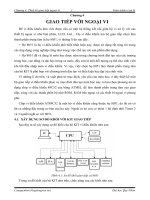
New Circuit
Time now to re-wire last month's experimental test rig to incorporate the PIC microcontroller. The circuit diagram of the modified arrangement is shown in Figure 7. There's
no longer any need for the debounce circuit, the microcontroller provides very clean
output signals. It is not essential to use the PIC16C84 type specified in the diagram, the
54, 56, 61 and 71 types can all be used, but some minor changes may need to be made to
one or two of the pin connections.
However, it is best to experiment with the PIC16C84 since it is the EEPROM (Electrically
Erasable Programmable Read Only Memory) version of the microcontroller.
The use of this version is desirable because several different versions of software will
need to be programmed and erased during the course of experimentation. Other versions
of the microcontroller cannot be erased so easily, indeed some cannot be erased at all
(those referred to as OTP, One-Time Programmable devices, for example).
X1 LCD Module
D7
14
D6
13
D5
12
D4
11
D3
10
D2
9
D1
8
D0
E
7
6
R/W
5
RS
4
Vee
Vdd
Vss
3
2
1
+5V
13
RB7
12
RB6
Vss
(GND) OSC1
5
16
11
RB5
10
RB4
9
8
7
6
RB3
RB2
RB1
RB0
IC1 PIC16C84
OSC2
MCLR
15
4
R1 4k7
C1
47p
RTCC
RA3
RA2
3
2
1
RA1
18
14
Vdd
(V+)
VR1
5k
RA0
17
CW
0V
Figure 7: Circuit diagram for interfacing a PIC16C84
microcontroller to an l.c.d. module.
The microcontroller's Clock Option can be set for RC (resistor/capacitor) or any one of
the XT (crystal) options, but the RC option is cheaper, and precise timing accuracy is not
important in this instance. The values of the resistor R1 and capacitor C1 connected to the
OSC1 input in Figure 7 will give a clock frequency of very approximately 2MHz. For
the time-being, lower values of resistance or capacitance (for faster speeds) should be
avoided, to ensure the software delays are sufficiently long.
The prototype test rig showing the microcontroller in position
(it’s actually a PIC16C54, although a PIC16C84 is recommended).
Experiment 8: PIC Program
Compile and program the contents of Listing 1 into the PIC microcontroller. It has been
written for use with MPALC assembler software, although it can be readily translated to
suit MPASM or TASM assembly.
Listing 1
list
initialize
setports
p=16C84
clrf
clrf
clrf
clrf
clrf
movlw
tris
movlw
tris
shortdelay
0D
0E
0F
05
06
0F8
05
00
06
;tells assembler to generate code for this device
;clear register 0D, counter register
;clear register 0E, short delay register
;clear register 0F, long delay register
;Port A (register 05) outputs all set to logic 0
;Port B (register 06) outputs all set to logic 0
;Port A bits 0, 1, 2 as outputs (E, RS, R/W)
;Port B all bits as outputs (D0 to D7)
(…continued…)
Listing 1 (continued)
longdelay call
shortdelay
decfsz
0F,f
goto
longdelay
functionset bcf
05,02
bcf
05,01
movlw
38
movwf
06
call
pulse_e
call
shortdelay
displayon bcf
05,02
bcf
05,01
movlw
0F
movwf
06
call
pulse_e
call
shortdelay
clrf
0D
message
movf
0D,w
call
text
bsf
05,02
bcf
05,01
movwf
06
call
pulse_e
call
shortdelay
incf
0D,w
xorlw
05
btfsc
03,02
goto
stop
incf
0D,f
goto
message
stop
goto
stop
;Subroutines and text table
shortdelay decfsz
0E,f
goto
shortdelay
retlw
0
pulse_e
bsf
05,00
nop
bcf
05,00
retlw
0
text
addwf
02,f
retlw
‘H’
retlw
‘E’
retlw
‘L’
retlw
‘L’
retlw
‘O’
end
;long delay while lcd initialises
;RS line to 0 (Port A, bit 2)
;R/W line to 0 (Port A, bit 1)
;Function Set command
;put it on the data lines (Port B)
;pulse the E line high (Port A, bit 0)
;RS line to 0 (Port A, bit 2)
;R/W line to 0 (Port A, bit 1)
;Display On/Off & Cursor command
;put it on the data lines (Port B)
;pulse the E line high (Port A, bit 0)
;set counter register to zero
;put counter value in W
;get a character from the text table
;set RS line to 1 (Port A, bit 2)
;set R/W line to 0 (Port A, bit 1)
;put character on the data lines (Port B)
;pulse the E line high (Port A, bit 0)
;delay while l.c.d. is busy
;try incrementing the counter register
;would that make it increase to 5?
;set the zero flag in the status register
;stop if all characters displayed
;increment the counter register
;go back and do the next character
;stop the program running
;delay while l.c.d. is busy
;take E line high
;hold it high for one clock cycle
;take E line low again
;table of characters for message
Once the PIC has been programmed, re-power up the circuit. The word HELLO will
appear on the display. There may seem to be a lot of source code required to do such a
simple job, but the program performs all the setting up that the display needs, and can
form the basis of a more complex system.
Precisely what all these instructions do is important and will be described in some detail.
The first routine, “initialise,” comprises five Clear File (clrf) instructions which set the
contents of five registers to zero. Two of these registers, 05 and 06, relate to output
Ports A and B.
When the microcontroller is powered up, all port pins are automatically set up as inputs, so
that no damage is done to external circuitry. The “setports” routine uses “tris” instructions
to redefine each bit of Ports A and B as either an input or an output.
(Be aware that Microchip, manufacturers of the PIC family, now discourage the use
of “TRIS,” a command becoming incompatable with their newer devices. There are
alternative ways of achieving the same result, as discussed in the PIC data books. Ed.)
The “longdelay” routine keeps the microcontroller occupied while the l.c.d. is initialising.
This delay must be no less than 15ms, but can be more, of course. The routines “functionset”
and “displayon” are very similar and issue hexadecimal commands $38 and $0F (00111000
and 00001111) to the l.c.d. These numbers should be familiar from the experiments carried
out in Part 1.
Both routines contain “call” instructions to two subroutines, “pulse_e” and “shortdelay,”
which can be seen towards the end of the listing. The “message” routine incorporates a
program loop which is executed five times to output the five characters in the text table
(“text”) to the l.c.d. The PIC uses an unusual type of subroutine, comprising a list of
“retlw” (return with literal) instructions which can be used to form tables of data.
Register $0D is used as a counter which is initially set to zero by the “clrf” instruction in
the “initialise” routine. This value is then used as a pointer to the text table which contains
the ASCII characters which spell HELLO.
The “stop” routine locks up the microcontroller to stop it doing anything else. Finally, the
“end” directive is not a program command, but an instruction to tell the assembler to stop
assembling.
A Good Read
The program in Listing 1 only writes to the display. In many applications this is quite
satisfactory, and it has the advantage of allowing the R/W line on the l.c.d. to be connected
to ground, which in turn saves an I/O (input/output) pin on the microcontroller.
It is possible (and sometimes necessary) to read data and status information from the l.c.d.,
but of course the R/W line must be actively connected in order to do this. Reading the
display differs from writing to it in some fundamental ways, so a re-examination of the
timing diagram is now required, as the sequence of events is described.
Lines RS and R/W must be set up first, with R/W being set to a logic 1 this time. If RS is
set high, data is returned indicating the character that is at the current cursor address. If RS
is set low, a status byte is sent back, containing two separate items, bits 0 to 6 holding the
current cursor address, and bit 7 containing the Busy flag.
The two Read instruction formats are shown in Table 6. After the necessary “address setup
time” (tAS), the E line can be taken high. This is the point at which the read cycle differs
from the write cycle, as the l.c.d.'s data lines will switch over to being outputs.
Instruction
RS
Binary
D7
D6
D5
D4
D3
D2
D1
D0
Read Data
High
D
D
D
D
D
D
D
D
Read Status
Low
BF
A
A
A
A
A
A
A
D:
Character data at current cursor address
A:
Current cursor address ($00 to $7f)
BF:
Busy Flag (0 = Ready, 1 = Busy)
Table 6: HD44780 Read Instructions.
Clearly, before the microcontroller starts this read cycle, it must change its data lines
to inputs, otherwise outputs would be connected to outputs and a fight (known as bus
contention) would ensue. In any case, if the microcontroller's data lines were not inputs
at this time, it would not be able to read the data.
It takes a while for the l.c.d. to change its data lines to outputs, and stabilise the data on
them, but it guarantees to do this within 320ns, the “data access time” (tDA). The microcontroller can then read this data in through its inputs, and as soon as it's happy that it's
got it, the E line can go back down.
Most of the information that can be read back from the display must have been written
there by the microcontroller in the first place, which explains why many designs can get
away without having the R/W line connected up.
The Busy flag, though, can be useful to the microcontroller, to avoid using all those delay
routines. For applications which need to put a lot of information on the display in a very
short time, checking the Busy flag is the most efficient way of knowing when the display
is ready.
Experiment 9: Status Reading
In this experiment, the program in Listing 1 will be altered to incorporate checking of
the Busy flag. The plan here is to replace the subroutine “shortdelay,” which has a fixed
delay time, with another routine which will constantly check the Busy flag until it isn't
busy any more.
Listing 2 shows the new subroutine, called “busywait.” All occurrences of the “call
shortdelay” instruction in Listing 1 should be replaced by “call busywait,” including the
three line section headed “longdelay.” The program will put the message onto the display
much more quickly than before, as unnecessary delays are eliminated.
Listing 2
busywait
busyread
movlw
tris
bcf
bsf
nop
bsf
nop
rlf
bcf
nop
nop
btfsc
goto
movlw
tris
retlw
0FF
06
05,02
05,01
0500
06,w
05,00
03,00
busyread
00
06
0
;Port Ball inputs (D0 to D7)
;RS line to 0 (Port A, bit 2)
;R/W line to 1 (Port A, bit 1)
;wait for tAS
;raise E line (Port A, bit 0)
;wait for tDA
;rotate BF into Carry flag
;lower E line (Port A, bit 0)
;wait for tEL
;wait for tEL
;test Carry flag
;if busy, go round again
;PortB all outputs (D0 to D7)
;return to main program
The first two lines of “busywait” change the assignment of Port B, so that all of its I/O
lines become inputs. Following this, the RS and R/W lines are set up ready for the status
read. For short delays, the “nop” (no operation) instruction can be used, it is ideal for the
small delay times required by the l.c.d. interface.
The E line is then sent high and, after a short delay to allow for the data access time (tDA),
the state of the Busy flag is read into the microcontroller. A “rotate left” (rlf) instruction is
used here, to transfer the Busy flag on data line D7, into the PIC's Carry flag, where it can
be stored prior to testing.
Line E is then taken low, after which a test is performed on the Carry flag using the “btfss”
instruction. If the Carry flag is set, then the l.c.d. was busy at the moment the reading was
taken, and the program branches back to perform another status read.
If the l.c.d. is found to be no longer busy, Port B is switched back for all bits to be outputs
and the subroutine returns to the main program. The program uses more code, but saves
time by avoiding unnecessary delays.
Experiment 10: Nibble Mode
The final experiment is to implement 4-bit data transfer mode between the l.c.d. and the
microcontroller. This was examined in Experiment 7 in Part 1, so the technique should
be reasonably well understood.
However, several changes need to be made, both to the circuit and to the program,
details of which will be left to you to fully implement, but the principles involved
are as follows:
Listing 3 shows some of the changes. Data lines D0 to D3 on the l.c.d. should be
disconnected from the microcontroller (see Part 1 for how to deal with these unused
l.c.d. lines). Data lines D0 to D3 on the microcontroller are now free to be used for
other purposes, but for the time being can be left open circuit.
Listing 3
functionset bcf
05,02
;RS line to 0 (Port A, bit 2)
bcf
05,01
;R/W line to 0 (Port A, bit 1)
movlw
20
;1st Function Set command
movwf
06
;put it on the data lines (Port B)
call
pulse_e
;pulse the E line high (Port A, bit 0)
call
busywait
functionset2 bcf
05,02
;RS line to 0 (Port A, bit 2)
bcf
05,01
;R/W line to 0 (Port A, bit 1)
movlw
28
;2nd Function Set command
movwf
0C
;store command temporarily in 0C
call
portnibble
call
pulse_e
;pulse the E line high (Port A, bit 0)
swapf
0C,w
;swap nibbles of 0C, put result in W
call
portnibble
call
pulse_e
;pulse the E line high (Port A, bit 0)
call
busywait
;Additional subroutine for nibble mode
portnibble andlw
0F0
;clear lower 4 bits of W
iorwf
06,f
;OR this with Port B
iorlw
0F
;set lower 4 bits of W
andwf
06,f
;AND this with Port B
retlw
0
As we saw in Part 1, two separate Function Set commands are needed to set up the l.c.d.
First, binary code 00100000 (hexadecimal $20) is sent while the l.c.d. is still in 8-bit
mode, the mode which it automatically adopts when first switched on. This first code is
followed by 00101000 ($28) sent as two separate nibbles, i.e. 0010 and 1000, both sent
on lines D4 to D7. (Don't forget that lines RS and E must be dealt with appropriately
when sending data.)
In Listing 3, the “functionset” routine of Listing 1 has been modified to send $20 instead
of $38, and then a new routine, “functionset2,” has been added, between “functionset” and
“displayon,” to send $2, and then $8. In the new routine, splitting a command byte into
two nibbles is achieved by using the PIC's “swapf” instruction, which exchanges the upper
and lower halves of any register.
The purpose of using 4-bit mode is that the other four bits of Port B (bits 0 to 3) can be
used for something else, so writing data out on the upper half of Port B, must be done in
such a way that it does not affect the lower half. In practice, any of the microcontroller's
data lines can be used to send control the l.c.d., programming the software accordingly.
Individual “bit set” (bsf) or “bit clear” (bcf) instructions could be used to alter each bit in
turn, but there is a simpler, more logical way, literally! A sequence of AND and OR
instructions can be used to handle all eight bits of Port B, masking out those which must
not be changed.
Listing 3 also shows a subroutine called “portnibble” which contains a sequence of four
instructions that do the job. The upper four bits of the W register are transferred to the
upper four bits of Port B, without affecting the lower four bits. A separate “pulse_e” call
must be made for each of the two nibbles transferred, after which a single “busywait”
call is added.
The “portnibble” routine is added to Listing 1 between the end of the “text” table and the
“end” statement.
It is also necessary to alter the “displayon” routine of Listing 1 to operate in 4-bit mode,
in the same way as is done in the “functionset2” routine. You can do the conversion for
yourself to prove that you have understood so far!
More challenging, perhaps, are the modifications that have to be made to the “message”
routine of the program. The procedure is the same, however, two 4-bit transfers being
required instead of one 8-bit transfer. The use of 4-bit data transfer mode does add to the
complexity of the software, but is well worth the effort as four extra I/O pins are released.
Digital Alternatives
So many electronic devices, these days, have a small keyboard and a liquid crystal
display. For example, many of the better portable radio systems have dispensed with the
potentiometer as a volume control, and the variable capacitor as a tuning control, and
opted for a digital data entry and display alternative.
The advantages that such digital systems offer are undeniable, and even for the amateur
constructor are readily achievable using low-cost but powerful microcontrollers, and
inexpensive but versatile displays and keyboards, as the experiments in this two-part
series have hopefully suggested to you.
(We have more PIC-controlled l.c.d. orientated projects in the pipeline. Ed.)