Sustainable Energy Harvesting Technologies Past Present and Future Part 14 pdf
Bạn đang xem bản rút gọn của tài liệu. Xem và tải ngay bản đầy đủ của tài liệu tại đây (499.59 KB, 8 trang )
Design Issues in Radio Frequency Energy Harvesting System
249
Published works have demonstrated the need for a DC-to-DC boost converter placed
between the rectifying antenna circuit (rectenna) and the storage device. Recent efforts
have demonstrated that a 40mV rectenna output DC voltage could be boosted to 4.1 V to
trickle charge some battery. A Coilcraft transformer with turns ratio (N
s
: N
p
) equal to 100
was used in the boost converter circuit. An IC chip leading manufacturer (Linear
Technology Corp., LT Journal, 2010) has released a linear DC-to-DC boost regulator IC
chip capable of boosting an input DC voltage as low as 20 mV and supplying a number of
possible outputs, specifically suited for energy harvesting applications. While this IC is a
great milestone, readers and researchers need to understand the techniques to achieve
such ICs and also the limitations that apply. In the following sub section, we will describe
the methods toward designing a DC-DC boost converter, suitable for micropower RF
energy harvesting.
In the design, we will attempt to clarify the parameters that affect the DC-DC conversion
efficiency. For this design, Envelope simulation in Agilents’s ADS is used. This simulation
technique is the most efficient for the integrated rectenna and DC-DC boost converter
circuits.
1.6.1 DC-DC boost converter design theory and operation
The DC-DC boost converter design theory and actual implementation are presented in this
section. The inequality V
in
≪V
out
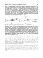
defines the boost operation. In this Chapter, our boost
converter concept is illustrated in Fig. 20. A small voltage, V
in
is presented at the input of the
boost converter inductive pump which as a result, generates some output voltage, V
out
. The
output voltage is feedback to provide power for the oscillator. The oscillator generates a
square wave, F
OSC
that is used for gate signalling at the N-MOSFET switch.
Fig. 20. Boost converter concept.
The drain signal of the N-MOSFET is used as the switch node voltage, V
sn
at the anode of
the diode inside the boost converter circuit block. From the concept presented in Fig. 20, the
actual implemented circuit is shown in Fig. 21. The circuit was designed in Agilent’s ADS
and fabricated for investigation by measurement.
The circuit in Fig. 21 is proposed for investigation. Since a DC-DC boost converter is
supposed to connect to the rectenna’s output, it therefore, becomes the load to the rectenna
circuit. This condition demands that the input impedance of the boost converter circuit
emulates the known optimum load of the rectenna circuit. This has the benefit of ensuring
Sustainable Energy Harvesting Technologies – Past, Present and Future
250
maximum power transfer and hence higher overall conversion efficiency from the rectenna
input (RF power) to the boost converter output (DC power). In this investigation, as shown
in [7], the optimum load for the rectenna is around 2kΩ. In general, emulation resistance R
em
is given by
Fig. 21. The proposed boost converter circuit diagram. Designed in Agilent’s ADS and
fabricated for investigation by measurement.
2
1
21
em
LT M
R
M
tk
(7)
where
L is the inductance equal to 330H as shown in Fig. 20,
out
in
V
M
V
,
T is the period of
F
OSC
, t
1
is the switch”ON” time for the N-MOSFET, and k is a constant that according to [3]
is a low frequency pulse duty cycle if the boost converter is run in a pulsed mode and
typically,
k may assume values like 0.06 or 0.0483. With reference to (7), we select L as the
key parameter for higher conversion efficiency while V
in
= 0.4 V DC is selected as the lowest
start up voltage to achieve oscillations and boost operation. Computing the DC-DC boost
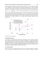
conversion efficiency against different values of L, we have results as shown in Fig. 22.
From the results above, L = 100H is the optimum boost inductance that ensures at least
16.5% DC-DC conversion efficiency, given R
L
= 5.6kΩ.
Now having selected the optimum boost inductance given some load resistance, the
emulation resistance shown in Fig. 23 is evaluated from the ratio of voltage versus current at
the boost converter circuit’s input.
The results show a constant resistance value against varying inductance. In general, we can
say that this boost converter circuit has a constant low input impedance around 82.5Ω. This
impedance is too small to match with the optimum rectenna load at 2kΩ. This directly
affects the overall RF-to-DC conversion efficiency.
Design Issues in Radio Frequency Energy Harvesting System
251
The results show a constant resistance value against varying inductance. In general, we can
say that this boost converter circuit has a constant low input impedance around 82.5Ω. This
impedance is too small to match with the optimum rectenna load at 2kΩ. This directly
affects the overall RF-to-DC conversion efficiency.
DC-DC Efficiency [p.c]
Boost Inductance, L [uH]
0
50 100 150 200 250 300 350
20
40
60
80
100
Fig. 22. Boost inductance variation with DC-DC conversion efficiency for a 5.6 k load.
Emulation Resistance [Ohms]
Booster Inductance, L [uH]
0 50 100 150 200 250 300 350
70
75
80
85
90
Fig. 23. Boost converter’s input impedance: the emulation resistance.
Another factor, which affects the overall conversion efficiency is the power lost in the
oscillator circuit. Unlike the circuit proposed in [9], which uses two oscillators; a low
frequency (LF) and high frequency (HF) oscillator; in Fig. 21, we have attempted to use a
single oscillator based on the LTC1540 comparator, externally biased as an astable
multivibrator.
The power loss in this oscillator is the difference in the DC power measured at Pin 7
(supply) to the power measured at pin 8 (output). We term this loss, L
osc
; converted to heat
or sinks through the 10MΩ load. A comparison of the oscillator power loss to the power
available at the boost converter output is shown in Fig. 24.
Looking at Fig. 24; we notice that the power loss depends on whether the oscillator output is
high or low. The low loss corresponds to the quiescent period where the power lost is
Sustainable Energy Harvesting Technologies – Past, Present and Future
252
almost negligible. However, during the active state, the lost power (power consumed by the
oscillator) nearly approaches the DC power available at the boost converter output. This
results in low operational efficiency.
DC Power [mW]
Time [msec]
Booster output power
Oscillator power loss
Quiescent loss
11.21.41.61.82
0
0.1
0.2
0.3
0.4
Fig. 24. The power loss in the oscillator.
To confirm whether or not the circuit of Fig. 21 works well, we did some measurements and
compared them with the calculated results. Unlike in calculation (simulation), during
measurement, L = 330H was used due to availability. All the other component values
remain the same both in calculation and measurement. In Fig. 25 (left side graph) and (right
side graph), we see in general that the input voltage is boosted and also that the patterns of
F
osc
and V
sn
are comparable both by simulation and measurement. To control the duty cycle
of the oscillator output (F
osc
), and the level of ripples in the boost converter output voltage
(V
out
), we change the value of the timing capacitance, C
tmr
in the circuit of Fig. 21.
Simulations in Fig. 25 (left side graph) show that C
tmr
= 520pF realizes a better performance
i.e. nearly constant V
out
level (very low ripple).
Voltage [V]
Time [msec]
Vin (Low input voltage)
Fosc, Ctmr = 520 pF
Fosc, Ctmr = 820 pF
Vsn, Ctmr = 520 pF
Vsn, Ctmr = 820 pF
Vout, Ctmr = 520 pF
Vout, Ctmr = 820 pF
11.21.41.61.82
-0.5
0
0.5
1
1.5
2
2.5
3
3.5
4
4.5
5
5.5
6
Fosc (Gate Signal)
Vsn (Switching signal)
Vout (Boosted voltage)
Vin (Low input voltage)
Voltage [V]
Time [microsec]
-200 -100 0
100 200
-1
0
1
2
3
4
5
6
7
8
Fig. 25. Voltage characteristics of the developed boost converter circuit. The left side graph
represents simulation while the right side graph is for measurements.
Generally, we observe that with this kind of boost converter circuit topology, it is difficult to
start up for voltages as low as 61.7mV DC generated by the rectenna at -20dBm power
Design Issues in Radio Frequency Energy Harvesting System
253
incidence and at least 18.2% rectenna RF-to-DC conversion efficiency. Self starting is the
issue for this topology at very low voltages.
At least 11.3% DC-DC conversion efficiency was recorded by measurement and is
comparable to the calculation in Fig. 22. During measurement it was clearly revealed that
the boost converter efficiency does depend on the value of
L and the duty cycle derived
from
t
1
. To efficiently simulate the complete circuit, from the RF input to the DC output,
envelope transient simulation (ENV) in Agilent’s ADS was used. The (ENV) tool is much
more computationally efficient than transient simulation (Tran). This simulation is
appropriate for the boost converter circuit’s resistor emulation task. Moreover, the boost
converter’s DC-DC conversion efficiency, and the overall RF-to-DC conversion efficiency
can be calculated at once with a single envelope transient simulation.
In summary, though not capable to operate for voltages as low as 61.7mV DC, the proposed
boost converter has by simulation and measurement demonstrated the capability to boost
voltages as low as 400mV DC, sufficient for battery or capacitor recharging, assuming that
the battery or the capacitor has some initial charge or energy enough to provide start-up to
the boost converter circuit.
The limitations of our proposed boost converter circuit include; low efficiency, lack of self
starting at ultra low input voltages, and unregulated output. To address these limitations,
circuit optimization is required. Moreover, alternative approaches which employ a flyback
transformer to replace the boost converter inductance must be investigated. A regulator
circuit with Low Drop Out (LDO) is necessary to fix the boost converter output voltage
commensurate with standard values like 2.2 V DC for example. For further reading, see [7]
2. Performance analysis of the complete RF energy harvesting sensor
system
To demonstrate how one may analyze the performance of an RF energy harvesting system
including its application, we extend the discussion of Section 2.5.2 to this Section. We propose
a transmitter assembled as in Fig. 26 for temperature sensor wireless data transmission.
Fig. 26. The assembly and test platform for the proposed battery-free sensor transmitter.
Sustainable Energy Harvesting Technologies – Past, Present and Future
254
The transmitter consists of one-chip microcomputer (MCU) PIC16F877A and wireless
module nRF24L01P for the control, and MCU can be connected with an outside personal
computer using ICD-U40 or RS232 cable. The wireless module operates in transmission and
reception mode, and controls power supply on-off, transmitting power level, the receiving
mode status, and transmission data rate via Serial Peripheral Interface (SPI). Figure 27
shows the operation flow when transmitting.
Fig. 27. Operation flow during transmission.
The experimental system composition is shown in Fig. 28 to transmit acquired data by the
temperature sensor with WLAN at 2.4 GHz (ISM band). An ISM band sleeve antenna is
used for the transmission. Using the cellular band rectenna shown and discussed in Section
2.5.1, at least 3.14 V is stored in the electric double layer capacitor over a period of four
hours. To harvest a maximum usable power for the overall system, we charge the capacitor
up to 5V. The operation voltage for the wireless module presented in Fig. 26 above is
between 1.9V and 3.6V.
The signal was transmitted from the wireless module while a sleeve antenna, same like the
one for transmission was used with the spectrum analyzer and the reception experiment
was performed. Received signal level equal to -43.4dBm was obtained at a distance 3.5m
between transmitter and reception point. The capacitor’s stored voltage was used to supply
the wireless module in the above-mentioned experiment. Successful transmission was
possible for 5.5 minutes after which, the capacitor terminal voltage decreased from 3.16V to
1.47V, and the transmission ended. The sending and receiving distance of data can be
estimated to be about 10m when the sensitivity of the receiver is assumed to be -60dBm,
given 0dBm maximum transmit power.
Hereafter, the overall system examination is done by environmental power generation using
the transmitted electric waves from the cellular phone base station, proposed based on the
above-mentioned results. First of all, the power consumption shown in Fig. 29 is based on
the fact that 120mW (5V, 24mA) is saved in the electric double layer capacitor by
environmental power generation, achieved by calculation as discussed earlier.
Design Issues in Radio Frequency Energy Harvesting System
255
Fig. 28. Indoor measurement setup for received traffic from the sensor radio transmitter.
Fig. 29. Power management scheme for the cellular energy-harvesting sensor node.
The sensor data packet is transmitted wirelessly in ShockBurst mode for energy efficient
communication. The data packet format includes a pre-amble (1 byte), address (3 bytes), and
the payload i.e. temperature data (1 byte). The flag bit is disregarded for easiness, and cyclic
redundancy check (CRC) is not used.
The operation of the proposed system is provisionally calculated. When the rectenna is set
up in the place where power incidence of 0dBm is obtained in the base station
neighbourhood (as depicted in Section 2.5.2), an initially discharged capacitor accumulates
up to 3.3V by a rectenna with 53.8% conversion efficiency (presented in Section 2.5.1). At
this point, it takes 1.5 minutes to start and to initialize a wireless module, and the voltage of
the capacitor decreases to 2V. This trial calculation method depends on the capacitor’s back
up time discussed in [8]. After this, when the wireless module is assumed to be in sleep
mode, the capacitor is charged by a 0.28mA charging current for four hours whereby the
capacitor’s stored voltage increases up to 5V. The power consumption in the sleep mode or
standby is 33μW (1.5V, 22μA).
When the wireless module starts, after data transmission and the confirmation signal is sent,
the voltage of the capacitor decreases by 0.6V, and consumes the electric power of 7.4mW.
Sustainable Energy Harvesting Technologies – Past, Present and Future
256
The voltage of the capacitor decreases to 2V when 3.2mW is consumed to the acquisition of the
sensor data, and the operation time of MCU is assumed to be one minute to the data storage in
the wireless module etc. As for the capacitor voltage, when the wireless module continuously
transmits data for 20 seconds, it decreases from 2V to 1.4V and even the following operation
saves the electric power. Therefore, a temperature sensing system capable of transmitting
wireless data in every four hours becomes feasible by environmental power generation from
the cellular phone base station if we consider intermittent operation by sleep mode.
3. Conclusion
This Chapter has given an overview of the present energy harvesting sources, but the focus
has stayed on RF energy sources and future directions for research. Design issues in RF energy
harvesting have been discussed, which include low conversion efficiency and sometimes low
rectified power. Solutions have been suggested by calculation and validated by measurement
where possible, while highlighting the limitations of the proposed solutions. Potential
applications for both DTV and cellular RF energy harvesting have been proposed and
demonstrated with simple examples. A discussion is also presented on the typical
performance analysis for the proposed RF energy harvesting system with sensor application.
4. Acknowledgment
The authors would like to thank Prof. Apostolos Georgiadis of Centre Tecnològic de
Telecomunicacions de Catalunya (CTTC, Spain) for the collaboration on the design and
development of the DC-DC boost converter circuit. Further thanks go to all those readers
who will find this Chapter useful in one way or the other.
5. References
[1] Keisuke, T.; Kawahara, Y. & Asami, T. (2009). RF Energy Intensity Survey in Tokyo ,
(c)2009 IEICE, B-20-3, Matsuyama-shi, Japan
[2] Mikeka, C.; Arai, H. (2011). Dual-Band RF Energy-Harvesting Circuit for Range Enhancement
in Passive Tags, (c)2011 EuCAP, Rome, Italy
[3] Pozar, D. (2005). Microwave Engineering, Wiley, ISBN 978-0-471-44878-5, Amherst, MA, USA
[4] Mikeka, C.; Arai, H. (2010). Techniques for the Development of a Highly Efficient
Rectenna for the Next Generation Batteryless System Applications, IEICE Tech.
Rep., pp. 101-106, Kyoto, Japan, March, 2010
[5] 03_
SKYDI/HSMS2850.PDF (Last accessed on 13 July, 2011)
[6] McSpadden, J. et al., H. (1992). Theoretical and Experimental Investigation of a Rectenna
Element for Microwave Power Transmission, IEEE Trans., on Microwave Theory and
Tech., Vol. 40, No. 12., pp. 2359-2366, Dec., 1992
[7] Mikeka, C.; Arai, H. ; Georgiadis A. ; and Collado A. (2011). DTV Band Micropower RF
Energy-Harvesting Circuit Architecture and Performance Analysis, RFID-TA
Digest, Sitges, Spain, Sept., 2011
[8] Mikeka, C.; Arai, H. (2009). Design of a Cellular Energy-Harvesting Radio, Proc. 2 nd
European Wireless Technology Conf., pp. 73-76, Rome, Italy, Sept., 2009
[9] Popovic Z., et al., (2008). Resistor Emulation Approach to Low-Power RF Energy
Harvesting, IEEE Trans. Power Electronics, Vol. 23, No. 3, 2008