Solar Cells Thin Film Technologies Part 9 pptx
Bạn đang xem bản rút gọn của tài liệu. Xem và tải ngay bản đầy đủ của tài liệu tại đây (1.81 MB, 30 trang )
Influence of Post-Deposition Thermal Treatment on the
Opto-Electronic Properties of Materials for CdTe/CdS Solar Cells
229
The diode ideality factor (A) has been calculated from those curves and its behavior as
function of HCF
2
Cl was also reported in Fig. 16 b. Specific processes occurring at the
junction determined the reverse current and diode factor. In our case, it was observed a
decrease of the reverse current when the HCF
2
Cl partial pressure was increased. This
behavior reached a minimum in the most efficient device obtained for this series,
corresponding to 40mbar HCF
2
Cl partial pressure (J
sc
=26.2mA/cm
2
, V
oc
=820mV, ff=0.69,
=14.8%, see Fig. 17). An increase of 10mbar more reactive gas in the annealing chamber
yields to a degradation of the reverse current that was increased of various orders of
magnitude, showing the high reactivity of the treatment and the impact of an excess
annealing on the device electrical performance. At the same time, from the behavior of A, a
variation of transport mechanism depending on the treatment conditions could be
suggested (Fig. 16 b). For the untreated sample, A=1.8 indicated that recombination current
dominated the junction transport mechanism or that high injection conditions were present.
An increase of the HCF
2
Cl partial pressure gave rise to a situation in which diffusion and
recombination currents take place together until the case of 40mbar HCF
2
Cl partial pressure
was reached, where the minimum value of A=1.2, appointed to a predominant diffusion
current. The cell treated with 50mbar of reactive gas partial pressure showed a sharp
modification, by increasing again the diode factor n up to 1.8. The increase of the diode
reverse saturation current was responsible for a drastic reduction of ff (Fig16 b), despite the
J
SC
and V
OC
did not change appreciably from the others HCF
2
Cl annealed devices.
0,00,40,81,21,62,0
1E-11
1E-10
1E-9
1E-8
1E-7
1E-6
1E-5
1E-4
untreated
Current (A)
Voltage (V)
HCF
2
Cl partial pressures
20 mbar
30 mbar
40 mbar
50 mbar
0 1020304050
1,0
1,2
1,4
1,6
1,8
2,0
untreated
total pressure Ar 400 mbar
HCF
2
Cl 20mbar
HCF
2
Cl 30mbar
HCF
2
Cl 40mbar
HCF
2
Cl 50mbar
Diode ideality factor (A)
HCF
2
Cl Partial pressure
Fig. 16. a) Comparison among the dark reverse I-V curves for untreated and, 20, 30, 40 and
50 mbar of HCF
2
Cl partial pressure treated solar cells; b) Diode ideality factor A as a
function of the HCF
2
Cl partial pressure.
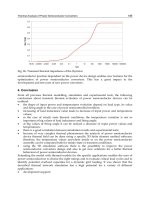
The evolution of the J-V light curves (Fig. 17) of all samples showed an increase of the
photovoltaic parameters by increasing the Freon partial pressure until 40mbar, while the J-V
characteristic of the sample F50 showed a decrease of the fill factor to 0.25. The latter
behavior could be related to a very strong intermixing between CdS and CdTe, due to the
treatment, so that a very large p-n junction region was present.
A clear roll-over behavior of all the J-V curves was observed in the Fig. 17; mainly for the
untreated sample and F20 and F50. This behavior was attributed to an n-p parasitic junction,
opposite to the main p-n junction created by the back contact. We assume that this behavior
was also strongly related to the incorporation of Cl impurities into CdTe. In our belief, the
increment of the photocurrent collection should be essentially due to an increment of the
(b)
(a)
Solar Cells – Thin-Film Technologies
230
photogenerated minority carriers lifetime in the CdTe layer which suggested that the
passivation of defects in absence of Cl contributed as non radiative recombination centers
(Consonni et al. 2006). We considered the 50mbar HCF
2
Cl cell an overtreated sample where
the intermixing process was so strong that all the available CdS was consumed. The
presence of shunt paths through the junction can explain the high reverse current and low
fill factor values.
The luminescence properties observed on the CdTe material showed a continuous increase
of the 1.4eV band intensity as a function of HCF
2
Cl partial pressure; the device electrical
characterization showed, on the contrary, a threshold at 40mbar partial pressure. Above this
value the solar cell performances collapsed dramatically suggesting a critical correlation
between HCF
2
Cl annealing and junction properties.
0 200 400 600 800 1000
-30
-20
-10
0
10
20
30
40
50
untreated
total pressure Ar 400 mbar
HCF
2
Cl 20mbar
HCF
2
Cl 30mbar
HCF
2
Cl 40mbar
HCF
2
Cl 50mbar
J (mA/cm
2
)
Voltage (V)
Fig. 17. Room temperature I-V characteristics under AM 1.5, 100mW/cm
2
illumination
conditions of untreated solar cells compared to the 20, 30, 40 and 50 mbar HCF
2
Cl partial
pressures respectively.
The comparison between the diode factor A and the 1.4eV intensity behaviors suggested
that the V
Cd
-Cl(F) complex was beneficial for the device performances, but did not explain
alone the maximum efficiency value measured for the 40 mbar annealed solar cells. A
combined CdTe material doping and grain boundaries passivation effect had to be invoked.
The absence of the 1.4eV band in the untreated and low HCF
2
Cl partial pressure annealed
CdTe after etching demonstrated that a non-radiative recombination centre was responsible
for the low A values. This centre was then passivated by the Cl (or F) incorporation till the
excess, for HCF
2
Cl partial pressures above 40 mbar, deteriorated the p-n junction.
The complex V
Cd
-Cl(F) formation could also be supported by the temperature dependent I-
V analyses carried out on the CdTe thin film. The Arrhenius plot extracted from the CdTe
dark conductivity as a function of the inverse of the temperature has been shown in Fig.18.
The plot showed that, in the case of untreated CdTe the high calculated activation energy
(324meV) has been related to a level due to the presence of occasional impurities like Cu, Ag
or Au; the activation energy decreases by increasing the HCF
2
Cl partial pressure, down to
E
a
=142meV for the material treated by 40mbar HCF
2
Cl partial pressure. This value was in
good agreement with those obtained in Cl (or F) doped CdTe single-crystals and attributed
to the A-centre, due to the complex V
Cd
-Cl(F) acceptor-like (Meyer et al. 1992).
Influence of Post-Deposition Thermal Treatment on the
Opto-Electronic Properties of Materials for CdTe/CdS Solar Cells
231
A model of the effect of annealing as a function of HCF
2
Cl partial pressure, on the bulk
CdTe and its grain boundaries as well as on the CdTe-CdS intermixing mechanisms
occurring at the interface has been showed in Fig. 19. The Cl (or F) impurities contained in
the annealing gas penetrate into the material partially doping the CdTe. The major part was
gettered to the grain boundaries, as observed in the monoCL image (Fig. 14 c), passivating
them and improving conductivity. Contemporary the interdiffusion of S in the CdTe and of
Te in CdS has been promoted by creating an intermixing region, which thickness increased
by increasing the HCF
2
Cl partial pressure, pictured by the orange region between CdTe and
CdS. The poor solar cell performances of the 50mbar HCF
2
Cl partial pressure annealed
device have been explained by a complete consumption of the CdS layer and by destruction
of the main p-n junction.
40 60 80 100 120 140
1x10
-13
1x10
-12
1x10
-11
1x10
-10
1x10
-9
(
-1
cm
-1
)
1/kT (eV
-1
)
30 mbar HCF
2
Cl
E
a
=201 meV
40 mbar HCF
2
Cl
E
a
=142 meV
untreated
E
a
=324 meV
Fig. 18. Temperature dependent I-V curves collected from the untreated, 30mbar and
40mbar HCF
2
Cl partial pressures respectively.
Fig. 19. Schematic representation of the effect of the HCF
2
Cl treatment on defects
distribution and intermixing junction formation
Solar Cells – Thin-Film Technologies
232
5. Conclusions
Thin films CdTe deposited by CSS have been submitted to a novel, full dry, post-deposition
treatment based on HCF
2
Cl gas. The annealing demonstrated to affect the structural
properties of the materials through the loss of preferential orientation. Texture coefficient of
the (111) Bragg reflection decreased from 2, for the untreated CdTe, down to 0.56 for the film
treated with the highest HCF
2
Cl partial pressure. On the contrary, the grain size did not
show any change after annealing maintaining an average dimension of about 12m. These
results were common for high temperature CSS deposited CdTe films, while a clear
dependence on the HCF
2
Cl partial pressure of the electro-optical properties of the films
have been observed through the presence of a 1.4 eV CL band in the annealed specimens.
The transition responsible for this emission involved an electronic level in the gap with an
energy of about 0.15 eV above the valence band edge, which could be attributed to a
complex between cadmium vacancy and an impurity probably identified in Cl or F (V
Cd
-
Cl/F) from the annealing gas.
The combined CL mapping and spectroscopy on single CdTe grains showed that the lateral
distribution of this complex was not homogeneous in the grain, but it was concentrated
close to the grain boundaries. The bulk grain, on the contrary, showed a high optical quality,
evidenced by the predominance of the NBE emission. The in-depth effectiveness of the
HCF
2
Cl annealing has been demonstrated by correlating depth-dependent CL analyses to
the study of the beveled CdTe surface due to the Br-methanol etching. High density of the
V
Cd
-Cl/F complex responsible for the 1.4 eV band has been observed close to the CdTe
surface; it decreased by increasing depth in the bulk region of the film about 5m below the
surface. By removing several microns of CdTe material and by approaching the CdTe/CdS
interface, in the etched specimens, an HCF
2
Cl partial pressure higher than 30 mbar was
necessary to detect the 1.4 eV emission, this means to create the V
Cd
-Cl/F complex. On the
other hand electrical characterization determined a threshold in the beneficial role of the
HCF
2
Cl annealing, showing the best solar cell performances for the 40 mbar partial pressure
treated device. Temperature dependent I-V analyses showed a remarkable decrease of the
electronic level activation energy, from 348meV to 142meV. The last value resulted in good
agreement with the energy values of the A-center found in the literature.
The comparison between the diode factor A and the 1.4 eV CL band intensity behaviors
evidenced that the V
Cd
-Cl/F complex was beneficial for the device performance, but does not
explain alone the maximum efficiency value measured for the 40 mbar annealed solar cells. A
tentative schematic model of the mechanisms occurring during post-deposition treatment, in
the bulk CdTe and close to the CdTe/CdS interface have been also proposed. A combined
CdTe-CdS intermixing and grain boundaries passivation effect has to be invoked.
6. References
Armani N., Salviati G., Nasi L., Bosio A., Mazzamuto S. and Romeo N., “Role of thermal
treatment on the luminescence properties of CdTe thin films for photovoltaic
applications”, (2007)
Thin Solid Films, vol. 515, pp. 6184-7, ISSN 00406090
Barret C. and Massalski T.B. Structure of Metals, edited by Pergamon, Oxford, p. 204 (1980)
Barrioz, V.; Lamb, D.A.; Jones; E.W. & Irvine, S.J.C. (2010). Suitability of atmospheric-pressure
MOCVD CdTe solar cells for inline production scale.
Materials Research Society
Symposium Proceedings;
ISBN: 978-160511138-4; San Francisco, CA; April 2009
Influence of Post-Deposition Thermal Treatment on the
Opto-Electronic Properties of Materials for CdTe/CdS Solar Cells
233
Bätzner, D.L.; Romeo, A.; Zogg, H.; Wendt, R. & Tiwari, A.N. (2001) Development of
efficient and stable back contacts on CdTe/CdS solar cells.
Thin Solid Films, Vol.387,
No.1-2, May 2001, pp. 151-154. ISSN: 00406090.
Birkmire, R.W.; Meyers, P.V. (1994) Processing issues for thin-film CdTe cells and modules,
Proceedings of the 24th IEEE Photovoltaic Specialists Conference, ISSN: 01608371,
Waikoloa, HI, USA, December 1994.
Bosio, A.; Romeo, N.; Mazzamuto, S. and Canevari V. (2006), Polycrystalline CdTe thin films
for photovoltaic applications.
Progress in Crystal Growth and Characterization of
Materials
, Vol.52, No.4, December 2006, pp. 247-279, ISSN: 09608974.
Aguilar-Hernandez J, Sastre-Hernandez J, Mendoza-Perez R, Cardenas-Garcia M and
Contreras-Puente G (2005), “Influence of the CdCl2 thermal annealing on the
luminescent properties of CdS-CSVT thin films”,
Physica Status Solidi C - Conference
and Critical Reviews
, vol. 2, No 10, p.p. 3710-3713, ISSN: 1610-1634
Chu, T.L.; Chu, S.S.; Ferekides, C.; Wu, C.Q.; Britt, J. & Wang, C. (1991). 13.4% efficient thin-
film CdS/CdTe solar cells.
Journal of Applied Physics, Vol.70, No.12, 1991, pp. 7608-
7612.
ISSN: 00218979
Compaan, A.D.; Tabory, C.N.; Li, Y.; Feng, Z. & Fischer, A. (1993). CdS/CdTe Solar cells by
RF sputtering and by laser physical vapor deposition.
Proceedings of the 23rd IEEE
Photovoltaic Specialists Conference,
pp. 394-399, ISBN: 0780312201, Louisville, KY,
USA; May 10-14, 1993
Consonni V., Feuillet G. and Renet S., (2006), “Spectroscopic analysis of defects in chlorine
doped polycrystalline CdTe”
J. Appl. Phys., vol. 99, p.p. 053502-1/7, ISSN: 0021-8979
Consonni V., Feuillet G., Bleuse j. and Donatini F., (2007) “Effects of island coalescence on
the compensation mechanisms in chlorine doped polycrystalline CdTe”,
J. Appl.
Phys
., vol. 101, p.p- 063522-1/6, ISSN: 0021-8979
Cruz, L.R.; Kazmerski, L.L.; Moutinho, H.R.; Hasoon, F.; Dhere, R.G. & De Avillez, R. (1999).
Influence of post-deposition treatment on the physical properties of CdTe films
deposited by stacked elemental layer processing.
Thin Solid Films, Vol.350, No. 1,
August 1999, pp. 44-48. ISSN: 00406090
Cunningham, D.; Davies, K.; Grammond, L.; Mopas, E.; O’Connor, M.; Rubcich, M; Sadeghi,
M.; Skinner, D. and Trumbly, T. (2000). Large area Apollo module performance and
reliability.
Proceedings of the 28th IEEE Photovoltaic Specialists Conference.
Enriquez, J.P. and Mathew, X. (2004). XRD study of the grain growth in CdTe films annealed
at different temperatures.
Solar Energy Materials and Solar Cells. Vol. 81, No. 3,
February 2004, pp. 363-369, ISSN: 09270248
Ferekides, C.S.; Marinskiy, D.; Viswanathan, V.; Tetali, B.; Palekis, V.; Selvaraj, P. & Morel,
D.L. (2000). High efficiency CSS CdTe solar cells.
Thin Solid Films. Vol.361,
(February 2000), pp. 520-526, ISSN: 00406090
Grillo V., Armani N., Rossi F., Salviati G. and Yamamoto N., (2003), “Al.L.E.S.: A random
walk simulation approach to cathodoluminescence processes in semiconductors”
Inst. Phys. Conf. Ser. No 180, p.p. 559-562, ISSN 0951-3248
Hartley, A.; Irvine, S.J.C.; Halliday, D.P. & Potter, M.D.G. (2001). The influence of CdTe
growth ambient on MOCVD grown CdS/CdTe photovoltaic cells.
Thin Solid Films.
Vol.387, No.1-2, May 2001, pp. 89-91. ISSN: 00406090
Hernández-Contreras, H.; Contreras-Puente, G. , Aguilar-Hernández, J. , Morales-Acevedo,
A. , Vidal-Larramendi, J. & Vigil-Galán, O. (2002). CdS and CdTe large area thin
films processed by radio-frequency planar-magnetron sputtering.
Thin Solid Films.
Vol.403-404, February 2002, Pages 148-152. ISSN: 00406090
Solar Cells – Thin-Film Technologies
234
Josell, D.; Beauchamp, C. R.; Jung, S.; Hamadani. B. H.; Motayed, A.; Richter, L. J.; Williams,
M.; Bonevich, J. E.; Shapiro, A. ; Zhitenev, N. & Moffat, T. P. (2009). Three
Dimensionally Structured CdTe Thin-Film Photovoltaic Devices with Self-Aligned
Back-Contacts: Electrodeposition on Interdigitated Electrodes.
Journal of
Electrochemical Society
. Vol.156, No.8, (June 2009). pp. H654-H660, ISSN: 0013-4651
Kosyachenko, L.A.; Mathew, X.; Motushchuk, V.V. & Sklyarchuk, V.M. (2006). Electrical
properties of electrodeposited CdTe photovoltaic devices on metallic substrates:
study using small area Au–CdTe contacts.
Solar Energy. Vol.80, No.2, (February
2006), pp. 148-155, ISSN: 0038092X
Krustok, J; Madasson, J; Hjelt, K, and Collan H (1997) “1.4 eV photoluminescence in
chlorine-doped polycrystalline CdTe with a high density of defects”
Journal of
Materials Science
, vol. 32 No: 6 p.p. 1545-1550, ISSN 00222461
Lane, D.W.; Rogers, K.D.; Painter, J.D.; Wood, D.A. & Ozsan, M.E. (2000). Structural
dynamics in CdS-CdTe thin films.
Thin Solid Films, Vol.361, February 2000, pp. 1-8.
ISSN: 00406090
Levy-Clement, C. (2008). Thin film electrochemical deposition at temperatures up to 180 °C
for photovoltaic applications.
Proceedings of Interfacial Electrochemistry and Chemistry
in High Temperature Media - 212th ECS Meeting;
ISBN: 978-160560312-4; Washington,
DC; October 2007
Lincot, D. (2005). Electrodeposition of chalcogenide semiconductors. Proceedings of 207th
Electrochemical Society Meeting,
Quebec, May 2005.
Luschitz, J.; Siepchen, B.; Schaffner, J.; Lakus-Wollny, K.; Haindl, G.; Klein, A. and
Jaegermann, W. (2009) CdTe thin film solar cells: Interrelation of nucleation,
structure, and performance.
Thin Solid Films, Vol. 517, No.7, February 2009, pp.
2125-2131, ISSN: 00406090.
McCandless, B.E. & Birkmire, R.W. (1991) Analysis of post deposition processing for
CdTe/CdS thin film solar cells.
Solar Cells, vol. 31, No. 6, December 1991, pp. 527-
535, ISSN: 03796787.
McCandless, B.E.; Moulton, L.V. and Birkmire, R.W. (1997). Recrystallization and sulfur
diffusion in CdCl
2
-treated CdTe/CdS thin films. Progress in Photovoltaics: Research
and Applications
, Vol. 5, No.4, July 1997, pp. 249-260, ISSN: 10627995.
McCandless, B.E. (2001). Thermochemical and kinetic aspects of cadmium telluride solar cell
processing.
MRS Proceedings, Vol.668, H1.6, ISSN: 02729172, San Francisco, CA,
USA; April 16-20, 2001
McCandless, B.E. & Sites, J.R. (2003) Cadmium telluride solar cells in:
Handbook of
Photovoltaic Science and Engineering
Luque, A. and Hegedus, S.S., pp. 617–662, John
Wiley & Sons Ltd, ISBN: 9780471491965, Chichester, UK.
McCandless, B.E. and Dobson, K.D. (2004). Processing options for CdTe thin film solar cells.
Solar Energy, Vol. 77, No.6, December 2004, pp. 839-856, ISSN: 0038092X.
Merano, M.; Sonderegger, S.; Crottini, A.; Collin, S.; Pelucchi, E.; Renucci, P.; Malko, A.;
Baier, M.H.; Kapon, E.; Ganiere, J.D. and Deveaud, B. (2006) Time-resolved
cathodoluminescence of InGaAs/AlGaAs tetrahedral pyramidal quantum
structures.
Applied Physics B: Lasers and Optics, Vol. 84, No.1-2, July 2006, pp. 343-
350, ISSN: 09462171.
Meyer BK, Stadler W, Hofmann DM, Ömling P, Sinerius D and Benz KW (1992), On the
Nature of the Deep 1.4 eV Emission Bands in CdTe - a Study with
Photoluminescence and ODMR Spectroscopy,
Journal of Crystal Growth, vol. 117, No
1-4, p.p. 656-659 ISSN: 0022-0248
Influence of Post-Deposition Thermal Treatment on the
Opto-Electronic Properties of Materials for CdTe/CdS Solar Cells
235
Moutinho, H.R.; Al-Jassim, M.M.; Levi, D.H.; Dippo, P.C. and Kazmerski, L.L. (1998). Effects
of CdCl
2
treatment on the recrystallization and electro-optical properties of CdTe
thin films.
Journal of Vacuum Science and Technology A: Vacuum, Surfaces and Films.
Vol.16, No.3, May 1998, pp. 1251-1257, ISSN: 07342101.
Moutinho, H.R.; Dhere, R.G.; Al-Jassim, M.M.; Levi D.H. and Kazmerski L.L. (1999).
Investigation of induced recrystallization and stress in close-spaced sublimated and
radio-frequency magnetron sputtered CdTe thin films.
Journal of Vacuum Science and
Technology A: Vacuum, Surfaces and Films.
Vol.17, No.4, 1999, pp. 1793-1798, ISSN:
07342101.
Paulson P.D. and Dutta V (2000). Study of in situ CdCl2 treatment on CSS deposited CdTe
films and CdS/CdTe solar cells,
Thin Solid Films,vol. 370, p.p. 299-306, ISSN
00406090
Perrenaud, J, Kranz, L; Buecheler S.; Pianezzi, F. and Tiwari, A.N. (2011). The use of
aluminium doped ZnO as trasparent conductive oxide for CdS/CdTe solar cells.
Thin Solid Films. Aricle in Press. ISSN: 00406090
Plotnikov, V., Liu, X., Paudel, N., Kwon, D., Wieland & K.A., Compaan, A.D. (2011). Thin-film
CdTe cells: Reducing the CdTe.
Thin Solid Films. Article in Press. ISSN: 00406090
Potlog, T.; Khrypunov, G.; Kaelin, M.; Zogg, H. & Tiwari, A.N. (2007). Characterization of
CdS/CdTe solar cells fabricated by different processes.
Materials Research Society
Symposium Proceedings,
ISBN: 978-155899972-5, San Francisco, CA; April 2007
Potter, M.D.G.; Halliday, D.P.; Cousins, M. & Durose, K. (2000). Study of the effects of varying
cadmium chloride treatment on the luminescent properties of CdTe/CdS thin film
solar cells.
Thin Solid Films, Vol.361, February 2000, pp. 248-252. ISSN: 00406090
Romeo, A.; Bätzner, D.L.; Zogg, H. & Tiwari, A.N. (2000). Recrystallization in CdTe/CdS.
Thin Solid Films. Vol.361 (February 2000), pp. 420-425, ISSN: 00406090
Romeo, A.; Buecheler, S.; Giarola, M.; Mariotto, G.; Tiwari, A.N.; Romeo, N.; Bosio, A. &
Mazzamuto, S. (2009). Study of CSS- and HVE-CdTe by different recrystallization
processes.
Thin Solid Films, Vol.517, No.7, February 2009, pp. 2132-2135. ISSN:
00406090
Romeo, N.; Bosio, A.; Tedeschi, R.; Romeo, A. & Canevari, V. (1999). Highly efficient and
stable CdTe/CdS thin film solar cell.
Solar Energy Materials and Solar Cells, Vol.58,
No.2, June 1999, pp.209-218. ISSN: 09270248
Romeo, N.; Bosio, A.; Canevari, V. & Podestà, A. (2004). Recent progress on CdTe/CdS thin
film solar cells.
Solar Energy, Vol.77, No.6, December 2004, pp. 795-801. ISSN:
0038092X
Romeo, N.; Bosio, A.; Mazzamuto, S.; Podestà, A. and Canevari, V. (2005). The Role of
Single Layers in the Performance of CdTe/CdS thin film solar cells.
Proceedings of
25th Photovoltaic Energy Conference and Exhibition,
Barcelona, Spain, June 2005.
Romeo, N.; Bosio, A.; Romeo, A.; Mazzamuto, S. & Canevari, V. (2006). High Efficiency
CdTe/CdS Thin Film Solar Cells Prepared by Treating CdTe Films with a Freon
Gas in Substitution of CdCl
2
. Proceedings of the 21
st
European Photovoltaic Solar Energy
Conference and Exhibition,
pp.1857-1860, ISBN 3-936338-20-5, Dresden, Germany,
September 4-8, 2006.
Romeo, N.; Bosio, A.; Mazzamuto, S.; Romeo, A. & Vaillant-Roca, L. (2007). “High efficiency
cdte/cds thin film solar cells with a novel back-contact”,
Proceedings of the 22
nd
European Photovoltaic Solar Energy Conference and Exhibition,
pp. 1919-1921, Milan;
Italy.
Solar Cells – Thin-Film Technologies
236
Romeo, N.; Bosio, A.; Romeo, A. & Mazzamuto, S. (2010). A CdTe thin film module factory
with a novel process.
Proceedings of 2009 MRS Spring Meeting; Vol.1165, pp. 263-273,
ISBN: 978-160511138-4, San Francisco, CA, USA; April 13-17, 2009
Schulz, D.L.; Pehnt, M.; Rose, D.H.; Urgiles, E.; Cahill, A.F.; Niles, D.W.; Jones, K.M.;
Ellingson, R.J.; Curtis, C.J.; Ginley, D.S. (1997). CdTe Thin Films from Nanoparticle
Precursors by Spray Deposition.
Chemistry of Materials. Vol.9. No.4, April 1997, pp.
889-900. ISSN: 08974756
Stadler, W.; Hoffmann, D.M.; Alt, H.C.; Muschik, T.; Meyer, B.K.; Weigel, E.; Müller-Vogt,
G.; Salk, M.; Rupp, E. and Benz, K.W. (1995) Optical investigations of defects in
Cd
1-x
Zn
x
Te, Physical Review B, vol.51, No.16 1995, pp. 10619-10630, ISSN: 01631829.
Sze, S. (1981).
Physics of Semiconductor Devices (2nd ed.), Wiley, ISBN:9780471143239, New
York.
Yacobi, B.G. & Holt, D.B. (1990)
Cathodoluminescence microscopy of inorganic solids, Plenum
Press, ISBN: 0306433141, New York and London.
Yi, X. & Liou, J.J. (1995). Surface oxidation of polycrystalline cadmium telluride thin films
for Schottky barrier junction solar cells.
Solid-State Electronics. Vol.38, No.6, (1995),
pp.1151-1154, ISSN: 00381101.
Yoshida, T. (1992). Analysis of photocurrent in screen-printed CdS/CdTe solar cells.
Journal of
the Electrochemical Society.
Vol.139, No.8, August 1992, pp. 2353-2357. ISSN: 00134651
Yoshida, T. (1995). Photovoltaic properties of screen-printed CdTe/CdS solar cells on
indium-tin-oxide coated glass substrates.
Journal of the Electrochemical Society.
Vol.142, No.9, September 1995, pp. 3232-3237. ISSN: 00134651
Wu, X.; Keane, J.C.; Dhere, R.G.; DeHart, C.; Duda, A.; Gessert, T.A.; Asher, S.; Levi, D.H.
and Sheldon, P. (2001 a). 16.5% efficient CdS/CdTe polycrystalline thin-film solar
cell,
Proceedings of the 17th E-PVSEC, München, Germany; October 2001.
Wu, X.; Asher, S.; Levi, D.H.; King, D.E.; Yan, Y.; Gessert, T.A. & Sheldon, P. (2001 b).
Interdiffusion of CdS and Zn
2
SnO
4
layers and its application in CdS/CdTe
polycrystalline thin-film solar cells.
Journal of Applied Physics, Vol.89, No.8, April
2001, pp. 4564-4569. ISSN: 00218979
Wu, X. (2004). High-efficiency polycrystalline CdTe thin-film solar cells.
Solar Energy. Vol.77,
No6, (December 2004), pp. 803-814, ISSN: 0038092X
Wu, X.; Zhou, J.; Duda, A.; Yan, Y.; Teeter, G.; Asher, S.; Metzger, W.K.; Demtsu, S.; Wei, S
Huai. & Noufi, R. (2007). Phase control of Cu
x
Te film and its effects on CdS/CdTe
solar cell.
Thin Solid Films, Vol.515, No.15 SPEC. ISS., May 2007, pp. 5798-5803,
ISSN: 00406090
Xiaonan Li,. Niles D. W,. Hasoon F. S,. Matson R. J, and Sheldon P. (1999). Effect of nitric-
phosphoric acid etches on material properties and back-contact formation of CdTe-
based solar cells.
J. Vac. Sci. Technol. A, vol. 17, No 3, p.p. 805-809 ISSN: 07342101.
Zanio, K.; Willardson R.K. & Beer, A.C. (1978).
Cadmium telluride. Volume 13 of
Semiconductors and semimetals. Cadmium telluride
, Academic Press, ISBN 0127521135,
9780127521138, London, UK
Zhou, J.; Wu, X.; Duda, A.; Teeter, G. & Demtsu, S.H. (2007). The formation of different
phases of CuxTe and their effects on CdTe/CdS solar cells.
Thin Solid Films, Vol.
515, No.18, June 2007, pp. 7364-7369, ISSN: 00406090
Zoppi, G.; Durose, K.; Irvine, S.J.C. & Barrioz, V. (2006). Grain and crystal texture properties
of absorber layers in MOCVD-grown CdTe/CdS solar cells.
Semiconductor Science
and Technology.
Vol.21, No.6, June 2006, pp. 763-770. ISSN: 02681242
11
Chemical Bath Deposited CdS for CdTe and
Cu(In,Ga)Se
2
Thin Film Solar Cells Processing
M. Estela Calixto
1
, M. L. Albor-Aguilera
2
, M. Tufiño-Velázquez
2
,
G. Contreras-Puente
2
and A. Morales-Acevedo
3
1
Instituto de Física, Benemérita Universidad Autónoma de Puebla, Puebla,
2
Escuela Superior de Física y Matemáticas, Instituto Politécnico Nacional, México,
3
CINVESTAV-IPN, Departamento de Ingeniería Eléctrica, México,
México
1. Introduction
Extensive research has been done during the last two decades on cadmium sulfide (CdS)
thin films, mainly due to their application to large area electronic devices such as thin film
field-effect transistors (Schon et al., 2001) and solar cells (Romeo et al., 2004). For the latter
case, chemical bath deposited (CBD) CdS thin films have been used extensively in the
processing of CdTe and Cu(In,Ga)Se
2
solar cells, because it is a very simple and inexpensive
technique to scale up to deposit CdS thin films for mass production processes and because
among other n-type semiconductor materials, it has been found that CdS is the most
promising heterojunction partner for these well-known polycrystalline photovoltaic
materials. Semiconducting n-type CdS thin films have been widely used as a window layer
in solar cells; the quality of the CdS-partner plays an important role into the PV device
performance. Usually the deposition of the CdS thin films by CBD is carried out using an
alkaline aqueous solution (high pH) composed mainly of some sort of Cd compounds
(chloride, nitrate, sulfate salts, etc), thiourea as the sulfide source and ammonia as the
complexing agent, which helps to prevent the undesirable homogeneous precipitation by
forming complexes with Cd ions, slowing down thus the surface reaction on the substrate.
CdS films have to fulfill some important criteria to be used for solar cell applications; they
have to be adherent to the substrate and free of pinholes or other physical imperfections.
Moreover, due to the requirements imposed to the thickness of the CdS films for the solar
cells, it seems to be a function of the relative physical perfection of the film. The better
structured CdS films and the fewer flaws present, the thinner the film can be, requirement
very important for the processing of Cu(In,Ga)Se
2
based thin film solar cells, thickness ~ 30 -
50 nm. In such case, the growth of the thin CdS film is known to occur via ion by ion
reaction, resulting thus into the growth of dense and homogeneous films with mixed
cubic/hexagonal lattice structure (Shafarman and Stolt, 2003).
The reason to choose the CBD method to prepare the CdS layers was due to the fact that
CBD forms a very compact film that covers the TCO layer, in the case of the CdTe devices
and the Cu(In,Ga)Se
2
layer without pinholes. Moreover, the CdS layer in a hetero-junction
solar cell must also be highly transparent and form a chemical stable interface with the
Solar Cells – Thin-Film Technologies
238
Cu(In,Ga)Se
2
and CdTe absorbing layers. The micro-crystalline quality of the film may also
be related to the formation of the CdZnS ternary layer in the case of the Cu(In,Ga)Se
2
and
CdS
1-x
Te
x
ternary layer for the case of CdTe, at the interface helping to reduce the effects
associated to the carrier traps in it. Hence, the deposition conditions and characteristics of
the CdS layer may affect strongly the efficiency of the solar cells. We have worked with this
assumption in mind for making several experiments that will be described in the following
paragraphs. As it will be shown, we have been able to prepare optimum CdS layers by CBD
in order to be used in solar cells, and have found that the best performance of CdS/CdTe
solar cells is related to the CdS layer with better micro-crystalline quality as revealed by
photoluminescence measurements performed to the CdS films.
2. CdS thin films by chemical bath deposition technique (CBD)
Chemical bath deposition technique (CBD) has been widely used to deposit films of many
different semiconductors. It has proven over the years to be the simplest method available
for this purpose, the typical components of a CBD system are a container for the solution
bath, the solution itself made up of common chemical reactive salts, the substrate where the
deposition of the film is going to take place, a device to control the stirring process and
temperature, sometimes a water bath is included to ensure an homogeneous temperature,
an schematic diagram of the CBD system is shown in figure 1. The concentrations of the
components of the solution bath for CdS can be varied over a working range and each group
use its own specific recipe, so there are as many recipes to deposit CdS as research groups
working in the subject. The chemical reactive salts are generally of low cost and in general it
is necessary to use small quantities. The most important deposition parameters in this
technique are the molar concentration, the pH, the deposition temperature, the deposition
time, the stirring rate, the complexing agents added to the bath to slowing down the
chemical reactions, etc. However, once they have been established these are easy to control.
The CdS thin film deposition can be performed over several substrates at a time, and the
reproducibility is guaranteed if the deposition parameters are kept the same every time a
deposition is done. Substrates can have any area and any configuration, besides they can be
of any kind, electrical conductivity is not required.
Fig. 1. Schematic diagram of a CdS chemical bath deposition system
Chemical Bath Deposited CdS for CdTe and Cu(In,Ga)Se
2
Thin Film Solar Cells Processing
239
Previously we have reported the preparation of monolayers and bi-layers of CdS deposited
by chemical bath deposition technique using a solution bath based on CdCl
2
(0.1 M), NH
4
Cl
(0.2 M), NH
3
(2 M) and thiourea (0.3 M), maintaining fixed deposition time and temperature
conditions and varying the order of application of the CdCl
2
treatment (Contreras-Puente et
al., 2006). Initially, the solution is preheated during 5 min prior to add the thiourea, after
that the deposition was carried out during 10 min at 75 C, then the second layer (the bi-
layer) was deposited at a lower deposition temperature, thus allowing us to control the
growth rate of the CdS layer. This was aimed to obtain films with sub-micron and
nanometric particle size that could help to solve problems such as partial grain coverage,
inter-granular caverns and pinholes. In this way, CdS thin films have been deposited onto
SnO
2
: F substrates of 4 cm
2
and 40 cm
2
, respectively.
Figure 2 shows the typical X-ray diffraction pattern obtained with a glancing incidence X-
ray diffractometer, for CdS samples prepared in small and large area, respectively. CdS
films grow with preferential orientation in the (002), (112) y (004) directions, which
correspond to the CdS hexagonal structure (JCPDS 41-049). Small traces of SnO
2
:F are
observed (*) in the X-ray patterns. Figure 3 shows the morphology for both mono and bi-
layers of CdS films, respectively. It can be observed that bi-layer films present lower pinhole
density and caverns. This is a critical parameter because it gives us the possibility to
improve the efficiency of solar cell devices. Several sets of CdTe devices were made and
their photovoltaic parameters analyzed, giving conversion efficiencies of 6.5 % for both
small and large area devices.
Fig. 2. X-ray diffraction patterns of mono and bi-layers of CdS
Also, we have found that the position of the substrate inside the reactor is an important
factor because the kinetics of the growth changes. Figure 4 shows how the transmission
response changes with substrate position inside the reactor. The deposition time for all
samples was 10 min. According to figure 4a when the substrates are placed horizontally at
the bottom of the reactor the CdS film grows a thickness of 150 nm, but the transmission
response is poor, when the substrates are placed vertically and suspended with a pair of
tweezers inside the reactor the CdS film grows a thickness of 110 nm and the transmission
response is 83% (see figure 4b), however in this configuration handling the substrate is
20 30 40 50 60 70 80 90
*
(112)
b
Bi-layer of CdS
(002)
(004)
*
*
*
Monolayer of CdS
Intensity (a.u.)
2Degrees)
a
Solar Cells – Thin-Film Technologies
240
complicated. Because of this, to design a better substrate holder/support was imperative.
So, a new support was designed and built to facilitate the access and handling of the
samples inside the reactor. Figures 4c and 4d shown the transmission response for mono
and bi-layers of CdS deposited using the new substrate support, placed in a vertical
configuration inside the reactor, for both cases the values were between 85 – 95 %, being the
monolayers the ones that exhibit the best response; however its morphology shows a larger
surface defect density. The thickness of these samples is in the order of 100 – 120 nm.
Fig. 3. SEM images of a monolayer and a bi-layer of CdS
Fig. 4. Transmission response of CdS films as a function of the position inside the reactor
2.1 CdS by CBD with a modified configuration
Figure 5 shows the implementation of the new substrate support for the CBD system, from
this figure it can be seen that the CBD system is the same as the one shown in figure 1 but
with the addition of the substrate holder. It basically holds the substrates vertically and
steady, while keeping it free to rotate along with the substrates, in such case the magnetic
stirrer is no longer needed. This substrate support can be set to rotate at different speed
rates, allowing the growth and kinetics of the reaction of CdS to change and in the best case
to improve, improving thus the physical properties of CdS films. The design includes a
400 600 800 1000
0
10
20
30
40
50
60
70
80
90
100
a
b
c
d
Transmitance (%)
Wavelength (cm
-1
)
Chemical Bath Deposited CdS for CdTe and Cu(In,Ga)Se
2
Thin Film Solar Cells Processing
241
direct current motor that has the option to vary the speed rate from 0 to 50 rpm. The motor
can move the substrate support made of a Teflon structure that holds up to 4 large area
substrates (45 cm
2
each). The principal advantage of using this modified structure is the
ability to handle 4 substrates at a time, placing them, inside the reactor containing the
solution bath and at the same time starting the rotation, by doing this all the CdS films are
expected to have a uniform growth and thickness 120 nm. When the substrate holder is set
to rotate inside the reactor, the kinetics of the CdS films growth was clearly affected as
shown in figure 6, it can be seen that when the rotating speed goes up, the transmission
Fig. 5. Schematic diagram of the new substrate holder for the CBD system
Fig. 6. Transmission response as a function of the rotation rate for CdS films prepared with
the new substrate holder.
300 400 500 600 700 800 900 1000
0
20
40
60
80
100
w/o rotation
35 rpm
52 rpm
Transmitance (%)
Wavelen
g
th
(
cm
-1
)
Solar Cells – Thin-Film Technologies
242
response decreases to 65% compared to the samples prepared without rotation. The
deposition time was set to 10 min in all cases, giving thus the growth of CdS films with 120 –
130 nm.
Fig. 7. SEM images of (a) mono and (b) bi-layer of CdS deposited at 35 rpm
Figure 7 shows the SEM images of CdS films prepared using the new substrate holder,
according to these images, the morphology of the mono and bi-layers of CdS changes as a
function of the rotating speed. Also we can clearly see an increase in the particle size for
each case, for the monolayer of CdS the particle size ball- like shape of 0.5 – 1 m, but
more uniform and compact compared to the particle size that the bi-layers of CdS exhibit
with rotation speed set to 35 rpm, flakes-like shape with size of 1 – 4 m. No devices have
been made so far using CdS films grown with this improved CBD system, studies are being
performed and research on the subject is ongoing in order to optimize the deposition
conditions, for this case.
3. Cu(In,Ga)Se
2
based thin films by co-evaporation technique (PVD)
Semiconducting CuInSe
2
is one of the most promising materials for solar cells applications
because of its favorable electronic and optical properties including its direct band gap with
high absorption coefficient (10
5
cm
-1
) thus layers of only 2 m thickness are required to
absorb most of the usable solar radiation and inherent p-type conductivity. Besides, the
band gap of CuInSe
2
can be modified continuously over a wide range from 1.02 to 2.5 eV by
substituting Ga for In or S for Se, which means that this material can be prepared with a
different chemical composition. Cu(In,Ga)Se
2
is a very forgiving material so high efficiency
devices can be made with a wide tolerance to variations in Cu(In,Ga)Se
2
composition
(Rocheleau et al., 1987 and Mitchell K. et al., 1990), grain boundaries are inherently passive
so even films with grain sizes less than 1 μm can be used, and device behavior is insensitive
to defects at the junction caused by a lattice mismatch or impurities between the
Cu(In,Ga)Se
2
and CdS. The latter enables high-efficiency devices to be processed despite
exposure of the Cu(In,Ga)Se
2
to air prior to junction formation. For Cu(In,Ga)Se
2
thin film
solar cells processing the substrate structure is preferred over the superstrate structure. The
substrate structure is composed of a soda lime glass substrate, coated with a Mo layer used
as the back contact where the Cu(In,Ga)Se
2
film is deposited. The soda lime glass, which is
used in conventional windows, is the most common substrate material used to deposit
Cu(In,Ga)Se
2
since it is available in large quantities at low cost. Besides, it has a thermal
expansion coefficient of 9 × 10
−6
K
-1
(Boyd et al., 1980) which provides a good match to the
Cu(In,Ga)Se
2
films. The most important effect of the soda lime glass substrate on
Chemical Bath Deposited CdS for CdTe and Cu(In,Ga)Se
2
Thin Film Solar Cells Processing
243
Cu(In,Ga)Se
2
film growth is that it is a natural source of sodium for the growing material. So
that, the sodium diffuses through the sputtered Mo back contact, which means that is very
important to control the properties of the Mo layer. The presence of sodium promotes the
growth of larger grains of the Cu(In,Ga)Se
2
and with a higher degree of preferred
orientation in the (112) direction. After Cu(In,Ga)Se
2
deposition, the junction is formed by
depositing a CdS layer. Then a high-resistance (HR) ZnO and a doped high-conductivity
ZnO:Al layers are subsequently deposited. The ZnO layer reacts with the CdS forming the
Cd
x
Zn
1-x
S ternary compound, which is known to have a wider band gap than CdS alone,
increasing thus the cell current by increasing the short wavelength (blue) response and at
the same time setting the conditions to make a better electric contact. Finally, the deposition
of a current-collecting Ni/Al grid completes the device. The highest conversion efficiency
for Cu(In,Ga)Se
2
thin film solar cells of 20 % has been achieved by (Repins et al., 2008)
using a three stages co-evaporation process. The processing of photovoltaic (PV) quality
films is generally carried out via high vacuum techniques, like thermal co-evaporation. This
was mainly the reason, we have carried out the implementation and characterization of a
thermal co-evaporation system with individual Knudsen cells MBE type, to deposit the
Cu(In,Ga)Se
2
thin films (see figure 8). The deposition conditions for each metal source were
established previously by doing a deposition profile of temperature data vs. growth rate.
The thermal co-evaporation of Cu(In,Ga)Se
2
thin films was carried out using Cu shots
99.999%, Ga ingots 99.9999%, Se shots 99.999% from Alfa Aeser and In wire 99.999% from
Kurt J. Lesker, used as received. The depositions were performed on soda lime glass
substrates with sputtered Mo with 0.7 m of thickness. The substrate temperature was >
500 C, temperature of source materials was set to ensure a growth rate of 1.4, 2.2 and 0.9
Å/s for Cu, In and Ga, respectively for the metals, while keeping a selenium overpressure
into the vacuum chamber during film growth.
Fig. 8. Thermal co-evaporation system with Knudsen effusion cells to deposit Cu(In,Ga)Se
2
thin films
Solar Cells – Thin-Film Technologies
244
Cu(In,Ga)Se
2
thin films were grown with different Ga and Cu ratios (Ga/(In+Ga) = 0.28,
0.34 and 0.35 respectively and Cu/(In+Ga) = 0.85, 0.83 and 0.94). The deposition time was
set to 30 min for all cases. All the Cu(In,Ga)Se
2
samples were grown to have 2 - 3 m
thickness and aiming to obtain a relative low content of gallium 0.30 % (CuIn
0.7
Ga
0.3
Se
2
),
while keeping the copper ratio to III < 1 (where III = In+Ga), very important criteria to use
them directly for solar cell applications, as shown in table 1. For solar cell devices, samples
JS17 and JS18 were used, with a chemical composition similar to that of sample JS13.
Chemical composition (at %) by EDS
Sample Cu In Ga Se Ga/III Cu/III
Reference 22.09 18.84 7.27 51.80 0.28 0.85
CIGS_5 21.27 16.73 8.88 53.69 0.35 0.83
CIGS_8 23.04 16.20 8.24 53.47 0.34 0.94
JS13 24.46 16.87 9.74 48.93 0.37 0.92
Table 1. Results of the chemical composition analysis of the co-evaporated Cu(In,Ga)Se
2
thin
films
The morphology of the Cu(In,Ga)Se
2
samples is very uniform, compact and textured,
composed of small particles (see figures 9a - 9c). Figure 9d shows the cross-section SEM
image and a film thickness 3.5 m, also notice the details of the textured surface of the
film, due to the high temperature processing.
Fig. 9. SEM micrographs of co-evaporated Cu(In,Ga)Se
2
thin films (a - c) and (d) cross
section image
The XRD patterns of the films show sharp and well defined peaks, indicating a very good
crystallization, the films appear to grow with a strong (112) orientation (see figure 10) and
with grain sizes ~ 1 µm. The expected shift of the (112) reflection compared to that of the
CuInSe
2
is also observed, which is consistent with a film stoichiometry of CuIn
0.7
Ga
0.3
Se
2
(JCPDS 35-1102).
Chemical Bath Deposited CdS for CdTe and Cu(In,Ga)Se
2
Thin Film Solar Cells Processing
245
Fig. 10. XRD pattern for Cu(In,Ga)Se
2
thin films thermal co-evaporated
4. CdTe thin films by Close Spaced Vapor Transport (CSVT)
CdTe is a compound semiconductor of II-VI type that has a cubic zincblende (sphalerite)
structure with a lattice constant of 6.481 A°.
CdTe at room temperature has a direct band
gap of 1.5 eV with a temperature coefficient of 2.3–5.4 x10
−4
eV/K. This band gap is an ideal
match to the solar spectrum for a photovoltaic absorber. Similarly to the Cu(In,Ga)Se
2
, the
absorption coefficient is large (around 5x10
4
cm
−1
) at photon energies of 1.8 eV or higher
(Birkmire R. and Eser E., 1997). Up to date the highest conversion efficiency achieved for
CdTe solar cells is 16.5% (Wu X. et al., 2001). CdTe solar cells are p-n heterojunction devices
in which a thin film of CdS forms the n-type window layer. As in the case of Cu(In,Ga)Se
2
-
based devices the depletion field is mostly in the CdTe. There are several deposition
techniques to grow the CdTe like, physical vapor deposition, vapor transport deposition,
close spaced sublimation, sputter deposition and electrodeposition (McCandless Brian E.
and Sites James R., 2003). In this case, the close spaced sublimation has been selected to
prepare the CdTe films for solar cell applications.
The sublimation technique for the deposition of semiconducting thin films of the II-VI group,
particularly CdTe, has proven to be effective to obtain polycrystalline materials with very
good optical and electrical properties. There are several steps that involve the formation of the
deposited materials, these are listed as follows: 1) synthesis of the material to be deposited
through the phase transition from solid or liquid to the vapor phase 2) vapor transport
between the evaporation source and the substrate, where the material will be deposited in the
form of thin film, and 3) vapor and gas condensation on the substrate, followed by the
nucleation and grow of the films. In general, and particularly in our CdTe - case, the vapor
transport is regulated by a diffusion gas model. This technique has several advantages over
others because is inexpensive, has high growth rates, and it can be scaled up to large areas for
mass production. The Close Spaced Vapor Transport technique, named as “CSVT”, is a variant
of the sublimation technique, it uses two graphite blocks, where independent high electrical
currents flow and due to the dissipation effect of the electrical energy by Joule’s heat makes the
temperature in each graphite block to rise. One of the graphite blocks is named the source
10 15 20 25 30 35 40 45 50 55 60
0
20
40
60
80
100
120
140
(301)
(213)
(211)
(103)
(312)
Mo (110)
(220/204)
Intensity x1000 (a.u.)
2 Theta (deg.)
Reference
CIGS_8
CIGS_5
(112)
(101)
CuIn
0.7
Ga
0.3
Se
2
PDF 35-1102
Solar Cells – Thin-Film Technologies
246
block and the other is the substrate block. Figure 11 shows the block diagram of the CSVT
system used to prepare the CdTe thin films. Between the source graphite block “A” and the
substrate graphite block “B” is located the graphite boat that contains the material to be
sublimated, and on top of this boat the substrate is located, in a very close proximity or close
spaced. The material growth is carried out under the presence of an inert atmosphere like
argon, nitrogen, etc. The growth rate of the material to be deposited can be controlled by
controlling the pressure and gas flow rate. Also this inert gas can be mixed with a reactive gas
like oxygen, which benefits the growth of CdTe with the characteristic p-type conductivity.
The deposition parameters for this technique are: a) T
s
: temperature of the source, b) T
sub
:
substrate temperature, it has to be lower than the T
s
in order to avoid the re-sublimation of the
material, c) d
s-sub
: distance between the material to be deposited and the substrate and d) P
g
:
pressure of the inert gas inside the chamber.
Fig. 11. Schematic diagram of a CSVT system
For the processing of CdTe thin film solar cells, it is necessary to use a superstrate structure,
so that the CdS is deposited on SnO
2
:F, in such a way that the growth process allows the
film to be deposited over the whole surface, becoming a surface free of holes and caverns
without empty spaces among the grains, and with a uniform grain size distribution. It is also
required that the CdS layer matches well with the CdTe host, thus favoring a good growing
kinetics for CdTe, as well as the formation of the CdS
x
Te
1-x
ternary compound in the
interface due to the diffusion of S from CdS to CdTe. The high-efficiency CdTe solar cells to
date have essentially the same superstrate structure. The superstrate structure is composed of
a sodalime glass substrate, coated with a SnO
2
:F; a transparent conductor oxide as the front
contact, then a CdS layer is chemically bath deposited, followed by the deposition of a CdTe
layer and finally the deposition of two layers of Cu and Au to form the back contact to
complete the CdS/CdTe device. In order to achieve solar cells with high conversion
efficiencies, the physical and chemical properties of each layer must be optimized (Morales-
Acevedo A., 2006). The deposition of CdTe was performed by using CdTe powder 99.999%
purity. The deposition atmosphere was a mixture of Ar and O
2
, with equal partial pressures
of O
2
and Ar. In all cases the total pressure was 0.1 Torr. Prior to all depositions the system
was pumped to 8×10
−6
Torr as the base pressure. In the CSVT-HW (hot wall) deposition, the
separation between source and substrate was about 1 mm. The deposition time was 3 min
for all the samples deposited with substrate and source temperatures of 550 °C and 650 °C,
respectively. Under these conditions, CdTe layers of 2 – 4 μm were obtained. The CdTe thin
films were also thermally treated with CdCl
2
. As discussed before, a very important
treatment independently of the deposition technique for both CdS and CdTe layers is a
thermal annealing after the deposition of CdCl
2
on top of the CdTe layer. If the CdCl
2
Chemical Bath Deposited CdS for CdTe and Cu(In,Ga)Se
2
Thin Film Solar Cells Processing
247
treatment is not performed, the short circuit current density and the efficiency of the solar
cell are very low. This treatment consists in depositing 300–400 nm of CdCl
2
on top of CdTe
with a subsequent annealing at 400 °C during 15–20 min in air, or in an inert gas atmosphere
like Ar. During this process the small CdTe grains are put in vapor phase and re-crystallize,
giving a better-organized CdTe matrix. The presence of Cl
2
could favor the CdTe grain
growth by means of a local vapor phase transport. In this way the small grains disappear
and the CdS/CdTe interface is reorganized.
5. Processing of Cu(In,Ga)Se
2
and CdTe thin films into solar cells
Cu(In,Ga)Se
2
and CdTe PV devices are obtained by forming p-n heterojunctions with thin
films of CdS. In this type of structure, n-type CdS, which has a band gap of 2.4 eV, not only
forms the p-n junction with p-type CuInSe
2
or p-type CdTe but also serves as a window
layer that lets light through with relatively small absorption. Also, because the carrier
density in CdS is much larger than in CuInSe
2
or CdTe, the depletion field is entirely in the
absorber film where electron-hole pairs are generated (Birkmire and Eser, 1997). After solar
cell completion the photovoltaic parameters like I
sc
, V
oc
, FF and conversion efficiency were
tested by doing the I-V characterization for the two structures; CdTe and Cu(In,Ga)Se
2
. All
the parameters were measured under AM1.5 illumination.
5.1 Cu(In,Ga)Se
2
/CdS thin film solar cells
The substrate structure of a Cu(In,Ga)Se
2
thin film based solar cell is composed of a soda
lime glass substrate, coated with a sputtered 0.7 – 1 m Mo layer as the back contact. After
the thermal co-evaporation of Cu(InGa)Se
2
deposition, the junction is formed by chemically
bath depositing the CdS with thickness 30 - 50 nm. Then a high-resistance (HR) ZnO layer
and a doped high-conductivity ZnO:Al layer are subsequently deposited, usually using the
sputtering technique. Finally, the deposition of a current-collecting grid of Ni/Al completes
the device as shown in figure 12. The total cell area is defined by removing the layers on top
of the Mo outside the cell area by mechanical scribing.
Fig. 12. Schematic configuration of a typical Cu(In,Ga)Se
2
thin film solar cell
5.1.1 Discussion on the Cu(In,Ga)Se
2
thin film based solar cells results
Two Cu(In,Ga)Se
2
samples were used to be processed into solar cell devices: sample JS17 had a
CdS layer prepared with a recipe based on CdCl
2
and sample JS18 with a recipe based on
CdSO
4
as the Cd source. The J-V parameters for devices JS17 are: area = 0.47 cm
2
, V
oc
= 536
mV, J
sc
= 31.70 mA/cm
2
, fill factor = 64.0 %, and = 10.9 % (see figure 13) and for JS18 are: area
Solar Cells – Thin-Film Technologies
248
= 0.47 cm
2
, V
oc
= 558 mV, J
sc
= 29.90 mA/cm
2
, fill factor = 63.1 %, and = 10.5 % (see figure 14).
From these results, we can see that sample JS17 shows a conversion efficiency a little bit higher
than JS18, this is due to the different recipe used to prepare the CdS layer as it was mentioned
before. This was the only difference between the two devices, everything else was the same.
From these figures, a low V
oc
is observed, but we should expect to have a higher V
oc
value,
compared to the Ga content. The roll-over in forward bias could be indicative of a low sodium
content in the Cu(In,Ga)Se
2
films. Also, the low current collection, observed for the
Cu(In,Ga)Se
2
thin film devices, may be due to incomplete processing of the absorber layer.
Improvements in device performance are expected with optimization of absorber processing.
Fig. 13. J-V curves for the best Cu(In,Ga)Se
2
thin film device prepared with a CdS bath
solution based on CdCl
2
Fig. 14. J-V curves for the best Cu(In,Ga)Se
2
thin film device prepared with a CdS bath
solution based on CdSO
4
5.2 CdTe/CdS thin film solar cells
The typical superstrate structure of a hetero-junction CdTe/CdS solar cell is composed of a
soda lime glass substrate, coated with a sputtered transparent conducting oxide (TCO) to the
visible radiation, which acts as the front contact, then a CdS layer with a thickness 120 nm is
chemically bath deposited, followed by the deposition of the absorber CdTe layer by close
spaced vapor transport technique and finally the CdS/CdTe device is completed by
depositing the ohmic back contact on top of the CdTe layer, see figure 15. For the back contact,
-50
-40
-30
-20
-10
0
10
20
30
40
50
-0.6 -0.4 -0.2 0.0 0.2 0.4 0.6 0.8 1.0
JS17-002
10.5% 10.9%
(a)
JS17
V(volts
)
J (mA/cm
2
)
-50
-40
-30
-20
-10
0
10
20
30
40
50
-0.6 -0.4 -0.2 0.0 0.2 0.4 0.6 0.8 1.0
JS18-004
10.2% 10.5%
(b)
JS18
V(volts)
J (mA/cm
2
)
Chemical Bath Deposited CdS for CdTe and Cu(In,Ga)Se
2
Thin Film Solar Cells Processing
249
two layers of Cu and Au (2nm and 350 nm, respectively) were evaporated, with an area of 0.08
cm
2
, onto the CdTe and annealed at 180 °C in Ar. The front contact was taken from the
conducting glass substrate (0.5 μm thick SnO
2
:F/ glass with sheet resistivity of 10 Ω/).
Fig. 15. Schematic configuration of a typical CdTe based solar cell
5.2.1 Variation of the S/Cd ratio in the solution for deposition of CdS by chemical bath
and its effect on the efficiency of CdS/CdTe solar cells
The variation of the S/Cd ratio in the solution used in the preparation of the CdS films
modifies the morphology, the deposition rate, the crystal grain size, the resistivity and the
optical transmittance of these films and have an influence upon the structural and electrical
properties of the CdTe layer itself, in addition to modifications of the CdS–CdTe interface.
Hence, our study shows the influence of the S/Cd ratio in the solution for CdS thin films
prepared by chemical bath upon the characteristics of CdS/CdTe solar cells with a
superstrate structure (Vigil-Galán, et al., 2005).
The concentrations of NH
3
, NH
4
Cl and CdCl
2
were kept constant in every experiment, but
the thiourea [CS(NH
2
)
2
] concentration was varied in order to obtain different S/Cd relations
(R
tc
) in the solution. All the films were grown on SnO
2
:F conducting glasses (10 ohm-cm) at
75 °C. Deposition times were also varied, according to our previous knowledge of the
growth kinetics (Vigil O. et al., 2001), with the purpose of obtaining films with similar
thickness in all cases. The selected thiourea concentrations and deposition times for each
S/Cd relation are shown in table 2.
S/Cd ratio
R
tc
Thiourea concentration
in the bath (mol/l)
Deposition time
(min)
1 2.4 x 10
-3
120
2.5 6 x 10
-2
100
5 1.2 x 10
-2
120
10 2.4 x 10
-2
120
Table 2. Thiourea concentration and deposition time for each S/Cd relation
Solar cells were prepared by depositing CdTe thin films on the SnO
2
:F/CBD-CdS substrates
by CSVT-HW. The atmosphere used during the CdTe was a mixture of Ar and O
2
, with an
O
2
partial pressure of 50%. In all cases, the total pressure was 0.1 Torr. Prior to deposition
the system was pumped to 8 × 10
−6
Torr as the base pressure. CSVT-HW deposition of CdTe
A
Sunlight
CdTe
CdS
SnO
2
:F
Soda-lime glass substrate
Au, 350 nm
Cu, 2 nm
Solar Cells – Thin-Film Technologies
250
was done by placing a CdTe graphite source block in close proximity (1 mm) to the
substrate block. The deposition time was 3 min for all the samples deposited with substrate
and source temperatures of 550 °C and 650 °C, respectively. Under these conditions, CdTe
layers of approximately 3.5 μm were obtained. The CdTe thin films were coated with a 200
nm CdCl
2
layer and then annealed at 400 °C for 30 min in air. For the back contact, two
layers of Cu and Au (2 nm and 350 nm, respectively) were evaporated, with an area of 0.08
cm
2
, on the CdTe film and annealed at 180 °C in Ar. The growth conditions of CdTe were
maintained constant for all solar cells.
5.2.2 Discussion on CdTe thin film solar cells results
Figure 16 shows the set of I–V characteristics for CdS/CdTe solar cells made with the same
R
tc
(S/Cd ratio = 5). According to our experimental conditions, the solar cells made with the
same technological process have similar characteristics.
Fig. 16. J –V characteristics of three CdS/CdTe solar cells made with CdS layers grown with
R
tc
= 5 during the CBD-CdS growth process
The I–V characteristics of CdS/CdTe solar cells under AM1.5 illumination (normalized to 100
mW cm
-2
) as a function of R
tc
are shown in figure 17. In table 3, the average shunt (R
p
) and
series (R
s
) resistances, the short circuit current density (J
sc
,), the open circuit voltage (V
oc
),
the fill factor (FF) and the efficiency (η) of solar cells prepared with different R
tc
are
reported. The averages were taken from four samples for each R
tc
. As can be seen in table 3,
η increases with R
tc
up to R
tc
= 5 and drops for R
tc
= 10.
S/Cd
ratio
R
tc
R
s
(ohm-cm
2
)
R
p
(ohm-cm
2
)
J
sc
(mA/cm
2
)
V
oc
(mV)
FF
(%)
(%)
1 6.8 318 20.8 617 55.2 7.1
2.5 5.4 800 21.8 690 55.5 8.3
5 2.9 787 23.8 740 70.5 12.3
10 5.9 135 22.7 435 52 5.4
Table 3. Photovoltaic parameter results for CdS/CdTe solar cells with different S/Cd ratio
(R
tc
) in the CdS bath
Chemical Bath Deposited CdS for CdTe and Cu(In,Ga)Se
2
Thin Film Solar Cells Processing
251
Fig. 17. Typical J –V characteristics of CdS/CdTe solar cells under illumination at 100 mW
cm
−2
, with R
tc
as a parameter
There are several factors directly or indirectly influencing the cell behaviour, in particular
the amount of S in the CBD CdS layers may influence the formation of the CdS
1-x
Te
x
ternary
compound at the CdS–CdTe interface. CdTe films grown at high temperatures, such as
those produced by CSVT, produce a sulfur enriched region due to S diffusion. The amount
of S penetrating the bulk of CdTe from the grain boundary must be dictated by the bulk
diffusion coefficient of S in CdTe and of course by the amount of S available in the CdS
films. The re-crystallization of CdTe could be affected by the morphological properties of
the CdS layers grown with different S/Cd ratios. These facts have been studied by Lane
(Lane D. W. et al., 2003) and Cousins (Cousins M. A. et al. 2003). From this point of view the
formation of CdS
1-x
Te
x
may be favored when the R
tc
is increased in the bath solution. This
ternary compound at the interface may cause a lower lattice mismatch between CdS and
CdTe, and therefore a lower density of states at the CdTe interface region will be obtained,
causing a lower value for the dark saturation current density J
0
. The resistivity of the CdS
and CdTe layers and their variation under illumination also change the characteristics of the
cell under dark and illumination conditions. In other words, a better photoconductivity
implies smaller resistivity values under illumination, with the possible improvement of the
solar cell properties. In addition, optical transmittance, thickness and morphological
measurements of the CBD-CdS films showed the following characteristics when increasing
R
tc
: i) band gap values are observed to increase (from 2.45 eV to 2.52 eV when changing R
tc
from 1 to 10), ii) grain sizes become smaller (from 55.4 nm to 47.2 nm when S/Cd = 1 and 10,
respectively) and iii) the average optical transmission above threshold increases from 68%
to 72% when R
tc
is increased from 1 to 10. Higher band-gap values of the window
material improve the short circuit current density of the solar cells. Thin films with
smaller grain sizes show fewer pinholes with a positive effect on the open circuit voltage
and fill factor. In this regard, the properties of the CdS layers are correlated with the
kinetic of the deposition process when the concentration of thiourea is changed. For
instance, for high thiourea concentration, the reaction rate becomes large enough to
promote a quick CdS precipitation which leads to the formation of agglomerates in the
solution rather than nucleation on the substrate surface, while for low thiourea
concentration a very slow growth process can be expected, leading to a thinner but more
homogeneous layer.
Solar Cells – Thin-Film Technologies
252
6. Conclusions
We have found that CBD-CdS thin films grown under different conditions, like monolayers
or bi-layers, using a standard bath configuration or a modified configuration, the principle
for the deposition process is the same: a common precipitation reaction. Depending of the
regime we decide to choose, we must perform an optimization of the deposition parameters
in order to get the CdS film with the best physical and chemical properties. The quality of
the CdS window partner and the absorber material like CdTe and Cu(In,Ga)Se
2
will have a
great impact on the conversion efficiencies when applied into thin film solar cells.
7. Acknowledgements
The authors would like to thank to Bill Shafarman from University of Delaware for device
processing and characterization. This work was partially supported by CONACYT, grant
47587, ICyT-DF, grant PICS08-54 and PROMEP, grant 103.5/10/4959.
8. References
Birkmire R. and Eser E. (1997), Annu. Rev. Mater. Sci., 27:625–53.
Boyd D, Thompson D, Kirk-Othmer, (1980), Encyclopaedia of Chemical Technology, Vol. 11,
3rd Edition, 807–880, John Wiley.
Contreras-Puente G., Tufino-Velazquez M., Calixto M. Estela, Jimenez-Escamilla M., Vigil-
Galan O., Arias-Carbajal A., Morales-Acevedo A., Aguilar-Hernandez J., Sastre-
Hernandez J., Arellano-Guerrero F.N. (2006), Photovoltaic Energy Conversion,
Conference Record of the 2006 IEEE 4th World Conference.
Cousins M. A., Lane D. W., and Rogers K. D. (2003). Thin Solid Films 431–432, 78.
Lane D. W., Painter J. D., Cousins M. A., Conibeer G. L., and Rogers K. D. (2003). Thin Solid
Films 431–432, 73.
McCandless Brian E. and Sites James R., (2003), Cadmium Telluride Solar Cells, in:
Handbook of Photovoltaic Science and Engineering, Luque A. and Hegedus S., pp.
567 – 616, John Wiley & Sons, Ltd ISBN: 0-471-49196-9, West Sussex, England.
Mitchell K. et al., (1990), IEEE Trans. Electron. Devices 37, 410–417.
Morales-Acevedo A. (2006). Solar Energy 80, 675.
Repins I. et al., (2008), Prog. in Photov: Research and Applications 16, 235.
Rocheleau R, Meakin J, Birkmire R, (1987), Proc. 19th IEEE Photovoltaic Specialist Conf., 972–976.
Romeo N., Bosio A., Canevari V. and Podestà A. (2004), Solar Energy, Volume 77, Issue 6,
Pages 795-801.
Shafarman W. N. and Stolt L. (2003), Cu(InGa)Se2 Solar Cells, in: Handbook of Photovoltaic
Science and Engineering, Luque A. and Hegedus S., pp. 567 – 616, John Wiley &
Sons, Ltd ISBN: 0-471-49196-9, West Sussex, England.
Schon, J. H., Schenker, O. and Batlogg, B. (2001), Thin Solid Films 385, p.271.
Vigil-Galan O., Arias-Carbajal A., Mendoza-Perez R., Santana-Rodríguez G., Sastre-
Hernandez J., Alonso J. C., Moreno-Garcia E., Contreras-Puente G. and Morales-
Acevedo A. (2005), Semiconductor Science and Technology 20, 819.
Vigil O., Arias-Carbajal A., Cruz F., Contreras-Puente G., and Zelaya-Angel O. (2001). Mats.
Res. Bull. 36, 521.
Wu X. et al., (2001), Proc. 17th European Photovoltaic Solar Energy Conf. 995.
12
Innovative Elastic Thin-Film
Solar Cell Structures
Maciej Sibiński and Katarzyna Znajdek
Technical University of Łódź, Department of
Semiconductor and Optoelectronic Devices,
Poland
1. Introduction
The idea of thin films dates back to the inception of photovoltaics in the early sixties. It is an
idea based on achieving truly low-cost photovoltaics appropriate for mass production,
where usage of inexpensive active materials is essential. Since the photovoltaic (PV)
modules deliver relatively little electric power in comparison with combustion-based energy
sources, solar cells must be cheap to produce energy that can be competitive. Thin films are
considered to be the answer to that low-cost requirement [1].
Replacement of single crystalline silicon with poly and amorphous films, caused the decline
of material requirements, which has led to lower final prices [2]. Furthermore, the thickness
of cell layers was reduced several times throughout the usage of materials with higher
optical absorption coefficients. Unique, thin film and lightweight, devices of low
manufacturing costs and high flexibility, were obtained by applying special materials and
production techniques, e.g. CIS, CIGS or CdTe/CdS technologies and organic elements.
Taking advantage of those properties, there is a great potential of new, useful applications,
such as building integrated photovoltaics (BIPV), portable elastic systems or clothing and
smart textiles as well [3].
Low material utilization, mass production and integrated module fabrication are basic
advantages of thin film solar cells over their monocrystalline counterparts [4]. Figure 1 (by
NREL) shows the development of thin film photovoltaic cells since 1975.
The development of cadmium telluride (CdTe) based thin film solar cells started in 1972
with 6% efficient CdS/CdTe [5] to reach the present peak efficiency of 16.5% obtained by
NREL researchers in 2002 [6]. Chalcopyrite based laboratory cells (CIS, CIGS) have recently
achieved a record efficiency of 20% [7], which is the highest among thin film PV cells (see
Table 1). Solar modules based on chalcopyrites, uniquely combines advantages of thin film
technology with the efficiency and stability of conventional crystalline silicon cells [4].
Thin film solar cell type
CIGS CdTe/CdS a-Si
Cell area [cm
2
] 0.5 1.0 0.25
Highest efficiency [%] 20.0 16.5 13.3
Typical efficiency range [%] 12.0 – 20.0 10.0 – 16.5 8.0 – 13.3
Table 1. Efficiencies of CIGS, CdTe and a-Si thin film solar cells [8].