Ferroelectrics Applications Part 7 pptx
Bạn đang xem bản rút gọn của tài liệu. Xem và tải ngay bản đầy đủ của tài liệu tại đây (4.13 MB, 23 trang )
Future Memory Technology and Ferroelectric Memory as an Ultimate Memory Solution
127
cell structures but also by certain aspects of its performance. To circumvent cell-to-cell
interference, width of a floating gate tends to be more aggressively squeezed than space
between floating gates (See Fig. 3b). This seems to result in a high aspect ratio of a gate stack.
Such a high aspect ratio can provoke fabrication difficulty of memory cells due to its
mechanical instability. And stored charge (e.g., electron) in a floating gate can redistribute
easily in operational conditions, leading to vulnerability of poor data retention. Since the
interference originates from another type of coupling between floating gates (FGs), it is
desirable to find innovative structures, where charge storage media do not have a form of
continuum of charge like the floating gate style but have a discrete sort such as charge traps
(CTs) in a nitride layer. The typical examples are non-volatile memories with non-floating
gate, for example, SONOS (silicon-oxide-nitride-oxide-silicon) (Mori et al., 1991), SANOS
(silicon-alumina-nitride-oxide-silicon) (Lee et al., 2005), TANOS (TaN-alumina-nitride-oxide-
silicon) (Shin et al., 2006) or nano-crystal dots (Tiwari et al., 1995; Nakajima et al., 1998).
Recently, 32 Gb flash memory has been reported, in particular, in 40 nm of technology node
(Park et al., 2006). They have pioneered a novel structure with a high-
κ
dielectric of Al
2
O
3
as
the top oxide and TaN as a top electrode. With this approach, they can achieve several
essential properties for NAND flash memory: reasonable programming/erasing
characteristics, an adequate V
PASS
window for multi-bit operation and robust reliability. It is
noteworthy that a TANOS structure has much better mechanical stability than that of an FG-
type cell because of the far lower stack in height. Interference among TANOS cells hardly
occurs due to nature of the charge trap mechanism−SiN (silicon nitride) traps act as point
charges. This is the biggest advantage in CT-NAND flash memory. To scale NAND flash
further down, we may need another cell technology. A FinFET could be a very promising
candidate because it can increase storage electrons effectively by a way of expanding channel
width of cell transistors, similar to 3-D CATs in DRAM. In this pursuit, a research group has
successfully developed flash memory with a TANOS structure based on a 3-D, body-tied
FinFET (Lee et al., 2006), where they can obtain excellent performance of NAND-flash cells
with robust reliability. If there are much higher
κ
dielectrics than Al
2
O
3
, then we can further
scale down the FinFET CT-NAND flash memory.
Fig. 4. (a) A schematic diagram of 3-D, body-tied FinFET NAND cells and (b) comparisons
of the 3-D cells with 2-D, planar cells in threshold-voltage shift as a function of programmed
threshold voltage, measured after suffering 5k program/erase cycles and a bake at 200 °C
for 2 hours (Lee et al., 2006).
Ferroelectrics - Applications
128
Figure 4 represents (a) a schematic diagram of 3-D, body-tied FinFET NAND cells and (b)
comparisons of the 3-D cells with 2-D ones in threshold-voltage shift as a function of
programmed threshold voltage, measured after suffering 5k program/erase cycles and a
bake at 200 °C for 2 hours. The threshold-voltage delay has been improved to 0.32 V in 3-D
NAND cells, compared with 2-D NAND ones.
2.2 Prospects of silicon technology
As well aware that the era of 2-D, planar-based shrink technology is coming to an end,
semiconductor institutes have seen enormous hurdles to overcome in order to keep up with
the Moore’s doubling pace and thus to meet the requirements of highly demanding
applications in mobile gadgetry. They have attempted to tackle those barriers by smart and
versatile approaches of 3-D technology in integration hierarchy. One strand of the responses
is to modify structures of elementary constituents such as DRAM’s CATs, its storage
capacitors and storage transistors of flash memory to 3-D ones from the 2-D. A second
thread revisits these modifications to a higher level of integration: memory stacking. And
another move is to upgrade this into a system in a way of fusing of each device in
functionality by utilizing smart CMOS technology, e.g., through-silicon-via (TSV).
2.2.1 Elementary level of 3-D approach
When working with silicon devices, a transistor’s key parameters must take into account:
on-current; off-leakage current; the number of electrons contained in each transistor; or the
number of transistors integrated. All of these factors are very important, but not equally
important in functional features of silicon devices. For instance, for memory devices, off-
leakage current is regarded as a more important factor and thus memory technologies tend
to be developed with a greater emphasis on reducing off-leakage current. For logic,
transistor delay is the single most important parameter, not just to indicate chip
performance but to measure a level of excellence in device technology as well. This
transistor delay is related closely to transistor’s on-current state. And with 2-D planar
technology in logic, one can continue to reduce transistor’s channel length down to 40 nm.
However, at less than 30 nm, the transistor begins to deviate in spite of a much relaxed off-
current requirement. This is because of non-scalable physical parameters such as mobility,
sub-threshold swing and parasitic resistance. To resolve these critical issues, two attempts
have been examined. One is to enhance carrier mobility by using mobility-enhancement
techniques such as strained silicon (Daembkes et al., 1986), SiGe/Ge channel (Ghani et al.,
2003), or an ultra thin body of silicon (Hisamoto et al., 1989), where carrier scattering is
suppressed effectively. Another approach is to reduce channel resistance by widening
transistor’s width. In this case, it appears very promising to use different channel structures
such as tri-gate (Chau et al., 2002) or multi channel (Lee et al., 2003b). We have witnessed
that, with 3-D FinFETs in memory devices, this attempt is very efficient for extending
incumbent shrink technology down to 30 nm of technology node. As silicon technology
scales down further, the two will eventually be merged into one single solution for an
optimum level of gate control. With this type of structure, one will arrive at nearly ideal
transistor performance such as being virtually free from the SCE, sufficient on-current and
suppressed off-leakage current. Figure 5 shows (a) evolution trends of logic transistors in
terms of EOT: A sharp decrease in EOT trend appears due to lack of gate controllability in 2-
D planar structures despite high-
κ
dielectrics. By contrast, those in 3-D, multi-gate structures
Future Memory Technology and Ferroelectric Memory as an Ultimate Memory Solution
129
are expected to have the same trend of EOT as those with conventional SiON dielectrics.
This suggests that 3-D structures seem to become essential even with high-
κ
materials. It is
thus believed that developing a 3-D transistor with either a multi-gate or an gate-all-around
structure (Colinge et al, 1990) is quite feasible if one can extend 2-D planar technology to 3-
D. This is because the channel length is no longer restricted by lateral dimension. Figure 5
also shows (b) a cross-sectional TEM (transmission-electron-micrograph) image of one of the
3-D, multi-gate transistors and (c) its Ion-Ioff characteristics are compared with those of 2-D
planar structures.
Fig. 5. (a) Equivalent-oxide-thickness (EOT) scaling trends (Kim, 2010) are shown in
reciprocal scale. Due to the difficulty in controlling the SCE, a sharp decrease in EOT trend
is inevitable for the coming nodes. However, the historical trend can be reverted back in the
case of 3-D, multi-gate transistors. (b) A cross-sectional TEM image of a 3-D, multi-gate and
(c) its Ion-Ioff characteristics are compared with those of the planar (Lee et al., 2003b).
2.2.2 3-D stacking of memory cells
New silicon technology based on 3-D integration has drawn much attention because it
seems to be regarded as one of the practical solutions. Though the concept of 3-D integration
was first proposed in the early 1980’s (Kawamura et al., 1983; Akasaka & Nishimura, 1986),
it has never been thoroughly investigated or verified until now, as neither silicon devices
approached their limits at those times nor high-quality silicon crystal was ready for
fabrication. Recent advances both in selective epitaxial silicon growth at low temperature
(Neudeck et al., 2000) and in high quality layer-transferring technology with high-precision
processing (Kim et al., 2004b), can bring major new momentum to the silicon industry via 3-
D integration technology. The simplicity of memory architecture consisting of memory
array, control logic and periphery logic, makes it relatively easy to stack one-memory cell
array over another. This will ultimately lead to multiple stack designs of many different
memories. Recently, one of the memory manufacturers has started to implement 3-D
integration technology with SRAM to reduce large cell-size (Jung et al., 2004). Figure 6
Ferroelectrics - Applications
130
shows (a) a cross-sectional TEM image of 3-D stacking SRAM (Left) and its schematic
diagram (Right) (Jung et al., 2004): Since transistors stacked onto a given area do not need to
isolate p-well to n-well, SRAM-cell size of 84 F
2
is being reduced to the extremely small cell
size of 25 F
2
. Encouraged by this successful approach, stacked flash memory has also been
pursued. Figure 6 also represents (b) 3-D stacking NAND flash memory (Jung et al., 2006):
This suggests great potential of 3-D memory stacking for large-scale use with 3-D flash-cell
technology, which will spur further growth in high-density applications. Beyond 20 nm
node, we believe that the most plausible way to increase density is to stack the cells
vertically. Figure 6 displays (c) a 3-D schematic view of vertical NAND flash memory
(Katamura et al., 2009), where SG is selecting gate, CG is control gate and PC is pipe
connection. The stacking of memory cells via 3-D technology looms on the horizon, in
particular, for NAND flash memory.
Fig. 6. (a) A cross-sectional TEM image of 3-D stacking SRAM (Left) and its schematic
diagram (Right) (Jung et al., 2004). (b) 3-D stacking NAND flash memory (Jung et al., 2006).
(c) A 3-D schematic view of vertical NAND flash memory (Katsumata et al., 2009), where SG
is selecting gate; CG is control gate; and PC is pipe connection. (d) A cross-sectional SEM
image of memory array after the removal of the sacrificial film (See Katsumata et al., 2009)
It is also believed that logic technology will shift to 3-D integration after a successful
jumpstart in silicon business. The nature of a logic device, where transistors and
interconnections are integrated as key elements, is not much different from those of stacked
memory cells. It may be very advantageous to introduce 3-D integration technology to a
logic area. Note that implementation of interconnection processes seems to be more efficient
in vertical scale. For example, a dual or quad-core CPU can be realized with only a half or
quarter of the chip size, which will result in significantly greater cost-effectiveness. Another
promising use would be to improve logic performance by cutting down on the length of
metallization. Decrease in interconnection length means a huge amount of reduction in
parasitic RC components, i.e., a high speed and power saving. In addition, 3-D technology
will make it easy to combine a memory device and a logic device onto one single chip
Future Memory Technology and Ferroelectric Memory as an Ultimate Memory Solution
131
through hierarchical stacking. Since most parts of SoCs (system-on-chips) in the future will
be allocated to memory, this combining trend will be accelerated. The next step will be to
stack multi-functional electronics such as RF (radio frequency) modules, CISs (CMOS image
sensors) and bio-sensors over the logic and memory layers.
2.2.3 Chip level of 3-D integration
The early version of 3-D integration in chip level has been commercialized already in a
multi-chip package (MCP), where each functional chip (not device) is stacked over one
another and each chip is connected by wire bonding or through the ‘through-via hole’
bonding method within a single package. Figure 7 exhibits (a) a bird’s eyes view of multi-
chip-package (MCP) by wire bonding; (b) wafer-level stack package with through-via-hole;
(c) a photograph of 3-D integrated circuit; and (d) a schematic drawing of a 3-D device for
use in medical applications. The advantages of the MCP are a small footprint and better
performance compared to a discrete chip solution. It is expected that the MCP approach will
continue to evolve. However, the fundamental limitation of MCP will be lack of cost-
effectiveness due to a number of redundancy/repair requirements. In this respect, ‘through-
silicon-via’ (TSV) technology is able to overcome MCP limitations through an easy
implementation of redundancies and repairs. Many groups have reported TSV-based
integrated circuit (TSV IC), where a single integrated circuit is built by stacking silicon
wafers or dies and interconnecting them vertically so that they can function as one single
device (Topol et al., 2006; Arkalgud, 2009; Chen et al., 2009). In doing so, key technologies
include TSV formation, wafer-thinning capability, thin wafer handling, wafers’ backside
processes, and 3D-stacking processes (e.g., die-to-die, die-to-wafer and wafer-to-wafer). In
detail, there are many challenging processes such as etching profiles of TSV sidewall, poor
isolation liners and barrier-deposition profiles. All of these are likely to provoke TSV’s
reliability concerns due to lack of protection from metal (e.g., Cu) contamination. A report of
silicon-based TSV interposers (Rao et al., 2009) may have advantages over traditional PCB or
ceramic substrate in that it has a shorter signal routing. This results from vertical
interconnect and improved reliability due to similarity to silicon-based devices in thermal
expansion and extreme miniaturization in volume. TSV-IC technologies together with the 3-
D interposers will accelerate an adoption of 3-D system-in-package (SiP) with heterogeneous
integration (See Fig. 7d). And this might be a next momentum for genuine 3D IC devices in
the future because of tremendous benefits in footprint, performance, functionality, data
bandwidth, and power. Besides, as the use of 3-D silicon technology has great potential to
migrate today’s IT devices into a wide diversification of multi-functional gadgetry, it can
also stimulate a trend that merges one technology with another, ranging from new materials
through new devices to new concepts. In this regard, new materials may cover the followings:
carbon nano-tube (CNT) (Iijima, 1991), nano-wire (NW) (Yanson et al., 1998), conducting
polymer (Sirringhaus et al. 1998), and molecules (Collier et al., 1999). New devices could
also be comprised of many active elements, such as tunneling transistors (Auer et al., 2001),
spin transistors (Supriyo Datta & Biswajit Das, 1990), molecular transistors (Collier et al.,
1999), single electron transistors (SETs) (Fulton & Dolan, 1987) and others. We may be able
to extend this to new concepts, varying from nano-scale computing (DeHon, 2003) and FET
decoding (Zhong et al., 2003) to lithography-free addressing (DeHon et al., 2003). To a
certain extent, some of these will be readily integrated with 3-D silicon technologies. This
integration will further enrich 3-D silicon technologies to create a variety of new multi-
functional electronics, which will provide further substantive boosts to silicon industry,
allowing us to make a projection of a nano-silicon era into practical realities tomorrow.
Ferroelectrics - Applications
132
Fig. 7. (a) A bird’s eyes view of (a) multi-chip-package (MCP) by wire bonding. (b) Wafer-
level stack package with through-via-hole. (c) A Photograph of 3-D integrated circuit. (d) A
schematic drawing of a 3-D device for medical applications enabled by TSVs and silicon
interposers.
These realities will be manifested in highly desirable applications of combining of information
technology (IT), bio-technology (BT), and nano-technology (NT), to become so called fusion
technology (FT). Given that key obstacles to realize this are tackled by bridging the gap
between previously incompatible platforms in silicon-based CMOS technology and new
technological concepts, a vast number of new applications will unfold. One example may be
many applications related to health sensor technology, in particular, the early recognition of
cancer diseases and the screening of harmful and poisonous elements pervasive in the
environment. Further, when a nano-scale bio-transistor is available, lab-on-a-chip (LoC) will
become a single solution integrating all of its essential components, such as micro-array,
fluidics, sensors, scanners and displayers. Then, by its very nature
8
, one will have tons of
benefits from a mass of disposable LoCs, which will stimulate the future silicon industry.
8
As a successful booster for the silicon industry, whatever will be, it should be a high volume product at
a reasonable price. PCs are high volume products, and hand-held phones are too. In that sense, LoC is
very promising because its potential market is the entire population.
Future Memory Technology and Ferroelectric Memory as an Ultimate Memory Solution
133
2.3 Remarks
Not only do many challenges await silicon industries as technology enters the deep nano-
dimension era but promising opportunities are also there. Equipped with new technologies
such as 3-D scaling and a wealth of new materials, alongside fusing of related technologies,
we will overcome many hurdles ahead and respond technological challenges we will
stumble along the way. All plausible solutions described earlier tell us that planar-based
technology will reach an impassable limit. 3-D technology begins to provide clear signs of
serving as a foundation for a refuel of the silicon industry. The advantages of 3-D
integration are numerous. They include: elimination of uncertainty in the electrical
characteristics of deep nano-scale transistors; extendable use of silicon infrastructures,
especially optical lithography tools; and formation of a baseline for multi-functional
electronics and thus facilitation of implementing a hierarchical architecture, where each
layer is dedicated to a specific functional purpose. Over the next decade, we will see great
endeavors in numerous areas that will greatly stimulate the semiconductor business.
Successful evolutions of device structures will continue and even accelerate at a greater pace
in the not-too-distant future. In addition, device designs will converge onto a single mobile
platform, covering many different capacities and services from telecommunication through
broadcasting and a much higher degree of data processing. In line with this, silicon
technology will still play a critical role in realizing functionally merged solutions. All of
these will permit us to have invaluable clues not just on how to prepare future silicon
technology but also on how to positively influence the entire silicon industry. This will
allow us to attain an even more sophisticated fusing of technologies. As seen in the past,
silicon technology will continue to provide our society with versatile solutions and as-yet
unforeseen benefits in much more cost-effective ways.
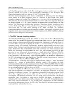
3. Ferroelectric memory as an ultimate memory solution
3.1 Introduction
There has been great interest to understand ferroelectric properties from the point of view of
both fundamental physics and the need of nano-scale engineering for memory devices. On
the one hand, since electric hysteresis in Rochelle salt was in 1920 discovered by Valasek
(Valasek, 1921), there have been tremendous efforts to look through ferroelectricity in a
comprehensive way over the past many decades. As a consequence, the phenomenological
theory of ferroelectricity has been presented by many researchers: Devonshire (Devonshire,
1949; Devonshire, 1951); Jona and Shirane (Jona and Shirane, 1962); Fatuzzo and Merz
(Fatuzzo and Merz, 1959); Line and Glass (Line and Glass, 1979); and Haun (Haun, 1988).
The series of their works have been successful to express the internal energy of a
ferroelectric crystal system. This theory has also been examined experimentally in detail,
and extended by Merz (Merz, 1953); by Drougard et. al. (Drougard et al., 1955); and by
Triebwasser (Triebwasser, 1956). Especially, Devonshire’s phenomenological theory
(Devonshire, 1949; Devonshire, 1951) gives the free energy of BaTiO
3
as a function of
polarization and temperature. From this free energy we know what the possible state and
meta-stable states of polarization are in the absence of an applied field. We also know how
polarization changes as a function of field applied to the crystal. In short, according to the
theory, a ferroelectric possesses two minima (e.g., a second-order phase transition) in the
internal energy. These two minima are separated by an energy barrier
Δ
E. Essential feature
of a ferroelectric is that these two minima corresponds to two different spontaneous
Ferroelectrics - Applications
134
polarizations that can be changeable reversibly by an applied field. Under an assumption
that applied electric field is able to surmount the energy barrier, the advent of smart thin-
film technology in evolution of CMOS technology, has enabled to consider a ferroelectric
crystal a useful application. Thinning a ferroelectric film with high purity means that there
could be an opportunity to use ferroelectrics as a memory element.
On the other, integrated ferroelectrics are a subject of considerable research efforts because
of their potential applications as an ultimate memory device due to 3 reasons: First, the
capability of ferroelectric materials to sustain an electrical polarization in the absence of an
applied field, means that integrated ferroelectric capacitors are non-volatile. They can retain
information over a long period of time without a power supply. Second, the similar
architectural configuration of memory cell-array to conventional ones, means that they are
highly capable of processing massive amounts of data. Finally, nano-second speed of domain
switching implies that they are applicable to a high-speed memory device. Since ferroelectric
capacitors was explored for use in memory applications by Kinney et al. (Kinney et al.,
1987); Evans and Womack (Evans & Womack, 1988); and Eaton et al. (Eaton et al., 1988), it
has been attempted to epitomize ferroelectrics to applicable memory solutions in many
aspects. In the beginning of 1990’s, silicon institutes have begun to exploit ferroelectrics as
an application for high-density DRAMs (Moazzami et al., 1992; Ohno et al., 1994). This is
because permittivity of ferroelectrics is so high as to achieve DRAM’s capacitance extremely
high and thus appropriate for high density DRAMs. An early version of non-volatile
ferroelectric RAM (random-access-memory) used to be several kilo bits in packing density.
This lower density (NB. at that moment, DRAM had several ten mega bits in density) is
because of two: One is that its memory unit was relatively large in size, being comprised of
two transistors and two capacitors (2T2C) to maximize sensing signal. The other is that a
ferroelectric capacitor stack has required not only novel metal electrodes such as platinum,
iridium and rhodium, all of which are hard to be fine-patterned due to processing hardness,
but also reluctant metal-oxide materials to conventional CMOS integration due to possible
cross contaminants such as lead zircornate titanate (PbZrTiO
3
) and strontium bismuth
titanate (Sr
1-x
Bi
x
TiO
3
). Next steps for high density non-volatile memory have been
forwarded (Tanabe et al., 1995; Sumi et al., 1995; Song et al., 1999). In similar to DRAM, an
attempt to build smaller unit cell in size was in the late 1990’s that one transistor and one
capacitor (1T1C) per unit memory was developed (Jung et al., 1998). Since then, many
efforts to build high density FRAM have been pursued, leading to several ten mega bits in
density during the 2000s (Lee et al., 1999; Kim et al., 2002; Kang et al., 2006; Hong et al., 2007;
Jung et. al, 2008).
Fig. 8. (a) Evolution of electronic components in data throughput performance. (b) NVM
(non-volatile memory) filling price/performance gap.
Future Memory Technology and Ferroelectric Memory as an Ultimate Memory Solution
135
Among integrated ferroelectrics, one of the most important parameters in FRAM is sensing
signal margin. The sensing signal of FRAM is proportional to remanent polarization (P
r
) of a
ferroelectric capacitor as follows:
∆
2
2
, 10
where A is capacitor’s area; d is capacitor’s thickness. As seen in equation (10), in principle,
we have to compensate the area reduction when technology scales down. However, in
practice, when the thickness of PZT ferroelectric thin film decreases, degradation of
polarization tends to appear in the ferroelectric capacitor due to a dead layer between the
ferroelectric and electrodes (See section 3.3.3). Unlike the requirement of DRAM’s CAT, the
array transistor of FRAM is not necessarily constrained from the off-leakage current due to
no need of the refresh cycles, but from on-current, which is at least greater than several μA
in order for a reasonable read and write speed. Thus, this will greatly relieve technology
scaling quandaries and enable fast technology migration to the high end. This is because
designing of a less leaky cell transistor becomes very difficult in incumbent memories such
as DRAM and NAND/NOR flash due to need of lower doping concentration.
As witnessed in the Moore’s law, there has been enormous improvement in VLSI (very
large-scale integration) technology to implement system performance of computing
platforms in many ways over the past decades. For instance, data throughput of central
processing unit (CPU) has been increased by thousand times faster than that of Intel 286
TM
emerged in the beginning of 1980’s. Alongside, a latest version of DRAM reaches a clock
speed of more than 1 GHz. By contrast, state-of-the-art HDD (hard disk drive) transfers data
at 600 MB/sec around (See Fig. 8a). Note that data rate of the latest HDD is still orders of
magnitude slower than the processor/system-memory clock speed (see Fig. 8b). To achieve
the throughput performance in more effective way, it is therefore needed to bridge
performance gap in between each component. To compensate the gap between CPU and
system memory, a CPU cache
9
has been required and adopted. In line with this, ferroelectric
memory is non-volatile, high-speed. But it has a destructive read-out scheme in core circuitry,
whose memory cells need to return the original state after being read. This is because the
original information is destroyed after read. As a result, it is essential to return the
information back to its original state, which is so-called restore, necessarily following the
read. This operation is so inevitable in the destructive read-out memory such as DRAM and
FRAM. In particular, when the ferroelectric memory are used as one of the storage devices
in computing system, such as a byte-addressable non-volatile (NV)-cache device, the
memory has to ensure lifetime endurance, which is regarded as the number of read/write
(or erase if such operation is required) cycles that memory can withstand before loss of any
of entire bit information. Thus, authors are here trying to attempt not only how FRAM
provides NV-cache solutions in a multimedia storage system such as solid state disk (SSD)
with performance benefits but also what should be satisfied in terms of lifetime data-
retention and endurance in such applications. Here, we also put forward size effect of
ferroelectric film in terms of temperature-dependent dielectric anomaly because a dead
layer plays an adverse role in thickness scaling. In addition, it is very important to ensure
that integration technology of FRAM in nano-dimension is extendable to one of the
9
File system cache is an area of physical memory that stores recently used data as long as possible to
permit access to the data without having read from the disk.
Ferroelectrics - Applications
136
conventional memories. Accordingly, we will present key integration technologies for
ferroelectric memory to become highly mass-productive, highly reliable and highly scalable.
This covers etching technology to provide a fine-patterned cell with less damage from
plasma treatments; stack technology to build a robust ferroelectric cell capacitor;
encapsulation technology to protect the ferroelectric cell capacitors from process integration
afterwards; and vertical conjunction technology onto ferroelectric cell capacitors for multi-
level metallization processes.
3.2 Non-volatile RAM as an ultimate memory solution
SSD, one of the multimedia storage systems, in general, consists of 4 important devices. First
is a micro-controller having a few hundreds of clock speed in MHz, with real-time operating
system (firmware). Second is solid-state storage device such as HDD or NAND flash
memory, which has several hundreds of memory size in gigabyte. Third is host interface
that has the primary function of transferring data between the motherboard and the mass
storage device. In particular, SATA (serial advanced technology attachment) 6G (6
th
generation) offers sustainable 100 MB/s of data disk rate in HDD. In addition, bandwidth
required in DRAM is dominated by the serial I/O (input/output) ports whose maximum
speed can reach 600 MB/s. SATA adapters can communicate over a high-speed serial cable.
Last is a buffer memory playing a considerable role in system performance. As such, DRAM
utilization in SSD brings us many advantages as a buffer memory. For example, in DRAM-
employed SSD, not only does I/O shaping in DRAM allow us to align write-data unit fitted
into NAND flash page/block size but collective write could also be possible. As a result of
sequential write, the former brings a performance benefit improved by 60% at maximum,
and also the latter gives us another performance benefit improved by 17% due to increase in
cache function, as shown in Fig. 9a and b, respectively.
Fig. 9. Impact of DRAM utilization in SSD on system performance. (a) Increase in sequential
read/write by I/O shaping. (b) Performance improvement by collective WRITE. (c)
Additional performance benefit for DRAM plus FRAM in SSD.
As an attempt to implement system performance further, not only does DRAM have been
considered but FRAM has also been taken into account because of its non-volatility and
random accessibility. Before that, it is noteworthy that, in SSD with no NV-cache, system-log
manager is needed to record and maintain log of each transaction
10
in order to ensure that
10
Each set of operations for performing a specific task.
Future Memory Technology and Ferroelectric Memory as an Ultimate Memory Solution
137
file system maintains consistency even during a power-failure. A log file that contains all the
changes in metadata, generally serves as a history list of transactions performed by the file
system over a certain period of time. Once the changes are recorded to this log, the actual
operation is now executed. This is so-called power-off recovery (POR). By contrast, POR is
redundant in FRAM-employed-SSD as a NV-cache because metadata can be protected by
FRAM. Elimination of POR overhead is the single most critical implementation by
utilization of FRAM. This is because FRAM provides such system with byte-addressable
and non-volatile RAM function. Thus, in spite of sudden power failure, system can safely be
protected by adopting FRAM even without POR overhead, ensuring integrity of metadata
stored in the ferroelectric memory. Through many benchmark tools, we have confirmed that
by eliminating this overhead, system performance has been increased by 250% in random
write (See Fig. 9c). This also brings the system to no need of flush operation in file system.
As a consequence, additional 9.4% increase in performance, maximizing cache-hitting ratio.
Since metadata frequently updated do not necessarily go to NAND flash medium,
endurance of the flash memories can be increased by 8% at maximum as well. Besides,
failure rate of operations can be reduced by 20% due to firmware robustness increased
mostly by elimination of the POR overhead.
Fig. 10. Data locality of FRAM as a code memory.
Meanwhile, how many endurance cycles are necessary for use in applications of NV-cache
solutions such as data memory and code memory? To answer this question, we need to
understand access patterns of NV-cache devices in multimedia system. Now, we take into
account the followings: First is the ratio of read/write per cycle in data memory (likewise,
number of data fetching per cycle in code memory). Generally, the ratio for data memory
and code memory is 1.00 and 0.75, respectively. Second is data locality
11
. Figure 10 is a
simulation result showing strong locality of 1.5% when FRAM has been considered a code
11
The locality of reference is the phenomenon that the collection of data locations often consists of
relatively well predictable clusters of code space in bytes.
Ferroelectrics - Applications
138
memory. As shown in Fig. 10, less than 200 bytes of code space is more frequently accessed.
Provided wear-leveling in read/write against the strong locality and taking an example of
20 MHz clock frequency of main memory (CPU clock ~ 200 MHz), what has been found is
that the endurance cycles for 10-year lifetime becomes less than 9.5 × 10
13
. This number of
cycles is far less than the cycles we presumably assumed, which is more than 10
15
cycles.
Thus, authors believe that more than 1.0 × 10
14
of the endurance cycles is big enough to
ensure that the ferroelectric memory as a NV-cache is so endurance-free as to be adopted to
a multimedia storage system.
3.3 Reliabilities
3.3.1 Retention
Since Merz’s exploration of domain switching kinetics in the mid 1950’s (Merz, 1954), it is now
believed that polarization reversal occurs in a way of domain nucleation and growth
(Landauer, 1957; Pulavari & Kluebler, 1958; Key & Dunn, 1962; Du & Chen, 1997; Jung et al.,
2002; Kim et al., 2005; Jo et al., 2006). The retention time of FRAM is closely related to a decay
rate of the polarization reversal of a ferroelectric capacitor as expressed in formula (11).
Fig. 11. (a) A decay exponent n plot against estimated thermal energy
Δ
F
*
/k
B
T in various
thickness of of BaTiO
3
films and (b) thermal energy barrier
Δ
F
*
/k
B
T as a function of thickness
in different ferroelectric stacks.
11
∆
2
12
where P
0
is initial remanent polarization; P(t) is remanent polarization at time t; t
0
is a time
constant; n is an exponent; ∆
is domain free energy; E is homogeneous electric field
applied externally; V is the volume of domain nucleus;
σ
w
is domain wall energy; A is
domain wall area. While the first term of Eq. (12) represents the electrostatic energy gained
by formation of a domain nucleus, the second is the surface energy, and the last term is the
field energy of the depolarizing field (Merz, 1954). Provided that length of domain nuclei is
much smaller than thickness of a ferroelectric, half-prolate spheroidal nuclei tends to be
formed and finally reaches a cylindrical shape (Key & Dunn, 1962; Jung et al., 2002). Under
such an assumption, if one can measure depolarization energy of Eq. (12), we can now
Future Memory Technology and Ferroelectric Memory as an Ultimate Memory Solution
139
estimate ∆
/
, where k
B
is Boltzmann constant. Based on experimental values of
depolarization field E
d
that ranges from 300 to 800 kV/cm (Kim et al., 2005), the
corresponding ∆
/
is estimated to 4 to 20 at ambient temperature (Jo et al., 2006).
Figure 11 represents (a) a decay exponent n plot against estimated thermal energy
Δ
F
*
/k
B
T in
various thickness of BaTiO
3
films and (b) thermal energy barrier
Δ
F
*
/k
B
T as a function of
thickness in different ferroelectric stacks. As seen in Fig. 11a, in most of interesting nano-
ferroelectrics with thickness ranging from 5 to 30 nm, the energy barrier is evaluated to
Δ
F
*
/k
B
T ~ 150 k
B
T for n ~ 0.017, which is the exponent corresponding to 50% of polarization
decay during 10 years in Eq. (11). Thus, as shown in Fig. 11b, if one takes into account a
stack of SrRuO
3
-PbTiO
3
-SrRuO
3
(SRO-PTO-SRO), the energy barrier of polarization reversal
via the formation of domain nuclei during 10 years is more than 150 k
B
T, which means that
there is virtually no retention conumdrum in FRAM as long as a ferroelectric stack is
properly chosen.
3.3.2 Endurance
In FRAM, it is not readily achieved to assure whether or not a memory device can endure
virtually infinite read/write cycles. This is because of memory size that is several tens or
hundreds megabits typically. For instance, a HTOL (high temperature operational life) test
during 2 weeks at 125
o
C, is merely a few millions of endurance cycles for each memory cell
in 64-Mb memory size, for example. Even taking into account minimum number of cells (in
this case 128 bits because of 16 I/Os), time to take evaluation of 10
13
cycles is at least more
than 20 days. Therefore, it is essential to find acceleration factors to estimate device
endurance through measurable quantities such as voltage and temperature. However, direct
extraction of acceleration factors from memory chips is not as easy in practice as it seems to
be in theory. This is because VLSI circuit consists of many discrete CMOS components that
have a temperature and voltage range to work. Generally, more than 125
o
C is supposed to
be a limit to operate properly. A voltage range of a memory device is also specified in given
technology node (±10% of V
DD
=1.8 V in this case). Despite those difficulties, it has been
attempted to figure out acceleration factors in terms of temperature and voltage, together
with information obtained from capacitor-level tests.
In regard to package-level endurance, figure 12 represents changes in (a) peak-to-peak
sensing margin (SMpp) and (b) tail-to-tail sensing margin (SMtt) as read/write cycles
continues to stress devices cumulatively at 125
o
C. Both SMpp and SMtt have been obtained
by averaging out 30 package samples for each stress voltage. Function-failed packages have
been observed when SMpp and SMtt reach 10% and 25% loss of each initial value,
respectively. As seen in Fig. 12a and b, voltage acceleration factors (AF
V
) between 2.0 V and
2.5 V has been calculated by these criteria (AF
V
= 81 at SMpp and AF
V
= 665 at SMtt). In
other words, the test FRAMs can endure 1 × 10
12
of read/write cycles at the condition of 125
o
C and 2.0 V. Second, in capacitor-level endurance, figure 13 is (a) a normalized polarization
plot against cumulative fatigue cycles at 145
o
C in a variable voltage range and (b) a
logarithm plot of cycle-to-failure (CTF) as a function of stress voltage in a various range of
temperature. Here, we introduce a term of CTF which is referred to as an endurance cycle at
which remanent polarization (or sensing margin) has a reasonable value for cell capacitors
(or memory) to operate. Polarization drops gradually as fatigue cycles increase and the
collapsing rate is accelerated as stress voltage goes higher. Likewise, provided 10% loss of
polarization is criteria of CTF, the CTF at 145
o
C and 2.0 V approximates 2.2 × 10
12
. (NB. This
Ferroelectrics - Applications
140
is reasonable because samples of 10% loss in SMpp turned out to be defective functionally.)
Considering temperature- and voltage-acceleration factors from Fig. 13a, acceleration
condition of 145
o
C, 3.5V is more stressful in 5 orders of magnitude than that of 85
o
C, 2.0 V.
In other words, 1.0 × 10
9
of CTF at 145
o
C, 3.5 V is equivalent to 6.0 × 10
14
at 85
o
C, 2.0 V.
Fig. 12. Changes in (a) peak-to-peak sensing margin (SMpp) and (b) tail-to-tail sensing
margin (SMtt) as a function of endurance cycles at 125
o
C. (c) SMpp vs. endurance cycles at
125
o
C, 2.5 V. (d) SMtt vs. endurance cycles at 125
o
C, 2.5 V. SMt and SMi of the ordinate in
Fig. 12a and b is sensing margin at time t and initial time, respectively.
Results of the acceleration factors obtained from device-level tests differ from those in
capacitor-level. For example, while AF
V
(2.5 V/2.0 V) of 81
in device-level tests
12
, that of 16 in
capacitor-level. We have yet to find a reasonable clue of what makes this difference. But it
could be thought that the difference might arise from the fact that a memory device contains
many different functional circuitries such as voltage-latch sense amplifiers, word-line/plate-
line drivers, all of which make tiny amount of voltage difference magnify each effect on cell
capacitors. This tendency can also be observed in the big gap of AF
V
obtained from two
different definitions between SMtt (AF
V
= 665) and SMpp (AF
V
= 81). Tail-bit behaviors of
memory cells could include a certain amount of extrinsic imperfection, in general. Thus, we
believe that results tested in capacitor-level seem to be close to a fundamental nature of CTF
12
It is thought that AFV in capacitor-level tests follows AFV of SMpp in device-level rather than that of
SMtt because of nature of capacitor-level tests that average out all the cell capacitor connected in
parallel.
Future Memory Technology and Ferroelectric Memory as an Ultimate Memory Solution
141
than those in device-level tests due to lack of extrinsic components. Figure 14 is (a) a
logarithm plot of CTF as stress voltage increases in a various range of temperature and (b)
Weibull distribution of endurance life in package samples tested at 125
o
C in a various
voltage range. The distributions in a 2.2-3.0 V range of voltage have a similar shape
parameter, m~2.4. This suggests that evaluation of endurance tests in device-level makes
sense in physical term. As seen in Fig. 14a, voltage-endurance stress at less than 2.0 V does
not allow us to obtain any sign of degradation in sensing margins within a measurable time
span. Nor does temperature-endurance stress above 125
o
C due to off-limits of operational
specifications of the device.
Fig. 13. (a) A normalized polarization plot against cumulative fatigue cycles at 145
o
C in a
variable voltage range. (b) Logarithm of CTF vs. stress voltage, V
DD
at 145
o
C.
Fig. 14. (a) A logarithm plot of CTF as stress voltage increases in a various range of
temperature and (b) distributions of endurance life in device-level tests at 125
o
C.
3.3.3 Temperature-dependent dielectric anomaly
Since ferroelectricity involves the cooperative alignment of electric dipoles responding
external field applied, there should be a critical volume below which the total energy
associated with domain nucleation and growth, is outweighed by the entropic desire to
Ferroelectrics - Applications
142
disorder. There has been a trend in recent literature to use the term “size effect” relating to
the stability of spontaneous polarization to specifically describe the manner in which
reduced size leads to progressive collapse of ferroelectricity (Saad et al., 2006). Finding the
point at which this size-driven phase transition occurs is obviously interesting and
fundamentally important, and thus various groups have done excellent works to elucidate,
via both theory (Li et al., 2996; Junquera & Ghosez, 2003) and experiment (Streiffer et al.,
2002; Tybell et al., 1999; Nagarajan et al., 2004), the dimensions at which ferroelectricity is
lost. In that sense, one of the most critical quantities in ferroelectrics is remanent polarization
P
r
, which can be expressed as below:
, 13
and
1
1
χ
2
2
, 14
where P
S
is spontaneous polarization;
α
and
β
are standard bulk LGD (Landau-Ginzburg-
Devonshire) coefficients, provided that ferroelectric materials have a second-order phase
transition while neglecting the P
6
terms due to lack of contribution in the free energy
expansion of the LGD theory (then, a hysteresis loop would be a cubic equation);
χ
is the
dielectric susceptibility; T
C
is the transition temperature; and C is the Curie constant. As
denoted in Eq. (10) and (13), the sensing signal depends strongly on spontaneous
polarization P
S
, which is also varying material constants such as and . Eq. (14) is
temperature-dependent dielectric anomaly, so-called, the Curie-Weiss law. Thus, in this
section, we will examine whether or not size effect of ferroelectrics is intrinsic.
Fig. 15. Changes in dielectric constants as a function of temperature in BST materials: (a)
Comparison of temperature-dependent dielectric constants between a ceramic bulk and a
film 100-nm thick (Shaw et al., 1999). (b) Variation of relative permittivity as a function of
temperature with a variety of thickness ranging from 15 to 580 nm (Parker et al., 2002)
Future Memory Technology and Ferroelectric Memory as an Ultimate Memory Solution
143
In many ferroelectrics, ferroelectric phenomena could be ascribed to a dielectric origin, so-
called, temperature dependent dielectric anomaly (Wieder, 1958; Pulavari & Kluebler, 1958).
Since most integrated ferroelectrics are embedded as a thin film, it is desirable to pay much
attention to the temperature-dependent dielectric properties in thin-film ferroelectrics. In
this regard, there have recently been good approaches to evaluate size effects of
ferroelectrics on their dielectric behaviors, in particular, in terms of temperature
dependence. Figure 15 shows changes in the dielectric constant as a function of temperature
in Ba
0.7
Sr
0.3
TiO
3
(BST) materials. As seen in Fig. 15a, Shaw et al. (Shaw et al., 1999) observed
that temperature-dependent dielectric constant in a Ba
0.7
Sr
0.3
TiO
3
bulk ceramic undergoes
sudden change in value i.e., a first-order transition near ambient temperature at which a
peak of dielectric constant in thin-film Ba
0.7
Sr
0.3
TiO
3
100 nm thick, suffers a collapse of
dielectric constant by orders of magnitude with severe broadening of Curie anomaly. This
suggests a second-order transition. Along with the observation of Shaw et al., Parker et al.
(Parker et al., 2002) measured variations of dielectric constant as a function of temperature
over a variety of thickness ranging from 15 to 580 nm for Ba
0.7
Sr
0.3
TiO
3
. They found that the
temperature dependence of the dielectric constant exhibits diffusive shapes, also suggesting
second-order transitions shown in Fig. 15b. They also found that the temperature maxima in
the relative permittivity plots tend to decrease as the film thickness decreases, implying
reduction of the transition temperature, T
C
.
Fig. 16. (a) A relative permittivity plot as a function of temperature in BaTiO
3
of single crystal
with a variety of thickness that ranges from 447 to 77 nm. (b) The inverse of relative
permittivity plot as a function of temperature in BaTiO
3
crystal 77-nm thick (Saad et al., 2006).
There are many possible origins to explain these temperature-dependent dielectric
properties: First, these effects could arise from an intrinsic size effect that results in a drop in
permittivity with decreasing sample dimension. Second is a model suggesting that a dead
layer of grain boundary in BST films could have a low permittivity value compared to that
of their grain interior; although the microstructure in the films has a columnar shape,
resulting in a parallel rather than series capacitance contribution. Third, this is because of
structural imperfection at film-electrode interfaces, consisting of interfacial dead layers and
the biaxial strain caused by the thermal expansion mismatch with the substrate (Shaw et al.,
1999; Parker et al., 2002). It is necessary to know whether the first case weights less severely
Ferroelectrics - Applications
144
than the others, because the first is instrinsic. In this respect, Saad et al. (Saad et al., 2004a,
2004b) devised a method to thin bulk single-crystal BaTiO
3
using a focused ion beam (FIB)
in order to evaluate the size effects of single crystal ferroelectrics thus excluding grain
boundaries. The dielectric behaviors as a function of temperature in BaTiO
3
single crystals
has been evaluated with a range of thickness from 447 nm to 77 nm (Morrison et al., 2005),
fabricated from a bulk single crystal BaTiO
3
. Figure 16 shows (a) a relative permittivity plot
as a function of temperature in these single crystals of BaTiO
3
and (b) the reciprocal relative
permittivity plot of the 77 nm BaTiO
3
as a function of temperature. Startlingly, dielectric
constants have similar behavior to that of bulk BaTiO
3
single crystal even down to 77 nm
thick. The dielectric constant in BaTiO
3
77 nm thick gradually decrease over a range from
2,738 to 2,478 at temperature corresponding to 300 to 365 K, considerably increases and
abruptly soars up to 26,663 at 410 K. The dielectric constant reaches a peak of 26,910 at 413 K
and hyperbolically dcreases as temperature increases further.
In general, the dielectric constant in bulk BaTiO
3
single crystal are regarded as 160 for
c
(parallel to the polar axis) and 4100 for
a
(normal to the polar axis) at ambient temperature
(Landauer et al., 1956; Benedict & Duran, 1958). In addition, the sudden change in dielectric
constants due to the phase transition from FT (ferroelectric, tetragonal) to PC (paraelectric,
cubic), occurs either 122
o
C upon heating or at 120
o
C on cooling (Merz, 1953; Drougard &
Young, 1954). In Fig. 16a, the transition temperature T
C
is a little bit different from one of
bulk BaTiO
3
.
13
Morrison et al. (Morrison et al., 2005), however, think that this difference may
be caused by the fact that the temperature of thermocouple placed on a heater block is a
little bit higher than that on the sample. Thus, considering the temperature artefact, the
abrupt change in dielectric constant occurs at a temperature close to that observed in bulk
BaTiO
3
. Alongside the dielectric constant as a function of temperature, the inverse of the
dielectric constant as a function of temperature is shown in Fig. 16b for the 77-nm BaTiO
3
single crystal. According to the Curie-Weiss law, the Curie-Weiss temperature T
0
can also be
estimated at 382 K from the extrapolation as shown in Fig. 16b. As a result, for the 77-nm
BaTiO
3
single crystal, they can obtain that the difference
Δ
Temp between T
C
and T
0
is
approximately 13
o
C, which is quite good aggreeement wth experimental results obtained
from bulk BaTiO
3
single crystal, in which
Δ
Temp = 14
o
C (Merz, 1953; Drougard & Young,
1954). These results provide a very intersesting and promising clue, because ferroelectric
properties even in 77-nm thickness are expected to show a similar dielectric behavior with
that of bulk BaTiO
3
. In addition, the first-order transition from FT to PC in ferroelectrics can
appropriately be decribed by the dielectric behaviors near the transition temepertures. They
conclude therefore that, down to 77 nm dimension, the intrinsic size effect has negligible
influence on the temperature-dependent dielectric properties. Moreover, it is not difficult to
estimate the Curie constant C from the Curie-Weiss plot because the 77-nm sample of BaTiO
3
exactly follows the typical Curie-Weiss law as shown in Fig. 16b. From the slope of 1/
r
vs.
T, the Curie constant is approximately 4.53 × 10
5
o
C, which is compared to experimental
values of 1.56 × 10
5
and 1.73 × 10
5
o
C, obtained by Merz (Merz, 1953) and Drougard and
Young (Drougard & Young, 1954), respectively. The Curie constant is in the same order of
magnitude but is roughly 3 times larger than those compared. This may be because of two
13
It was widely accepted that the Curie point of undoped crystal and ceramic BaTiO
3
was near 120 ºC.
Measurements on highly purified ceramics and on crystals grown by Remica’s process (Remica &
Morrison Jackson, 1954) but without the addition of Fe
3+
have shown that their Curies temperature is
near 130 ºC (Jaffe et al., 1971).
Future Memory Technology and Ferroelectric Memory as an Ultimate Memory Solution
145
factors: Errors in electrode area and thickness can affect the Curie constant dramatically; and
the temperature difference between sample and thermocouple may not be constant.
3.4 Key technologies
Etching damage: It is widely accepted that as a device shrinks, node separation of cell
capacitors is not readily achievable due to necessity of novel metals that served as electrodes
of the MIM (Metal-Insulaor-Metal) cell capacitor, such as iridium, iridium oxide, strontium
ruthenium oxide (SrRuO
3
). In typical, remanent polarization depends heavily on processing
temperature at which ferroelectric PZT (PbZr
0.4
Ti
0.6
O
3
) is etched. The remanent polarization
(P
r
) value drops drastically as temperature of the processing chuck in an etching chamber
increases. According to a report of etching impact on ferroelectrics (Jung et al., 2007), there is
no direct evidence how higher-temperature etching makes a P
r
value smaller. But it is
believed that a certain amount of halides or halide ions might accelerate chemical reduction
during the etching process at higher temperature, in particular, at the interfaces of the cell
capacitors. Thus, Jung et al. (Jung et al., 2007) reported that ferroelectric cell-capacitors
suffering a severe etching damage, are likely to follow bulk-limited conduction such as
space-charge-limited current (SCLC), rather than those of electrode-limited.
Fig. 17. Cross-sectional micrographs both (a) in a peripheral circuitry region and (b) in a cell
region, (c) in which one of the cell capacitors is pictured (Jung et al., 2008).
Stack technology: Building a stack for a robust ferroelectric cell capacitor is a more important
part of the entire integration than any other process due to the fact that the preparation of a
ferroelectric thin-film plays a crucial role in whether the cell capacitors have the ferroelectric
properties in a certain level of integration. For example, Qos-retention charge of a sol-gel
derived PZT film is severely degraded if one evaluates non-volatile polarization by using
the two-capacitor measurement technique
14
. This tells us how a ferroelectric film is
14
Qos-retention means opposite-state charge retention that is change in non-volatile polarization values
elapsed after a certain amount of time and temperature stress, before which the two capacitors are written
to data 1 (D1) and data 0 (D0). In general, the Qos-retention has a faster decay rate than
Qss-retention
(same-state charge retention) does under the same acceleration condition because imprint change has a
much more severe impact on degradation of non-volatile polarization than depolarization increases.
Ferroelectrics - Applications
146
vulnerable to loss of ferroelectricity when film preparation is poor. The memory device
integrated with CVD (chemical vapor deposition)-derived PZT film has twice bigger sensing
margin than that the sol-gel-based device has even after severe suffering of a thermal
acceleration test during 1000 hours at 150
o
C. In addition, it is also important to regulate
deposition temperature in CVD preparation of PZT films. SMpp of FRAM with the PZT film
prepared at adequate temperature is more than 650 mV, otherwise FRAM with a less
optimized PZT film has SMpp less than 550 mV (See Fig. 18).
Integration technologies
Case A Case B Case C Case D Case E Case F
Etching temperature
Low High Low High High Low
PZT deposition
Regulated Regulated Not Regulated Regulated Regulated
Capping thickness
Thick Thick Thick Thick Thin Thick
Recovery Anneal
No anneal No anneal No anneal No anneal No anneal Anneal
Table 2. A list of combination of different integration conditions.
Encapsulation Technology: In general, ferroelectric capacitors comprise a perovskite-oxide-
based ferroelectric film and novel metals that have a catalytic effect on oxide layers. The
metallic electrodes of the ferroelectric capacitors consist of top-electrode (TE) SRO
underneath iridium and bottom-electrode (BE) iridium. Due to these novel metals, oxide of
the perovskite ferroelectric is very prone to chemical reduction during many hydrogen-
based processes such as interlayer dielectrics (ILD) and inter-metallic dielectrics (IMD).
Thus, it is essential for protecting the capacitors from these integration processes in order to
build a robust capacitor. Thus, a ferroelectric cell capacitor seems to be capped with Al
2
O
3
that needs to be deposited conformally on its sidewall. The Al
2
O
3
layer is, typically,
prepared by an atomic-layer-deposition (ALD) method. By opting a thicker Al
2
O
3
layer, one
can have not only a sharper distribution of bit-line potential but 33% increase in SMpp as
well, compared with the case of an Al
2
O
3
layer thinner.
Vertical conjunction: FRAM has similar architecture with one of the DRAMs, featured by
folded bit-line and voltage-latch sense amplifiers. But a prominent difference between
FRAM and DRAM is, in architecture, how to form the plate node of a cell capacitor−the
other end is connected to the storage node of a cell transistor in both DRAM and FRAM.
While a bunch of plate nodes in DRAM is connected together, a few plate nodes in FRAM
should be separated. The reason of the separation is to give a plate pulse independently to
each plate line. Due to this essential contact between cell capacitors and the plate lines,
metallization in FRAM needs a special care in integration. This is because contact forming
onto the top electrode of a cell capacitor may provoke another root-cause of capacitor
degradation during the process integration. Since it is suitable for protecting ferroelectric
capacitors from any involvement of aluminum when forming the plate line and strapping
line, an addition-top-electrode (ATE) scheme has been adopted for this contact formation
(Kim et al., 2002). The ATE landing pad consists of iridium oxide and iridium. Through a
proper anneal process, what has been achieved is to decrease data 0 population of bit-line
potential as low as possible, so that 8% improvement in SMpp is attainted.
Figure 18 summarizes (a) populations of bit-line potential as integration differently applied
and (b) tail-bit populations of V
BLD1
and V
BLD0
for the integration scheme of the case F in
table 2. The number of dies is 150 in total. Table 2 also summaries how each integration
technology to combine. The overall population of bit-line potential has a strong impact on
changes in data 1 distribution when each technology varies as shown in table 2. First,
Future Memory Technology and Ferroelectric Memory as an Ultimate Memory Solution
147
imperfect encapsulation of the cell capacitor causes bit distribution to become wider and
bigger loss of the peak value in data 1 that corresponds to switching charge quantity in
ferroelectric cell capacitors. This charge lessening effect may be accelerated under the severe
etching condition, for example, etching at high temperature. That is why the case E shows
the smallest bit-line distribution in Fig. 18a in spite of the fact that the PZT thin film is
properly deposited at a regulated condition. Second, when one applies a poorly regulated
deposition condition to a ferroelectric thin-film preparation, broadness of cell-charge
distribution appears dominantly as seen in the case C of Fig. 18a. Third, etching of
ferroelectric capacitors in highly reduced ambient could result in tailing of data 1
distribution, giving rise to a certain loss of sensing margin as seen in the case B of Fig. 18a.
Last, the contact formation onto the top electrode of cell capacitors should be emphasized
because it might have an advantageous effect in the distribution of data 0 not only on
lessening of the peak value but on being sharp without any loss of the data 1 distribution, as
shown in the case F of Fig. 8a. Through the combination of key integration technologies, 525
mV of SMtt in sensing margin has been achieved (Jung et al., 2007). To recapitulate it,
preparation of ferroelectric capacitors is very important to realize highly reliable and
scalable FRAM. But all the integration technologies followed by the capacitor stacking is
equally important, in particular, in a smaller dimension. This is because nano-scaled
ferroelectric capacitors are so vulnerable as to lose the ferroelectric properties during ever-
growing integration processes as reported here.
Fig. 18. (a) Data 1/Data 0 distributions of bit-line potential as integration technology varies
from case A to F (See Table. 2). (b) Tail-bit populations of V
BLD1
and V
BLD0
for an integration
scheme in table 2. The number of dies is 150 in total.
3.5 Conclusions
Utilization of FRAM as a NV-cache solution in a multimedia storage system such as SSD,
gives users critical advantages. By elimination of POR overhead due to its non-volatility,
random-write throughput can be enhanced by more than twice. In spite of strong data
locality of FRAM, 10-year lifetime endurance has been estimated to be less than 1.0 × 10
14
cycles in such system. This endurance is much less than that we presume (e.g., ~10
15
due to
every-time access for 10 years). From the investigation of acceleration factors both in device-
level and in capacitor-level, CTF of the FRAM evaluated has been estimated to
Ferroelectrics - Applications
148
approximately 6.0 × 10
14
at a system operating condition. To be in a nutshell, ferroelectric
memory as a NV-cache seems to be a very plausible scenario for increase in data throughput
performance of SSD. In assertion of endurance, lifetime endurance is no longer problematic
even in the FRAM based on a destructive read-out scheme. On top of that, the introduction
of ferroelectric materials to conventional CMOS technologies has brought us to realize non-
volatile, byte-addressable and high-speed memory. This is thanks not only to bi-stable states
of a ferroelectric but also to tremendous efforts done by many institutes around the world,
trying to epitomize it in two folds. One is, mostly done by silicon institutes, development of
thin-film technology with high precision and high purity for a ferroelectric cell capacitor.
The other is, mainly pursued by academia, to scrutinize thin-film ferroelectrics for whether
or not their intrinsic properties (e.g., order parameters) are restricted by scaling of
capacitor’s thickness, so-called size effect. What both found is that ferroelectric properties is
not restricted by scaling of thin ferroelectrics, at least within a concerned integration range
of thickness, e.g., less than 10 unit perovskite-cells in polar axis are enough to have stable
minima in dipole energy. Note that lattice constant of ferroelectrics is several Angstroms.
Also, what they found is that a dead layer is not fundamental one in extremely thin
ferroelectric capacitors. This suggests that gigabit density NV-RAMs by using ferroelectrics
will be in the market place in the future, under an assumption that FRAM follows DRAM’s
approach to build ferroelectric cell capacitors in a 3-D way. Such assumption is not an
illusion because physical thickness of storage dielectrics in state-of-the-art DRAM, is several
ten Angstroms.
4. References
Akasaka, Y & Nishimura, T. (1986). Concept and Basic Technologies for 3D IC Structure,
Electron Devices Meeting, IEDM Technical Digest. IEEE International, (December
1986), pp.488-492
Arkalgud, S. (2009). Leading edge 3D technology for high volume manufacturing, Dig. Tech.
Papers, VLSI Technology Symposium, (June 2009), pp. 68-69, 978-1-4244-3308-7
Auer, U.; Prost, W.; Agethen, M.; Tegude, F J.; Duschl, R. & Eberl, K. (2001). Low-voltage
mobile logic module based on Si/SiGe interband tunneling devices,” IEEE Electron
Dev. Lett., Vol. 22, (May 2001), pp.215-217, ISSN 0741-3106
Benedict, T. & Duran, J. (1958). Polarization Reversal in the Barium Titanate Hysteresis
Loop, Phys. Rev. Vol. 109, (February 1958), pp. 1091-1093
Byeon, D.; Lee, S.; Lim, Y.; Park, J.; Han, W.; Kwak, P.; Kim, D.; Chae, D.; Moon, S.; Lee, S.;
Cho, H.; Lee, J.; Kim, M.; Yang, J.; Park, Y.; Bae, D.; Choi, J.; Hur, S. & Suh, K.
(2005). An 8 Gb multi-level NAND flash memory with 63 nm STI CMOS process
technology, Solid-State Circuits Conference, 2005. Digest of Technical Papers. ISSCC.
2005 IEEE International, (February 2005), Vol. 1, pp. 46-47, ISBN 0-7803-8904-2
Chau, R.; Doyle, B.; Kavalieros, J.; Barlage, D.; Murthy, A.; Doczy, M.; Arghavani, R. &
Datta, S. (2002). Advanced Depleted-Substrate Transistors: Single-gate, Double-
gate and Tri-gate, Technical Digest, International Conference on Solid State Devices and
Materials (SSDM), (August 2002), pp. 68-69
Chen, D.; Chiou, W.; Chen, M.; Wang, T.; Ching, K.; Tu, H.; Wu, W.; Yu, C.; Yang, K.; Chang,
H.; Tseng, M.; Hsiao, C.; Lu, Y.; Hu, H.; Lin, Y.; Hsu, C.; Shue, W. & Yu, C. (2009).
Future Memory Technology and Ferroelectric Memory as an Ultimate Memory Solution
149
Enabling 3D-IC Foundry Technologies for 28 nm Node and beyond: Through-
Silicon-Via Integration with High Throughput Die-to-Wafer stacking, Electron
Devices Meeting, IEDM Technical Digest. IEEE International, (December 2009),
pp.353-356, E-ISBN 978-1-4244-5640-6
Colinge, J.; Gao, M.; Romano-Rodriguez, A.; Maes, H. & Claeys, C. (1990), Silicon-on-
Insulator “Gate-All-Around Device”, Electron Devices Meeting, IEDM Technical
Digest. IEEE International (December 1990), pp. 595-598, ISSN 0163-1918
Collier, C.; Wong, E.; Belohradský, M.; Raymo, F.; Stoddart, J.; Kuekes, P.; Williams, R. &
Heath, J. (1999). Electronically configurable molecular-based logic gates,” Science
Vol. 285, (July 1999), pp. 391–394
Daembkes, H.; Herzog, H.; Jorke, H.; Kibbel, H. & Kasper, E. (1986). The n-channel SiGe/Si
modulation-doped field-effect transistor, Electron Devices, IEEE Transactions
on, (May 1986), pp. 633-638, ISSN 0018-9383
DeHon, A. (2003). Array-based architecture for FET-based, nanoscale electronic, IEEE Trans.
Nanotechnology Vol. 2, (March 2003), pp.23-32, ISSN 1536-125X
DeHon, A.; Lincoln, P. & Savage, J. (2003). Stochastic assembly of sublithographic nanoscale
interfaces, IEEE Trans. Nanotechnology Vol. 2, (September 2003), pp.165-174
Denard, R.; Gaensslen, F.; Yu, H.; Rideout, V.; Bassous, E. & LeBlanc, A. (1974). Design of
Ion-Implanted MOSFET’s with Very Small Physical Dimensions, IEEE Journal of
Solid-State Circuits, Vol. SC-9, No. 5, (October 1974), pp. 256-268
Devonshire, A. (1949). Theory of barium titanate-Part I Phil. Mag. Vol. 40, (October 1949), pp.
1040-1063, ISSN 1941-5990 (electronic); 1941-5982 (paper)
Devonshire, A. (1951). Theory of barium titanate-Part II Phil. Mag. Vol. 42, (October 1951),
pp. 1065-1079, ISSN 1941-5990 (electronic); 1941-5982 (paper)
Drougard, M; Landauer, R. & Young, D. (1955). Dielectric Behavior of Barium Titanate in the
Paraelectric State, Phys. Rev. Vol. 98, (May 1955), pp. 1010-1014
Drougard, M. & Young, D. (1954). Domain Clamping Effect in Barium Titanate Single
Crystals, Phys. Rev. Vol. 94, pp. 1561-1563 (June 1954)
Du, X. & Chen, I. (1997). Frequency Spectra of Fatigue of PZT and other Ferroelectric Thin
Films. Mat. Res. Soc. Proc. 493, (1997), p. 311, doi 10.1557/PROC-493-311
Eaton, S.; Butler, D.; Parris, M.; Willson, D. & McNeillie, H. (1988). A ferroelectric
nonvolatile memory, Solid-State Circuits Conference, Digest of Technical Papers,
(February 1988), pp. 130–131
Evans, J. & Womack, R. (1988). An experimental 512-bit nonvolatile memory with
ferroelectric storage cell, International Electrical Electronic Engineering (IEEE) Journal
of Solid-State Circuits, Vol. 23, No. 5, (October 1988), pp. 1171-1175, ISSN 0018-9200
Fatuzzo, E & Merz, W. (1959).
Switching Mechanism in Triglycine Sulfate and Other
Ferroelectrics, Phy. Rev. Vol. 116, (October 1959), pp. 61-68
Fulton, T. & Dolan G. (1987). Observation of single-electron charging effects in small tunnel
junctions, Phys. Rev. Lett., Vol. 59, (July 1987), pp. 109-112, doi
10.1103/PhysRevLett.59.109
Ghani, T.; Armstrong, M.; Auth, C.; Bost, M.; Charvat, P.; Glass, G.; Hoffmann, T.; Johnson,
K.; Kenyon, C.; Klaus, J.; McIntyre, B.; Mistry, K.; Murthy, A.; Sandford, J.;
Silberstein, M.; Sivakumar, S.; Smith, P.; Zawadzki, K.; Thompson, S. & Bohr, M.