Ferroelectrics Material Aspects Part 12 potx
Bạn đang xem bản rút gọn của tài liệu. Xem và tải ngay bản đầy đủ của tài liệu tại đây (5.86 MB, 35 trang )
Ferroelectrics – Material Aspects
374
5.1 Strain modeling
For ferroelectric thin films, internal strains are mainly induced by lattice distortion due to
the different lattice parameters [56] and the incompatible thermal expansion coefficients
(TECs) between the film and substrate (or buffer layers) [57], to the self-induced strain of
phase transition during the cooling process [58], and to the inhomogeneous defect-related
strains such as impurities or dislocations [41]. However, the contribution from the later two
factors can be avoided by selecting suitable materials and exploring advanced film growth
techniques.
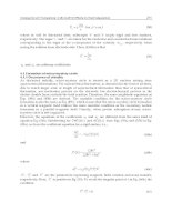
Schematic Fig. 9 illustrates the formation and evolution of the strain in a typical epitaxy film
growth process. At the film growth temperature, when atoms arrive at the surface of the
substrate, they will initially adopt the substrate’s in-plane lattice constant to form an
epitaxial film [Fig. 9(a)]. As long as the film thickness (t) is smaller than the critical thickness
(h
c
) of the film/substrate system, the film will keep its coherence with substrate and
maintain a fully strained layer [Fig. 9(b)]. When t > h
c
, dislocations will appear at the
interface or near interface region and the whole film relaxes. However, the relaxation is a
dynamic controlled process, if the film thickness is not large enough than h
c
, the relaxation
may only occur partially [Fig. 9(c)]. Finally, during the cooling process,
Fig. 9. An illustration of the strain formation and evolution in a typical epitaxy film growth
process.
additional thermal strain may also be exerted on film due to the difference of the TECs
between the film and substrate [Fig. 9(d)]. Therefore, the temperature dependent misfit
strain in a thin film can be modeled simply by taking into account the combined
Epitaxial Integration of Ferroelectric BaTiO
3
with Semiconductor Si:
From a Structure-Property Correlation Point of View
375
contribution of the temperature dependent lattice strain [S
m
(T
g
)] and the thermal strain
[S
therm
(T)] [59], which can be approximated by the linear relation,
() ( ) ()
mmgtherm
ST ST S T
(1)
() ( )( )
therm s f g
ST TT
(2)
where, T
g
= 873 K, is the growth temperature, S
therm
(T) is the thermal strain,
s
and
f
are
linear thermal expansion coefficients (TECs) of the substrate and prototypic cubic phase of
the film. S
m
(T
g
) = [a
s
*
(T
g
) – a
f
(T
g
)] / a
s
*
(T
g
) is the effective misfit strain of the film and
substrate at T
g
, a
s
*
= a
s
(1 -
) is the effective lattice parameter of the substrate [60] and
is
the dislocation density [61], which reflects the effect of strain relaxation induced by the
appearance of misfit dislocations at the film/substrate interface at T
g
.
For the convenience of understanding, we define an original misfit lattice strain S
m
0
(T
g
),
which means the actual original misfit strain between the as-grown film and the supporting
substrate if the film does not relax at all at the growth conditions, as follows,
0
()[() ()]/()
mg sg f g sg
S T aT aT aT
(3)
Taking into account the thermal expansion, the lattice constant of the film and substrate at
T
g
can be approximated by a
f
(T
g
) = a
f
(RT)[1 +
f
(T
g
- RT)] and a
s
(T
g
) = a
s
(RT)[1 +
s
(T
g
- RT)],
respectively. As a matter of fact, the S
m
0
(T
g
) does not really exist, because the film growth
and relaxation occur simultaneously. However, we assume the film growth process and the
strain relaxation process can occur in the following two successive steps. First, the film
doesn’t relax during the whole growth procedure (holding a S
m
0
(T
g
)) and then, when growth
is done the relaxation process dominates and the as-grown film begins to relax only when
the accumulated S
m
0
(T
g
) exceeds the critical relaxation requirements. In this picture, the S
m
(T
g
) in equation (1) can be thus equivalently and much more schematically divided into the
combination of an original lattice strain S
m
0
(T
g
) at T
g
and a strain variation due to the
formation of misfit dislocations [S
dis
(
, T
g
)] during relaxation,
0
() () (,)
mg mg dis g
ST ST S T
(4)
In addition, structural factors such as growth defects, crystallinity, and oxygen vacancies
may also contribute to the S
m
(T) [41], which is denoted by S
other
in the following expression.
0
() ( ) (, ) ()
mmgdisgthermother
ST ST S T S T S
(5)
By analyzing the first three terms on the right side of equation (5), we can roughly estimate
the final strain in the obtained film.
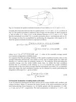
We start from the LNO buffer layer. Fig. 10 (a) shows the XRD patterns for various LNO
films with different thickness. It is obvious the LNO (200) peak shifts toward high angles
with increasing the film thicknesses, indicating a decrease in the lattice constant. Fig. 10 (b)
shows the LNO thickness dependent lattice constant (a = 2d
002
) and misfit strain (S
m
= (a –
a
0
)/a
0
, where a
0
is the lattice constant for freestanding bulk LNO) obtained from the XRD
result at RT. As can be seen, the lattice parameters decrease with increasing the LNO
thickness and become close to the bulk value (3.84 Å) for 600 nm LNO film.
Ferroelectrics – Material Aspects
376
Fig. 10. (a) XRD patterns for LNO films with different thicknesses. (b) Calculated LNO
thickness dependence of misfit strain and lattice constant, along with the lattice constant for
bulk LNO.
For the LNO film directly grown on a Si substrate, using equations (3), we can calculate the
origin misfit lattice strain and S
m
0
(T
g
) ~ -3.68×10
-3
. Based on elastic theory, the S
m
0
(T
g
) will
be fully relaxed by the formation of misfit dislocations at the film/substrate interface when
the thickness of the film (h) is larger enough than the critical thickness (h
c
) [62],
1
ln 1
4(1 )
c
c
h
b
h
fb
(6)
where
is the Poisson’s ratio, f the relative misfit, and b the Burger’s vector of misfit
dislocations. Due to lack of v value for LNO, here we simply assume
= 0.3, a typical value
for perovskite oxides [63], and h
c
is estimated to be on the order of 23 nm for a 0.5%-misfit
film. Considering that the film thickness t >> h
c
, so the S
m
0
(T
g
) will be fully relaxed by S
dis
(
,
T
g
), making S
m
0
(T
g
) and S
dis
(
, T
g
) negligible. The S
m
(T) in equation (5) is therefore
attributed mainly to the thermal strain S
therm
(T) and S
other
. Generally, due to large difference
in TECs between LNO and Si, the induced thermal strain will make the LNO film under a
tensile strain state with an enlarged lattice constant at room temperature, which is consistent
with the former XRD results. Using equation (2) the thermal strain S
therm
(T) at RT for the
LNO is estimated to be ~ 3.91 × 10
-3
, while the XRD analysis shows that S
m
(RT) for the LNO
films is decreased from 26.82 × 10
-3
to 2.865 × 10
-3
, as shown in the inset, when the thickness
varies from 50 nm to 600 nm. The result also indicates that a strain in the LNO films induced
by the Si substrate can be fully relaxed by increasing their thicknesses to a certain extent.
Note that the difference between S
m
(RT) values and the thermal strain also confirms the
contribution of structural parameters (S
other
), as represented in equation (5).
5.2 Tensile strained BTO
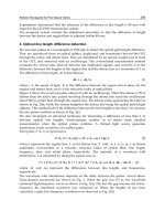
Fig. 11(a) shows the XRD patterns for 200 nm BTO films grown on the 100 nm LNO buffered
Si. In order to determine the in-plane lattice alignment and in-plane constant of BTO,
samples were placed on a tilted holder with a set azimuth angle of ψ = 45º, so that the (101)
and (202) crystal planes are parallel to the detected surface of the films. As a result, the
reflections for (101) and (202) planes in the film will become much easier to satisfy the
Epitaxial Integration of Ferroelectric BaTiO
3
with Semiconductor Si:
From a Structure-Property Correlation Point of View
377
Prague’s Law, 2dsinθ = λ (d is the lattice spacing, θ the diffraction angle and λ the x-ray wave
length) [64], in the x-ray detecting process and obvious diffraction of (101) and (202) planes
will occur at their own characteristic diffraction angle. The 45 º tilted XRD θ - 2θ scans for
BTO/LNO bi-layers are shown in Fig. 11(b). It is seen that only (101) and (202) reflections for
LNO and BTO films are detected, implying the in-plane lattice alignment between [110]
LNO and [110] BTO. Using lattice spacing d
002
and d
202
obtained from the Prague’s Law (d =
λ/2sinθ), the out-of-plane lattice constants (a
⊥
) and in-plane lattice constants (a
||
) for BTO
can be calculated by the following equations [65],
30 40 50 60 70
(b)
(202)
(202)
(101)
(101)
2Theta
(
de
g
.
)
Intensity (arb .units)
20 25 30 35 40 45 50
-20 0 -1 00 0 100 200
-30
-20
-10
0
10
20
30
Electric field (kV/cm)
Polarization (C/cm
2
)
Intensity (arb .units)
(001)
(001)
(002)
(002)
2 Theta
de
g
.
BaTiO
3
LaNiO
3
(a)
Fig. 11. (a) XRD patterns for 200 nm BTO thin film deposited on 100 nm LNO-buffered Si
substrate. Inset shows the room temperature ferroelectric hysteresis loop for this BTO film.
(b) 45º tilted in-plane scan for the BTO/LNO bilayer films.
002
2ad
(7)
||
22
202 002
2
11
a
dd
(8)
The obtained a
⊥
and a
||
for 200 nm BTO are 4.001 and 4.077 Å, respectively. Compared with
bulk BTO (a = 3.992 Å and c = 4.036 Å), the BTO films are elongated along a-axis and
compressed along c-axis. Besides, as out-of-plane lattice constants are always smaller than
the in-plane lattice constants for both BTO films, thus it can be inferred that the BTO films
are under an in-plane tensile strain state. Inset of Fig. 11(a) shows room temperature
polarization and capacitance with electric field at 1 kHz. The small remnant P
r
indicates that
the film is nearly in an in-plane polarization state, that is, the polarization vectors mainly
parallel to the film surface.
The temperature dependent dielectric permittivity and dielectric loss for the bilayer films
were shown in Fig. 12(a). Over the temperature region, two broad but obvious peaks for the
dielectric permittivity and dielectric loss are detected at 30 °C and 170 °C, respectively. This
indicates that two phase transitions have occurred. The dielectric response can be explained
Ferroelectrics – Material Aspects
378
by the misfit strain-temperature phase diagrams theory [66-71] for an epitaxial polydomain
ferroelectric film grown on a “tensile” substrate. As shown in Fig. 12(b), the polydomain
ferroelectric films have different phase states and domain configurations compared to
epitaxial single-domain film or bulk materials. This results in the contribution of an extrinsic
response (domain-wall movements) together with the intrinsic response (substrate induced
strain) to the dielectric response in a small signal dielectric measurement in the plate-
capacitor setup. The temperature dependent misfit strain can be approximated by equation
(1). Since BTO film is pretty thick, the contribution of lattice strain can be neglected, and the
total strain is subjected solely to the thermal strain. Thus, the misfit strain (S
m
) at the
ferroelectric phase transition temperature (443 K) is estimated to be (α
s
-α
f
)(T-T
g
) ~ 3.87 × 10
-
3
, which just lies in the predicated a
1
/a
2
/a
1
/a
2
polydomain region [66]. It can be obtained
that, when the film is cooled down from the deposition temperature to Curie temperature, a
second order phase transition from cubic parelectric to pseudo-tetragonal a
1
/a
2
/a
1
/a
2
ferroelectric phase occurs, leading to the appearance of the broad dielectric peak in the
temperature-dependent dielectric curves. On the other hand, the second permittivity peak at
30 °C
is suggested to be the result of the structural phase transition between the a
1
/a
2
/a
1
/a
2
and ca
1
/ca
2
/ca
1
/ca
2
polydomain states that is accompanied by the appearance of the out-of-
plane polarization. This is also consistent with the observation of the small P
r
at room
temperature.
-100 -50 0 50 100 150 200
260
280
300
320
340
360
-100 0 100 200
0.0
0.1
0.2
0.3
Temperature (°C)
Loss Tangent
Temperature (°C)
Dielectric Constant
1 kHz
2 kHz
3 kHz
10 kHz
100 kHz
1 MHz
Misfit strain S
m
(10
-3
)
T
e
m
p
e
r
a
t
u
r
e
(
°
C
)
-2 0 2 4 6
180
150
120
90
60
30
0
a
1
/a
2
/a
1
/a
2
polydomain
aa
1
/aa
2
/aa
1
/aa
2
polydomain
polydomain
a
1
/a
2
/a
1
/a
2
paraelectric
c-phase
(a) (b)
Fig. 12. (a) Temperature dependent dielectric permittivity and dielectric loss (inset) for the
tensile-strained BTO film. (b) Schematic illustration of the misfit strain-temperature for BTO
thin film.
Fig. 13(a) shows the plan-view HRTEM image of elastic domain pattern for the BTO film.
The adjacent elastic domain walls form a coherent twin boundary lying along the surface of
{110} twin planes for the minimization of in-plane elastic strain energy. Fig. 13(b) shows the
cross-sectional TEM image of elastic domains. It can be clearly seen that the domain walls
exhibit a blunt fringe contrast, because the polarization vectors in adjacent domains form an
angle
and they, as a result, are not in the same height with respect to the observation
direction [72].
Epitaxial Integration of Ferroelectric BaTiO
3
with Semiconductor Si:
From a Structure-Property Correlation Point of View
379
Fig. 13. (a) HRTEM plan-view image of elastic domain configurations, (b) cross-sectional
image of elastic domains.
5.3 Compressive strained BTO
Fig. 14(a) and 14(b) show the XRD patterns of normal and 45ºtilted θ-2θ scans of BTO(100
nm) on LNO(600 nm)/Si. Using above mentioned method, the in-plane and out-of-plane
lattice constants for the BTO film are calculated to be a = 3.955 Å and c = 4.056 Å,
respectively. Then the tetragonal distortion c/a is 1.025. Compared to bulk BTO (a = 3.992 Å
and c = 4.036 Å) and other tensile strained BTO films on Si substrates (e.g. c = 3.975 Å by
Meier et al. [40]), the BTO film is elongated along c-axis and compressed along a-axis, and
corresponds well with the results obtained by Petraru et al. in BTO (56 nm)/STO (a = 3.925 Å
and c = 4.125 Å) [73]. The unit cell volume can be estimated as V
film
= a × a × c ~ 63.444 Å
3
,
which is smaller than that of the bulk (V
teg
~ 64.318 Å
3
and V
cubic
~ 64.722 Å
3
) [74]. Therefore,
the BTO film is under a compressive strain state.
20 25 30 35 40 45 50
(001)
(002)
(002)
(001)
BaTiO
3
LaNiO
3
Intensity (arb.units)
2 Theta (deg.)
30 40 50 60 70
(202)
(202)
(101)
(101)
2 Theta (deg.)
Intensity (arb.units)
(a) (b)
Fig. 14. XRD patterns of regular (a) and 45
ºtilted (b) θ-2θ scans of
BTO(100nm)/LNO(600nm)/Si.
Ferroelectrics – Material Aspects
380
-6 -4 -2 0 2 4 6
-30
-20
-10
0
10
20
30
Polarization (C/cm
2
)
Electric field
(
V
)
-50 0 50 100 150 200
180
200
220
240
Dielectric constant
Tem
p
erature
(
°C
)
0.0
0.1
0.2
0.3
0.4
0.5
Loss tangent
L
o
s
s
t
a
n
g
e
n
t
(a)
(b)
Fig. 15. Room temperature hysteresis loop (a) and temperature dependent dielectric
response (b) for compressive strained BTO film.
Electrical properties of compressive strained BTO film have been investigated by
ferroelectric and dielectric measurements. Hysteresis loop for the compressive BTO, as
shown in Fig. 15(a), exhibits a well-defined shape, which is significantly different from
those of tensile BTO films. The P
r
is 10.2 µC/cm
2
, much larger than 0.7 µC/cm
2
and 2.0
µC/cm
2
observed in tensile BTO films on Si substrate [41,44], which is apparently due to
the compressive strain state induced by thick LNO layer. However, it should be noted
that the obtained P
r
is still smaller compared with the giant P
r
values for other fully
strained BTO films with purely c-domain structure on compressive oxide substrates, such
as SrTiO
3
[46], GdScO
3
and DyScO
3
[47]. Temperature dependent dielectric permittivity
and loss tangent curves exhibit a broad peak near 100 °C, showing a slight decrease in the
ferroelectric to parelectric phase transition temperature (T
c
) with respect to its bulk
counterparts [75]. The strain state dependent T
c
for BTO film had been extensively
investigated, and it is very dependent on the film or buffer layer thickness [76,77],
substrate chosen [78,79] as well as the microstructure and crystallinity [80,81] of the
fabricated BTO films. For example, Huang et al. [76] had fabricated BTO films with wide
range of thickness (35 ~ 1000 nm) on 400 nm LNO buffered Si substrates using Ar/O
2
mixed sputtering gas and found that all the films were tensile strained and the T
c
was
greatly reduced with decreasing the BTO film thickness. However, their BTO films were
significantly (110)-oriented instead of (001)-oriented. On the other hand, based on the
misfit strain-temperature phase diagrams theory for epitaxial polydomain ferroelectric
thin films, both tensile and compressive epitaxial strain will substantially enhance the T
c
for ideal homogeneous ferroelectric epitaxial films. However, it has recently been
demonstrated that in thin films the inhomogeneous strain field resulted by the strain
gradients in the growth direction of the film should also be considered, which, combined
with the homogeneous strain field, will both influence the polarization and ferroelectric
phase transition character of ferroelectric thin films [41,82,83]. In addition, Kato et al. [80]
observed a marked decrease of T
c
for 20 °C in polycrystalline BTO films on
LNO(200nm)/Pt(400nm)/Si and Chen et al. [81] also reported a reduced T
c
in
polycrystalline multiferroic NiFe/BTO/Si.
In fact, the reduction of T
c
for the ferroelectric crystals and films are commonly observed in
a system under an external compressive stress [74,81]. Based on the soft mode theory, the
phase transition for displacive ferroelectrics can be attributed to the frozen of soft mode in
Epitaxial Integration of Ferroelectric BaTiO
3
with Semiconductor Si:
From a Structure-Property Correlation Point of View
381
the center of Brillouin zone. The frequency of the soft mode (ω
T
) is determined by the
interaction between local restoring “short range” repulsions (R
0
'), which prefers the
undistorted paraelectric cubic structure, and “long range” Coulomb force, which stablizes
the ferroelectric distortions [84],
µω
T
2
= R
0
' - 4π(ε+2)(Z'e)
2
/9V (9)
where, µ is the reduced mass of the ions, Z'e the effective ionic charge, V the volume of the
unit cell, and ε the high frequency dielectric constant. The decreased lattice volume in the
compressive BTO film (V
film
< V
teg
< V
cubic
) leads to the decrease of average ion distance (r),
which in turn increases the short range force and the Coulomb force as well. Since the short
range force is proportional to r
–n
(n = 10~11) while the Coulomb force to r
-3
, the increase of
the former with decreasing r is much faster than the latter [85,86]. The result leads to the
stiffening of the soft mode, resulting in a lower ferroelectric transition temperature from a
macroscopic point of view.
Fig. 16. (a) Plan-view TEM image of domain configurations and (b) HRTEM image of elastic
domains for the compressive BTO film.
The compressive BTO exhibits very different domain configurations as compared with a
tensile BTO, in which twining a
1
/a
2
/a
1
/a
2
domain structure was observed. Fig. 16(a) shows
plan-view TEM image of domains for the compressive BTO film, in which lamellar domain
patterns are clearly observed. Further HRTEM observation, as shown in Fig. 16(b), reveals a
c/a/c/a domain pattern, in which c-domains have equal in-plane lattice parameters of a
1
=a
2
with polarization vectors parallel to c-axis and a-domains have non-equal in-plane lattice
parameters with polarization parallel to a-axis. These observations correspond well with the
typical c/a/c/a polydomain configurations in compressive ferroelectric films observed by
Lee et al. [72] and Alpay et al. [87].
5.4 Phase transition
Fig. 17(a) shows the normal XRD pattern for a 300 nm BTO thin film grown on the 600nm
LNO-buffered Si substrate. The lattice constants for BTO film are a = 3.982 and c = 4.053 Å,
thus it can be inferred that the sputtered BTO film is under an in-plane compressive strain
Ferroelectrics – Material Aspects
382
state. Fig. 17(b) and (c) demonstrate the HRTEM images of typical ferroelectric domains for
the BTO film. It is seen that a BTO grain is distinctively split by the appearance of laminar
domain configurations in order to minimize the in-plane elastic strain energy [88]. Similarly,
for this compressive strained BTO, the observed domain wall between adjacent domains
exhibits a blunt fringe contrast, indicating a c/a/c/a domain configuration.
Fig. 17. (a) XRD θ - 2θ scan for 300 nm BTO on LNO(600nm)/Si. Inset is the 45º tilted XRD θ -
2θ scan for the same film. (b) and (c) HRTEM lattice image of typical ferroelectric domains
inside a single BTO grain.
Fig. 18(a) and (b) show the temperature dependent dielectric constant (ε′) and dielectric loss
(tanδ) at different frequency of 1 - 500 kHz for the BTO film. It is observed that the Curie
temperature (T
c
), characterizing the ferroelectric to parelectric phase transition, is around
108 °C, which is lower than the value of typical T
c
for BTO bulk or single crystal. On the
other hand, in addition to the reduction of T
c
, several other feathers are also evidenced in
Fig. 18(a) and (b): (1) A broadened maximum in the dielectric constant appears at a wide
temperature ranging from 80 °C to 120 °C, (b) the magnitude of the dielectric constant
decreases, while T
c
increases with increasing frequency, (c) the peak in dielectric loss is also
frequency dependent and it shifts to higher temperatures with increasing frequency. The
above observed strongly frequency dependent dielectric properties resemble the typical
diffusive ferroelectric phase transition in ferroelectric relaxors rather than a normal
ferroelectric phase transition, which shows a sharp anomaly at the T
c
[89].
According to Smolensky and Uchino et al. [90,91], the diffuseness of the phase transition can
be investigated by a modified Curie-Weiss (CW) law,
1/ε′-1/ε′
m
= (T-T
m
)
γ
/C (10)
where ε′ is the dielectric constant at temperature T, ε′
m
is the dielectric constant at T
m
, γ is the
critical exponent, and C is the Curie constant. A value of γ = 1 indicates a normal transition
with ideal CW behavior, whereas γ = 2 indicates a diffusive transition behavior. The plot of
log(1/ε′-1/ε′
m
) as a function of log(T-T
m
) at 1 kHz is shown in the Fig. 19(a). By fitting the
Epitaxial Integration of Ferroelectric BaTiO
3
with Semiconductor Si:
From a Structure-Property Correlation Point of View
383
modified CW law, the exponent γ, determining the degree of the diffuseness of the phase
transition, can be extracted from the slope of log(1/ε′-1/ε′
m
) - log(T-T
m
) plot. The relatively
high γ value of 1.624 also indicates a relaxor behavior, which seems to be inconsistent with
the predominant concept that BTO is a typical displacive ferroelectric material and should
exhibit sharp dielectric transition [92].
0 50 100 150 200
360
390
420
450
Tem
p
erature
(
°C
)
1 kHz
2 kHz
3 kHz
5 kHz
10 kHz
20 kHz
50 kHz
100 kHz
200 kHz
500 kHz
0 50 100 150 200
0.1
0.2
0.3
0.4
Temperature (°C)
tan
(a) (b)
Fig. 18. Temperature dependent (a) dielectric constant and (b) loss tangent for the BTO film
at frequency range of 1 kHz ~ 500 kHz.
Fig. 19. (a) log(1/ε′-1/ε′
m
) - log(T-T
m
) plot for the BTO film at 1 kHz. (b) ln(f) – 1/(T
m
-T
vf
) plot
for the BTO film at 1 kHz. Symbol represents experimental data and solid dot line shows the
fitting result.
However, recent nuclear magnetic resonance and Raman scattering studies had both
evidenced the coexistence of the displacive character of transverse optical soft mode with
the order-disorder character of Ti ions [93], especially in the BTO thin films. As the
sputtering is proceed in an oxygen deficient atmosphere, thus the oxygen vacancies induced
structural disorders and compositional fluctuations in the film may be responsible for the
observed relaxor behavior. Similar diffusive transition had also been observed in BTO films
on MgO and Pt-coated Si substrates [94,95].
Ferroelectrics – Material Aspects
384
The relaxor nature of the frequency dependent dielectric response of BTO film can also be
examined by the Vogel-Fulcher (VF) relation [96],
f = f
0
exp[-E
a
/k(T
m
-T
vf
)] (11)
where f is the measuring frequency, f
0
is the characteristic relaxation frequency, E
a
is the
activation energy, T
m
is the phase transition temperature at f, and T
vf
is the freezing
temperature of polarization-fluctuation. The ln(f) – 1/(T
m
-T
vf
) plot with best fittings for the
film is displayed in Fig. 19(b). The validity of VF relationship further demonstrates the
relaxor behavior. From the slop of the fittings, the corresponding parameters can be
obtained, f
0
~ 3.12108 Hz, T
vf
~ 327.3 K and E
a
~ 0.097 eV.
6. Conclusions
High quality ferroelectric BTO thin films with (100)-preferred orientation have been grown
on LNO buffered Si substrate by rf sputtering and the corresponding structure-property
correlations have been discussed. Using combination of XRD and HRTEM, it is revealed that
highly-oriented BTO film could be achieved on the lattice-mismatched Si in a “cube-on-
cube” fashion with LNO as both buffer layer and conductive electrode layer. Polarization-
switching measurement points out that while obvious ferroelectricity is obtained for BTO
films with grain size larger than 22 nm, a weak ferroelectricity is still observed in BTO film
of 14 nm grains, indicating that if a critical grain size exists for ferroelectricity it is less than
14 nm for BTO/LNO/Si system. We also demonstrate that due to their unique feature of
gradient lattice constant and thermal expansion coefficient values for ferroelectric BTO,
conductive LNO, and substrate Si, the BTO/LNO/Si system exhibits very interesting strain
states. By choosing appropriate thicknesses for BTO and LNO, strain in ferroelectric BTO
layer could be evolved from tensile strain to compressive strain state. The internal strain has
a significant influence on the polarization, dielectric phase transition, and domain
configuration for BTO film on Si and this can be used as a tool to engineer the properties of
BTO films. The present work may have important implications on the future ferroelectric
semiconductor devices.
7. Acknowledgements
This work is supported by the innovation Foundation of BUAA for PhD Graduates and
program for New Century Excellent Talents in university (NCET-04-0160) and Innovative
Research Team in University (IRT0512).
8. References
[1] Y. Yano, K. Iijima, Y. Daitoh, a T. Terashim, Y. Bando, Y. Watanabe, H. Kasatani and H.
Terauchi, J. Appl. Phys. 76, 7833 (1994).
[2] S. Kim and S. Hishita, Thin Solid Films 281-282, 449 (1996).
[3] L. Qiao and X. F. Bi, Thin Solid Films 517, 3784 (2009).
[4] R. E. Avila, J. V. Caballero, V. M. Fuenzalida and I. Eisele, Thin Solid Films 348 44 (1999).
[5] T. Pencheva and M. Nenkov, Vacuum 48, 43 (1997).
[6] D. Y. Kim, S. G. Lee, Y. K. Park and S. J. Park, Mater. Lett. 40, 146 (1999).
Epitaxial Integration of Ferroelectric BaTiO
3
with Semiconductor Si:
From a Structure-Property Correlation Point of View
385
[7] X. H. Wei, Y. R. Li, J. Zhu, Z. Liang, Y. Zhang, W. Huang and S. W. Jiang, Appl. Surf. Sci.
252, 1442 (2005).
[8] T. W. Kim, M. Jung, Y. S. Yoon, W. N. Kang, H. S. Shin, S. S. Yom and J. Y. Lee, 1993 Solid
State Commun. 86, 565 (1993).
[9] K. Yao and W. G. Zhu, Thin Solid Films 408, 11 (2002).
[10] W. Xu, L. Zheng, H. Xin, C. Lin and O. Masanori, J. Electrochem. Soc. 143, 1133 (1996).
[11] S. A. Chambers, Adv. Mater. 22, 219 (2010).
[12] J. W. Reiner, A. M. Kolpak, Y. Segal, K. F. Garrity, S. I. Beigi, C. A. Ahn, and F. J. Walker,
Adv. Mater. 22, 2929 (2010).
[13] M. P. Warusawithana, C. Cen, C. R. Sleasman, J. C. Woicik, Y. L. Li, L. F. Kourkoutis, J.
A. Klug, H. Li, P. Ryan, L. P. Wang, M. Bedzyk, D. A. Muller, L. Q. Chen, J. Levy,
and D. G. Schlom, Science 324, 367 (2009).
[14] J. Schwarzkopf and R. Fornari, Prog. Crystal Growth Character. Mater. 52, 159 (2006).
[15] A. K. Tagantsev, N. A. Pertsev, P. Muralt, and N. Setter, Phys. Rev. B 65, 012104 (2001).
[16] W. Y. Park, K. H. Ahn, and C. S. Hwanga. Appl. Phys. Lett. 83, 4387 (2003).
[17] S. B. Mi, C. L. Jia, T. Heeg, O. Trithaveesak, J. Schubert, and K. Urban, J. Cryst. Growth
283, 425 (2005).
[18] O. Auciello, J. F. Scott, and R. Ramesh, Phys. Today 51(7), 22 1998).
[19] J. Levy, Phys. Rev. A 64, 052306 (2001).
[20] V. Vaithyanathan, J. Lettieri, W. Tian, A. Sharan, A. Vasudevarao, Y. L. Li, A. Kochhar,
H. Ma, J. Levy, P. Zschack, J. C. Woicik, L. Q. Chen, V. Gopalan, and D. G. Schlom,
J. Appl. Phys. 100, 024108 (2006).
[21] Y. S. Touloukian, R. K. Kirby, R. E. Taylor, and T. Y. R. Lee, Thermal Expansion,
Nonmetallic Solids, Thermophysical Properties of Matter (Plenum, New York,
1977), Vol. 13.
[22] L. Qiao and X. F. Bi, J. Cryst. Growth 310, 5327 (2008).
[23] L. W. Martin, Y. H. Chu, R. Ramesh, Mater. Sci. Eng. Rep. 68, 111 (2010).
[24] A. B. Posadas, M. Lippmaa, F. J. Walker, M. Dawber, C. H. Ahn, and J. M. Triscone,
Topics. Appl. Phys. 105, 219 (2007).
[25] E. Kawamura, V. Vahedi, M. A. Lieberman, and C. K. Birdsall, Plasma Sources Sci Technol
R45, 240 (1999).
[26] B. G. Chae, Y. S. Yang, S. H. Lee, M. S. Jang, S. J. Lee, S. H. Kim, W. S. Baek, S. C. Kwon,
Thin Solid Films 410, 107 (2002).
[27] N. Wakiya, T. Azuma, K. Shinozaki, N. Mizutani, Thin Solid Films 410, 114
(2002).
[28] D. H. Bao, N. Mizutani, X. Yao and L. Y. Zhang, Appl. Phys. Lett. 77, 1041 (2000).
[29] Q. Zou, H. E. Ruda and B. G. Yacobi, Appl. Phys. Lett. 78, 1282 (2001).
[30] D. H. Bao, N. Wakiya, K. Shinozaki, N. Mizutani and X. Yao, Appl. Phys. Lett. 78, 3286
(2001).
[31] J. R. Cheng, L. He, S. W. Yu and Z. Y. Meng, Appl. Phys. Lett. 88, 152906 (2006).
[32] S. Schlag and H. F. Eicke, Solid State Commun. 91, 883 (1994).
[33] W. Zhong, B. Jiang, P. Zhang, J. Ma, H. Chen, Z. Yang and L. Li, J. Phys.: Condens. Matter
5, 2619 (1993).
[34] S. Chattopanhuay, P. Ayyub, V. R. Palkar and M. Multani, Phys. Rev. B 52, 13177 (1995).
Ferroelectrics – Material Aspects
386
[35] S. Li, J. A. Eastman, J. M. Vetrone, C. M. Foster, R. E. Newnham and L. E. Cross, Jpn. J.
Appl. Phys., Part I 36, 5169 (1997).
[36] T. Maruyama, M. Saitoh, I. Sakay and T. Hidaka, Appl. Phys. Lett. 73, 3524 (1998).
[37] Y. S. Kim, D. H. Kim, J. D. Kim, Y. J. Chang, T. W. Noh, J. H. Kong, K. Char, Y. D. Park,
S. D. Bu, J G. Yoon and J S. Chung, Appl. Phys. Lett. 86, 102907 (2005).
[38] J. Junquera and P. Ghosez, Nature 422, 506 (2003).
[39] D. D. Fong, G. B. Stephenson, S. K. Streiffer, J. A. Eastman, O. Auciello, P. H. Fuoss and
C. Thompson, Science 304, 1650 (2004).
[40] A. R. Meier, F. Niu and B. W. Wessels, J. Crystal Growth, 294, 401 (2006).
[41] B. Dkhil, E. Defay and J. Guillan, Appl. Phys. Lett. 90, 022908 (2007).
[42] H. Huang, X. Yao, M. Q. Wang and X. Q. Wu, J. Crystal Growth 263, 406 (2004).
[43] Y. P. Guo, K. Suzuki, K. Nishizawa, T. Miki and K. Kato, J. Crystal Growth 284, 190
(2005).
[44] R. Thomas, V. K. Varadan, S. Komarneni and D. C. Dube, J. Appl. Phys. 90, 1480 (2001).
[45] L. M. Huang, Z. Y. Chen, J. D. Wilson, S. Banerjee, R. D. Robinson, I. P. Herman, R.
Laibowitz and S. O’Brien, J. Appl. Phys. 100, 034316 (2006).
[46] Y. S. Kim, J. Y. Jo, D. J. Kim, Y. J. Chang, J. H. Lee, T. W. Noh, T. K. Song, J G. Yoon, J S.
Chung, S. I. Baik, Y W. Kim and C. U. Jung, Appl. Phys. Lett. 88, 072909 (2006).
[47] K. J. Choi, M. Biegalski, Y. L. Li, A. Sharan, J. Schubert, R. Uecker, P. Reiche, Y. B. Chen,
X. Q. Pan, V. Gopalan, L. Q. Chen, D. G. Schlom and C. B. Eom, Science 306, 1005
(2004).
[48] M. T. Buscaglia, M. Viviani, V. Buscaglia, L. Mitoseriu, A. Testino, P. Nanni, Z. Zhao, M.
Nygren, C. Harnagea, D. Piazza andi C. Galass, Phys. Rev. B. 73, 064114 (2006).
[49] X. Y. Deng, X. H. Wang, H. Wen, L. L. Chen, L. Chen and L. T. Li, Appl. Phys. Lett. 88,
252905 (2006).
[50] X. H. Wang, X. Y. Deng, H. Wen and L. T. Li, Appl. Phys. Lett. 89, 162902 (2006).
[51] G. Liu, X. H. Wang, Y. Lin, L. T. Li and C. W. Nan, J. Appl. Phys. 98, 044105 (2005).
[52] Y. Park and H-G. Kim, J. Am. Ceram. Soc. 80(1), 106 (1997).
[53] T. Takeuchi, M. Tabuchi, H. Kageyama and Y. Suyama, J. Am. Ceram. Soc. 82(4), 939
(1999).
[54] G. Arlt, D. Hennings and G. de With, J. Appl. Phys. 58, 1619 (1985).
[55] J. H. Haenl, P. Irvin, W. Chang, R. Uecker, P. Reiche, Y. L. Li, S. Choudhury, W. Tian, M.
E. Hawley, B. craigo, A. K. Tagantsev, X. Q. Pan, S. K. Streiffer, L. Q. Chen, S. W.
Kirchoefer, J. Levy, and D. G. Schlom, Nature 430, 758 (2004).
[56] J. Q. He, E. Vasco, R. Dittmann, and R. H. Wang, Phys. Rev. B 73, 125413 (2006).
[57] H. D. Kang, W. H. Song, S. H. Sohn, H. J. Jin, S. E. Lee, and Y. K. Chung, Appl. Phys. Lett.
88, 172905 (2006).
[58] M. Jimi, T. Ohnishi, K. Terai, M. Kawasaki, M. Lippmaa, Thin Solid Films 486, 158 (2005).
[59] N. A. Pertsev, A. G. Zembilgotov, S. Hoffmann, R. Waser, and A. K. Tagantsev, J. Appl.
Phys. 85, 1698 (1999).
[60] K. S. Lee and S. Baik, J. Appl. Phys. 87, 8035 (2000).
[61] R. Dittmann, R. Plonka, E. Vasco, N. A. Pertsev, J. Q. He, C. L. Jia, S. Hoffmann, and R.
Waser, Appl. Phys. Lett. 83, 5011 (2003).
[62] R. People and J. C. Bean, Appl. Phys. Lett. 47, 322 (1985).
Epitaxial Integration of Ferroelectric BaTiO
3
with Semiconductor Si:
From a Structure-Property Correlation Point of View
387
[63] J. M. Gere and S. P. Timoshenko, Mechanics of Materials, 4th ed. (PWS, Boston, 1997), p.
889.
[64] M. S. Rafique and N. Tahir, Vacuum 81, 1062 (2007).
[65] D. Y. Wang, Y. Wang, X. Y. Zhou, H. L. W. Chan and C. L. Choy, Appl. Phys. Lett. 86,
212904 (2005).
[66] N. A. Pertsev, V. G. Koukhar, R. Waser, and S. Hoffmann, Integrated Ferroelectrics 32, 235
(2001)
[67] N. A. Pertsev, A. G. Zembilgotov and A. K. Tagantsev, Phys. Rev. Lett. 80, 1988
(1998).
[68] N. A. Pertsev, A. G. Zembilgotov and A. K. Tagantsev, Ferroelectrics 223, 79 (1999).
[69] N. A. Pertsev and V. G. Koukhar, Phys. Rev. Lett. 84, 3722 (2000).
[70] V. G. Koukhar, N. A. Pertsev, and R. Waser, Phys. Rev. B 64, 214103 (2001).
[71] Y. L. Li and L. Q. Chen, Appl. Phys. Lett. 88, 072905 (2006).
[72] K. S. Lee, J. H. Choi, J. Y. Lee, and S. Baik, J. Appl. Phys. 90, 4095 (2001).
[73] A. Petraru, N. A. Pertsev, H. Kohlstedt, U. Poppe, R. Waser, A. Solbach, and U.
Klemradt, J. Appl. Phys. 101, 114106 (2007).
[74] Z. H. Dai, Z. Xu, and X. Yao, Appl. Phys. Lett. 92, 072904 (2008).
[75] D. A. Tenne, X. X. Xi, Y. L. Li, L. Q. Chen, A. Soukiassian, M. H. Zhu, A. R.
James, J. Lettieri, D. G. Schlom, W. Tian and X. Q. Pan, Phys. Rev. B 69,
174101 (2004)
[76] G. F. Huang and S. Berger, J. Appl. Phys. 93, 2855 (2003).
[77] L. Qiao and X. F. Bi, J. Phys. D: Appl. Phys. 41, 195407 (2008).
[78] K. M. Ring and K. L. Kavanagh, J. Appl. Phys. 94, 5982 (2003).
[79] M. E. Marssi, F. L. Marrec, I. A. Lukyanchuk and M. G. Karkut, J. Appl. Phys. 94, 3307
(2003).
[80] K. Kato, K. Tanaka, K. Suzuki and S. Kayukawa, Appl. Phys. Lett. 91, 172907 (2007).
[81] Y. C. Chen, T. H. Hong, Z. X. Jiang and Q. R. Lin, J. Appl. Phys. 103, 07E305 (2008).
[82] G. Catalan, B. Noheda, J. McAneney, L. J. Sinnamon, and J. M. Gregg, Phys. Rev. B 72,
020102R (2005).
[83] G. Catalan, L. J. Sinnamon, and J. M. Gregg, J. Phys.: Condens. Matter 16, 2253
(2004).
[84] W. Cochran, Phys. Rev. Lett. 3, 412 (1959).
[85] G. A. Samara, T. Sakudo, and K. Yoshimitsu, Phys. Rev. Lett. 35, 1767 (1975)
[86] R. E. Cohen, Nature 358, 136 (1992).
[87] S. P. Alpay, V. Nagarajan, L. A. Bendersky, M. D. Vaudin, S. Aggarwal, R. Ramesh, and
A. L. Roytburd, J. Appl. Phys. 85, 3271 (1999).
[88] I. T. Kim, J. W. Jang, H. J. Youn, C. H. Kim and K. S. Hong, Appl. Phys. Lett. 72, 308
(1998).
[89] B. D. Qu, M. Evstigneev, D. J. Johnson and R. H. Prince, Appl. Phys. Lett. 72, 1394 (1998).
[90] G. A. Smolensky, J. Phys. Soc. Jpn. 28, 26 (1970).
[91] K. Uchino and S. Nomura, Ferroelectr. Lett. Sect. 44, 55 (1982).
[92] M. M. Kumar, K. Srinivas and S. V. Suryanarayana, Appl. Phys. Lett. 76, 1330 (2000).
[93] M. Tyunina and J. Levoska, Phys. Rev. B 70, 132105 (2004).
Ferroelectrics – Material Aspects
388
[94] S. Chattopadhyay, A. R. Teren, J. H. Hwang, T. O. Mason and B. W. Wessels, J. Mater.
Res. 17, 669 (2002).
[95] R. Thimas, V. K. Varadan, S. Komarneni and D. C. Dube, J. Appl. Phys. 90, 1480
(2001).
[96] J. Xu and Y. Akishige, Appl. Phys. Lett. 92, 052902 (2008).
19
Nanostructured LiTaO
3
and KNbO
3
Ferroelectric Transparent Glass-Ceramics
for Applications in Optoelectronics
Anal Tarafder and Basudeb Karmakar
Glass Science and Technology Section, Glass Division,
Central Glass and Ceramic Research Institute,
Council of Scientific and Industrial Research (CSIR, India),
India
1. Introduction
Ferroelectric bulk crystals are widely used in optoelectronic devices because of their well
combination of extraordinary optical and electronic properties. Their crystal structure is
non-centrosymmetric and due to this structural anisotropy they exhibit many nonlinear
optical properties, for example, the electro-optic effect (change in optical index with electric
field), harmonic generation (changing frequency of light), and photorefraction (index
change in response to light), to name a few. However, preparation of their defect-free optical
quality transparent single crystal is very difficult, lengthy process, and requires
sophisticated costly equipment. In recent past, to triumph over these difficulties, much
attention has been paid for development of transparent ferroelectric glass-ceramics by the
high speed glass technology route because of its low cost of fabrication, tailoring of
properties and flexibility to give desired shapes. Lithium tantalate (LiTaO
3
, LT) and
potassium niobate (KNbO
3
, KN) single crystals are the most important lead-free ferroelectric
materials with the A
1+
B
5+
O
3
type perovskite structure concerning the environmental
friendliness. LT has the rhombohedral crystal structure with crystal symmetry class 3m (unit
cell dimensions: a = 5.1530 Å and c = 13.755 Å), large nonlinear constant (d
33
= 13.6 pm/V at
1064 nm), second harmonic generation (SHG) coefficient (
2
33
w
d = 40.0 with respect to KDP at
1060 nm) (Risk et al., 2003, JCPDS No. 29-0836, Moses, 1978) and Curie temperature (660°C).
In contrast, KN has the orthorhombic crystal structure with crystal symmetry class mm2
(unit cell dimensions: a = 5.6896 Å, b = 3.9693 Å and c = 5.7256 Å), large nonlinear coefficient
(d
33
= 27.4 pm/V at 1064 nm) [Moses, 1978] and Curie temperature (435°C). Thus, they
exhibit unique electro-optic, piezoelectric, acousto-optic, and nonlinear optical (NLO)
properties when doped with rare-earth (RE) [4f
1-13
] elements combined with good
mechanical and chemical stability (Abedin et al., 1997, Zhu et al., 1995, Mizuuchi et al., 1995,
Zgonik et al., 1993, Xue et al., 1998). Very recently, potassium niobate ceramics were
investigated with an aim to develop environmental friendly lead-free piezoelectric and
nonlinear materials (Ringgaard & Wurlitzer, 2005).
The electronic structure of each trivalent RE element consists of partially filled 4f subshell,
and outer 5s
2
and 5p
6
subshell. With increasing nuclear charge electrons enter into the
underlying 4f subshell rather than the external 5d subshell. Since the filled 5s
2
and 5p
6
Ferroelectrics – Material Aspects
390
subshells screen the 4f electrons, the RE elements have very similar chemical properties. The
screening of the partially filled 4f subshells, by the outer closed 5s
2
and 5p
6
subshell, also
gives rise to sharp emission spectra independent of the host materials. The intra-subshell
transitions of 4f electrons lead to narrow absorption peaks in the ultra-violet, visible, and
near-infrared regions.
In this chapter, we report synthesis, structure, properties and application of transparent
ferroelectric LiTaO
3
(LT) and KNbO
3
(KN) nanostructured glass-ceramics. They were
prepared by controlled volume (bulk) crystallization of their precursor glasses with and
without RE dopant. The crystallization processes were studied by differential thermal
analysis (DTA), X-ray diffraction (XRD), field emission scanning electron microscopy
(FESEM), transmission electron microscopy (TEM), Fourier transform infrared reflection
spectra (FT-IRRS), fluorescence and excited state lifetime analyses and dielectric constant
measurement. The X-ray diffraction (XRD) patterns, selected area electron diffraction
(SAED) and transmission electron microscopic (TEM) images confirm crystallization of
LiTaO
3
and KNbO
3
nanocrystals in the transparent glass-ceramics.
2. Experimental procedure
2.1 Precursor glass and glass-ceramics preparation
The LT precursor glasses having molar composition 25.53Li
2
O-21.53Ta
2
O
5
-35.29SiO
2
-
17.65Al
2
O
3
(LTSA) doped with RE ions (0.5 wt% oxides of Eu
3+
and Nd
3+
in excess) or
undoped were prepared by the melt-quench technique. The melting of thoroughly-mixed
batches was done at 1600°C. The quenched glass blocks were annealed at 600°C for 4 h to
remove the internal stresses of the glass and then slowly cooled down (@ 1°C/min) to room
temperature. The annealed glass blocks were cut into desired dimensions and optically
polished for ceramization and to perform different measurements. The crystallization was
carried out at 680°C in between 0-100 h duration.
The KN precursor glasses having composition (mol%) 25K
2
O-25Nb
2
O
5
-50SiO
2
(KNS) doped
with Er
2
O
3
(0.5 wt% in excess) or undoped were prepared similarly as mentioned above by
the melt-quench technique. The well-mixed raw materials were melted in a platinum
crucible in an electric furnace at 1550°C and the quenched glasses were annealed at 600°C to
remove the internal stresses of these precursor glasses. They were transformed into
nanostructured transparent glass-ceramics by heat-treatment at 800°C in between 0-200 h
duration.
2.2 Characterization
The density of precursor glasses was measured using Archimedes principle using water as
buoyancy liquid. The refractive indices of precursor glass and representative glass-ceramics
(d) were measured either on a Pulfrich refractometer (Model PR2, CARL ZEISS, Jena,
Germany) at wavelength (λ
e
= 546.1 nm) or on a Metricon 2010/M Prism Coupler at
different wavelength (λ
= 473, 532, 633, 1064 and 1552 nm). Differential thermal analysis
(DTA) of precursor glass powder was carried out up to 1000°C at the rate of 10°C/min with
a SETARAM TG/DTA 92 or with a Netzsch STA 409 C/CD instrument from room
temperature to 900°C at a heating rate of 10°C/min. to ascertain the glass transition
temperature (T
g
) and the crystallization peak temperature (T
P
). XRD data were recorded
Nanostructured LiTaO
3
and KNbO
3
Ferroelectric
Transparent Glass-Ceramics for Applications in Optoelectronics
391
using a PANalytical X’Pert-PRO MPD diffractometer operating with CuK
α
= 1.5406 Å
radiation to identify the developed crystalline phases. The data were collected in the 2θ
range from 10° to 80° with a step size of 0.05°.
A high resolution FE-SEM (Model: Gemini Zeiss Supra
TM
35 VP, Carl Zeiss) was used to
observe the microstructure of freshly fractured surfaces of the heat-treated nano glass-
ceramics after etching in 1% HF solution for 2 minutes and coated with a thin carbon film.
The TEM images and selected area electron diffraction (SAED) of powdered glass-ceramic
sample were obtained from FEI (Model: Tecnai G
2
30ST, FEI Company) instrument. The
FTIR reflectance spectra of all the glasses and glass-ceramics were recorded using a FTIR
spectrometer (Model: 1615, Perkin-Elmer) in the wavenumber range 400-2000 cm
-1
with a
spectral resolution of ±2 cm
-1
and at 15° angle of incidence. Optical absorption spectra were
recorded on UV-Vis-NIR spectrophotometer (Model: Lambda 20, Perkin-Elmer) at room
temperature. The UV-Vis fluorescence emission and excitation spectra of Eu
3+
doped
precursor glass and nano glass-ceramics were measured on a fluorimeter (Model:Fluorolog-
II, SPEX) with 150 W Xe lamp as a source of excitation. The fluorescence decay curves were
recorded on the same instrument attached with SPEX 1934D phosphorimeter using pulsed
Xe lamp. On the other hand, the fluorescence emission and excitation spectra of rest of
samples were measured on continuous bench top modular spectrofluorimeter
(QuantaMaster, Photon Technology International) attached with gated Hamamatsu NIR
PMT (P1.7R) as detector and Xe arc lamp as excitation source. The excited state lifetime was
measured with the same instrument using a Xe flash lamp of 75 W. The dielectric constants
of precursor glass and nano glass-ceramics were measured at room temperature using a
Hioki LCR meter (Model: 3532-50 Hitester, Hioki) at 1 MHz frequency after coating the
surfaces with a conductive silver paint followed by drying at 140°C for 1h. Second harmonic
generations (SHG) at 532 nm in the undoped glass-ceramics have been realized under
fundamental beam of Nd
3+
:YAG laser source (1064 nm). The input energy of Nd
3+
: YAG
laser was fixed at 17 mJ. The input energy of laser was divided in two directions (50%
energy in each direction) using reflecting neutral density filter. In one direction KDP was
put for reference. The reference SHG signal was measured using photodiode. Second beam
was passed through visible filter (which blocks all visible wavelengths but pass 1064 nm)
and focused onto the test samples. The SHG generated from the sample was focused onto a
second harmonic separator, which reflects 532 nm at 45° and transmit 1064 nm. The SHG
signal reflected from SHG separator passed through IR filter was finally measured using
PMT. The reference signals from photodiode and from PMT were measured simultaneously
using Lecroy oscilloscope (bandwidth 1GHz).
3. Nanostructured LiTaO
3
ferroelectric glass-ceramics
3.1 Background
Lithium tantalate (LiTaO
3
, LT) single crystal is one of the most important lead-free
ferroelectric materials in the A
1+
B
5+
O
3
type perovskite family. The correlation of property
alteration of LT single crystals, powders, thin films, glass-ceramics, etc. with processing
parameters is an important area of exploration. In recent times researchers have
demonstrated the property monitoring based on preparation of LiTaO
3
powders (Zheng et
al., 2009) and thin films (Cheng et al., 2005, Youssef et al., 2008) by different methods.
Luminescence properties of Ho
3+
, Eu
3+
, Tb
3+
etc. doped LiTaO
3
crystals, an another
important area of exploration, which have also been investigated by various researchers
(Sokólska, 2002, Sokólska et al., 2001, Gasparotto et al., 2008, Gruber et. al., 2006). Rare-earth
(RE) doped transparent LiTaO
3
nanocrystallite containing glass ceramics, in which RE ions
Ferroelectrics – Material Aspects
392
selectively incorporated into the LiTaO
3
nanocrystals embedded in an oxide glassy matrix,
can offer excellent luminescent properties due to the low phonon energy environment of
LiTaO
3
nanocrystallites for luminescent ions, and good mechanical and chemical properties
of oxide glassy matrix. This ability, combined with inherent nonlinear optical (NLO)
properties of ferroelectric crystals, could offer a possibility to design self frequency doubling
laser sources. Hence, this new material has attracted great attention in the continuous
research for the development of novel optoelectronic devices (Jain, 2004, Romanowski et al.,
2000, Hase et al., 1996). Mukherjee and Varma have reported the crystallization and physical
properties of LiTaO
3
in a LiBO
2
-Ta
2
O
5
reactive glass matrix, however, they have not
explored RE doped LiTaO
3
containing glass-ceramics (Mukherjee & Varma, 2004). As such,
work performed on nanocrystalline LiTaO
3
containing aluminosilicate glass-matrix
materials is very rare due to the difficulties in preparation of transparent precursor glass in
general and glass–ceramics in particular which involves high temperature (about 1600°C)
for its precursor glass melting (Ito et al., 1978). For this reason, the structure, dielectric and
fluorescence properties of Eu
3+
, Nd
3+
and Er
3+
ion doped transparent precursor glass and
glass-ceramic composites of LiTaO
3
with heat-treatment time have been studied and
reported elaborately by Tarafder et al., 2009 & 2010, Tarafder et al., DOI:10.1111/j.1744-
7402.2010.02494.x. Second harmonic generation (SHG) from bulk LiTaO
3
glass-ceramics has
also been studied (Tarafder et al., 2011). For better understanding, the structure, dielectric
and fluorescence properties of Eu
3+
and Nd
3+
ion doped transparent precursor glass and
glass-ceramic composites of LiTaO
3
with heat-treatment time have been reported elaborately
along with the second harmonic generation (SHG) from bulk LiTaO
3
glass-ceramics.
4. Results and discussion
4.1 Differential thermal analysis (DTA)
The DTA curve of the Eu
3+
doped precursor glass is shown in Fig. 1. This exhibits the
inflection in the temperature range 680-715°C followed by the intense exothermic peak at
821°C (T
p
) corresponding to the LiTaO
3
crystallization. The glass transition temperature (T
g
)
has been estimated to be 696°C from the point of intersection of the tangents drawn at the
slope change as is marked in Fig. 1.
600 650 700 750 800 850 900
0
20
40
60
80
100
→
→
→
→
Endo.
T
p
= 821
o
C
T
g
= 696
o
C
Exo.
Temperature (°C)
Fig. 1. DTA curve of Eu
3+
doped precursor LTSA powdered glass.
Nanostructured LiTaO
3
and KNbO
3
Ferroelectric
Transparent Glass-Ceramics for Applications in Optoelectronics
393
4.2 Refractive index
The Eu
3+
doped precursor LTSA glass samples were heat treated at 680°C near glass
transition temperature for various heat-treatment durations (0, 1, 3, 5, 7, and 10 h) after
nucleating at 650°C for 2 h. Similarly, the Nd
3+
doped precursor LTSA glass samples were
heat treated at 680°C for 0, 3, 5, 10, 20, 50 and 100 h and were labeled as a, b, c, d, e, f and g.
The Nd
3+
doped precursor glass and nano glass-ceramics are presented in Fig. 2. From the
measured glass density (ρ) and refractive index (n
e
) at wavelength λ
e
= 546.1 nm, other
related optical properties of Eu
3+
doped precursor glass have been determined using
relevant expressions and the same is presented in Table 1. Fig. 3 present Cauchy fitting
based on measured refractive indices at five different wavelengths (see experimental
procedure) and shows the dependences of the refractive index on the wavelength for Nd
3+
doped precursor glass (a) and representative heat-treated glass-ceramics samples. In
general, refractive index decreases with increasing wavelength due to dispersion. In
addition to this, the refractive index of the glass-ceramics samples has increased in
comparison with precursor glass (a) that can be seen in Fig. 3. The refractive indices n
F
, n
D
and n
C
have been estimated at three standard wavelengths (λ
F
= 486.1 nm, λ
D
= 589.2 nm
and λ
C
= 656.3 nm respectively) from the dispersion curve (Figs. 3, curve a). Similarly, from
the measured glass density (ρ) and refractive index (n
D
) at wavelength λ
D
= 589.2 nm, other
related optical properties of Nd
3+
doped precursor glass have also been determined and the
results are presented in Table 1. From Table 1, it is clear that the LTSA glass under study has
high values of refractive index and density. The large refractive indices of this glass are due
to high ionic refraction (23.4)
of Ta
5+
ions (Volf, 1984)
having an empty or unfilled d-orbital
(outer electronic configuration: 5d
0
6s
0
) which contributes strongly to the linear and
nonlinear polarizability (Yamane & Asahara, 2000). The high density of the glass has
originated from the large packing effect of Ta in the glass matrix (Hirayama & Berg, 1963).
For the same reason, this glass possesses a high value of molar refractivity and electronic
polarizability. Due to formation of high refractive index LiTaO
3
(RI = 2.1834 at 600 nm
(Lynch, 1975)), the heat-treated sample exhibit higher refractive indices as shown in Fig. 3,
curve-d.
Fig. 2. (Color online) Photographs of Nd
3+
doped precursor LTSA glass and LT nano glass-
ceramics (thickness: 2 mm) laid over the writing to show their transparency respectively.
4.3 X-ray diffraction analysis
The X-ray diffractogram of Eu
3+
doped precursor LTSA glass and cerammed glass-ceramics
are shown in Fig. 4. The XRD pattern of the precursor glass exhibits broad humps
characterizing its amorphous structure. With progression of heat-treatment, several
diffraction peaks have been appeared in the glass-ceramics. From the analysis of these peaks
it has been concluded that these peaks are attributed to rhombohedral LiTaO
3
(JCPDS Card
Ferroelectrics – Material Aspects
394
Properties
Corresponding value
Eu
3+
:LiTaO
3
doped
precursor glass
Nd
3+
:LiTaO
3
doped
precursor glass
Average molecular weight,
M
av
142.47 142.37
Density, ρ (g.cm
-3
) 4.54 4.50
Refractive index n
e
(at 546.1 nm) 1.7852
n
F
(at 486.1 nm) 1.8053
n
D
(at 589.2 nm) 1.7894
n
C
(at 656.3 nm) 1.7821
Molar refractivity, R
M
(cm
3
) 13.23 13.39
Electronic polarizability, α
(cm
3
)
1.84×10
-21
1.79 x 10
-21
RE
3+
ion concentration, N
RE
3+
(ions/cm
3
)
5.71×10
19
5.66 x 10
19
Glass transition temperature,
T
g
(°C)
696 702
Crystallization peak, T
p
(°C) 821 820
Table 1. Some measured and calculated properties of RE
3+
:LiTaO
3
precursor glass
Fig. 3. Variation of refractive indices (Cauchy fitted) of Nd
3+
doped (a) precursor LTSA glass
and (d) 10 h heat-treated LT nano glass-ceramic as a function of wavelength.
File No. 29-0836) except a few diffraction peak around 2θ = 23.0°, 25.5°, 44.5° and 47.0°
which are due to the formation of β-spodumene (LiAlSi
2
O
6
) crystal phase (JCPDS Card File
No. 35-0797) in minor quantity. It is clearly evidenced from the XRD analysis that the peak
of LiAlSi
2
O
6
(2θ = 25.5°) is more prominent in sample of 5 h heat-treatment and it got
diminished with respect to LiTaO
3
phase in longer heat-treated glass-ceramics, indicating
the stabilization of LiTaO
3
nanocrystallites with increase in heat-treatment duration. From
the full width at half maximum (FWHM) of the most intense diffraction peak (012) of
Nanostructured LiTaO
3
and KNbO
3
Ferroelectric
Transparent Glass-Ceramics for Applications in Optoelectronics
395
LiTaO
3
, the average crystallite size (diameter, d) is calculated by using the Scherrer’s
formula (Cullity, 1978)
0.9 / cosd
λ
β
θ
= (1)
where λ is the wavelength of X-ray radiation (CuK
α
= 1.5406Å), β is the full width at half
maximum (FWHM) of the peak at 2θ. The average crystallite size of each RE doped heat-
treated glass-ceramics found to increase with heat-treatment duration.
10 20 30 40 50 60 70 80
→
Spodumene
LiTaO
3
( JCPDS Card File 29-0836 )
128
312
306
220
1010
208
300
214
018
122
116
024
202
113
006
110
104
012
f
d
c
a
Intensity (a.u.)
2θ (degree)
Fig. 4. XRD pattern of Eu
3+
doped precursor powdered LTSA glass and LT nano glass-
ceramics.
4.4 FESEM and TEM image analyses
The morphology and LiTaO
3
crystallite size of Eu
3+
and Nd
3+
doped nano glass-ceramics
have been examined by FESEM and TEM image analyses. FESEM images of the fractured
surface of Nd
3+
doped nano glass-ceramics have been presented in Figs. 5(a)-(b). The Nd
3+
doped glass-ceramics 5(a) is obtained by heat-treating the precursor glasses at 680°C for 5 h.
Similarly, the glass-ceramics 5(b) is obtained by heat-treating the precursor glasses at 680°C
for 20 h. From the FESEM micrographs, it is clearly observed that the glassy matrix of the
heat-treated samples initially phase separated on nanometric scale followed by incipient
precipitation of defined crystallites within the Li–Ta rich phase regions with increase in
heat-treatment time. The droplets have irregular shapes and dispersed uniformly thought
out the bulk glass matrix. The size of the droplets varies in the range 20-60 nm. TEM image
of the Eu
3+
doped 10 h heat-treated glass-ceramics (f) has been presented in Fig. 6(a). The
SAED pattern of the observed crystalline phase is presented in Fig. 6(b). From this image, it
is observed that many spheroidal LiTaO
3
crystallites precipitated homogeneously from the
glass matrix and remained homogeneously dispersed in the residual glass matrix. The
crystallite size from this TEM image of sample f found to be around 18 nm. The presence of
fine spherical rings around the central bright region in SAED pattern discloses the existence
of LiTaO
3
nanocrystallites in the glassy matrix.
Ferroelectrics – Material Aspects
396
Fig. 5. FESEM image of Nd
3+
doped samples (a) c and (b) e.
Fig. 6. (a) TEM image and (b) SAED pattern of Eu
3+
doped glass-ceramics sample f.
4.5 Fourier transform infrared reflectance spectroscopy (FTIRRS)
The FTIR reflectance spectra of the Nd
3+
doped precursor LTSA glass and heat-treated glass-
ceramic samples in the wavenumber range 400-2000 cm
-1
is shown in Fig. 7. It is seen from
this figure that the precursor glass (curve-a) exhibits two broad reflection bands centered
around 960 and 610 cm
-1
as a result of wider distribution of silicon and tantalate structural
units respectively. As alumina is one of the glass constituents, it prefers to enter into the
silica rich phase and somewhere replace the Si
4+
and the charge is compensated by Li
+
ion.
But, in order to maintain neutral charge condition, the later phase contains a higher amount
of Li
+
ions as the TaO
6
octahedra are negatively charged (Fukumi & Sakka, 1988, Samuneva
et al., 1991). Hence, from the rearrangement of the glassy matrix it can be indicated that both
the phase separated compositions begin to crystallize producing a nanostructure with the
prolonged heat-treatment time. The appearance of a low intensity band at 735 cm
-1
upon
heat-treatment related to the stretching mode of Al-O bond of AlO
4
tetrahedra of β-
spodumene (Burdick & Day, 1967).
The prominent band occurred at 600 cm
-1
corresponds to
the stretching mode of O-Ta bond of TaO
6
octahedral units of lithium tantalate (Ono et al.,
2001, Zhang et al., 1999). The reflection band centered at 600 cm
-1
is assigned as LiTaO
3
crystal formation and the reflection band centered at 1000 cm
-1
is assigned to Si-O stretching
50 nm
(a)
(b)
(a)
(b)
100 nm
100 nm
Nanostructured LiTaO
3
and KNbO
3
Ferroelectric
Transparent Glass-Ceramics for Applications in Optoelectronics
397
vibration of residual glass and β-spodumene crystal. The variation of Si-O (998 cm
-1
) and Ta-
O (602 cm
-1
) stretching vibration bands intensities (here reflectivity) of Nd
3+
doped samples
with heat-treatment time is also recorded. It is seen that with progression of heat-treatment
the band intensities increase rapidly initially and then become almost saturated after a
certain time of heat-treatment (10 h). The gradual increase of relative intensity of band at 600
cm
-1
clearly indicates formation of LiTaO
3
crystal with the increase of heat treatment time.
The results of the FT-IRRS are in good agreement with that of XRD, FE-SEM and TEM
studies. A similar observation has also been reported by Ito et al., 1978.
Fig. 7. FTIR-RS spectra of Nd
3+
doped precursor LTSA glass and LT nano glass-ceramics.
4.6 Dielectric constant (ε
r
)
The as prepared Eu
3+
and Nd
3+
doped LTSA precursor glasses exhibit relatively higher
value (~20.0) of dielectric constant (
ε
r
) than the common vitreous silica (3.8) or soda-lime
silicate (7.2) or borosilicate glasses (4.1-4.9) (Blech, 1986) due to high ionic refraction of Ta
5+
ions (23.4) (Volf, 1984). This is due to its empty or unfilled d-orbital which contributes very
strongly to its high polarizability (Yamane & Asahara, 2000, Risk et al., 2003). Its magnitudes
show a sharp increase with increase in heat-treatment duration up to 5 h and thereafter it
maintained saturation with a small decrease for any further heat treatment time as shown in
Fig. 8. This suggests that, at the initial stages of heat treatment (1-3 h), separation of silica
rich phase and Li–Ta enriched phases takes place and with the further heat-treatment,
incipient precipitation of LiTaO
3
crystalline phase of high dielectric constant (ε
r
= 52) (Moses,
1978) and spontaneous polarization (P
s
= 0.50 C/m
2
) (Risk et al., 2003) occurs gradually
which becomes well defined at 5 h and attains the maximum volume fraction of the
crystalline phase. Thus accumulation of Li
+
ions in the phase-separated glass matrix initially
could cause a slight increase of dielectric constant and with further heat treatment time due
to formation of stable LiTaO
3
ferroelectric crystals remarkably increase the dielectric
constant reaching the highest value for 5 h heat treated sample and then maintain almost
same on further course of heat-treatment. The variation in the dielectric constant (
ε
r
) values
among the heat-treated nano glass-ceramics are mostly due to volume fraction of crystal
Ferroelectrics – Material Aspects
398
phases contained and also the distribution of the LiTaO
3
phase in the microstructure
(Vernacotola, 1994).
-10 0 10 20 30 40 50 60 70 80 90 100 110
18
20
22
24
26
28
30
32
Dielectric Constant (ε
r
)
Heat-Treatment Time (h)
Fig. 8. Variation of dielectric constant of Nd
3+
doped precursor LTSA glass and LT nano
glass-ceramics as a function of heat-treatment time.
4.7 UV-Visible-NIR absorption spectra
The room temperature measured absorption spectra of the Nd
3+
doped precursor glass (a)
and 100 h heat-treated glass-ceramic samples (g) in the visible-NIR range have been
presented in Fig. 9. The spectra reveal absorption peaks due to the 4f
3
-4f
3
forced electric
dipole transitions from the ground
4
I
9/2
state to different excited states of Nd
3+
ion in 4f
3
configuration. All the peaks
4
I
9/2
→
4
G
9/2
(512 nm),
2
K
13/2
+
4
G
7/2
+
4
G
9/2
(526 nm),
4
G
5/2
+
2
G
7/2
(583 nm),
2
H
11/2
(626 nm),
4
F
9/2
(679 nm),
4
F
7/2
+
4
S
3/2
(739 nm),
4
F
5/2
+
2
H
9/2
(806 nm) and
4
F
3/2
500 550 600 650 700 750 800 850 900
0.00
0.15
0.30
0.45
0.60
0.75
→
→
→
→
→
→
→
→
4
F
3/2
4
F
5/2
+
2
H
9/2
4
F
7/2
+
4
S
3/2
4
F
9/2
2
H
11/2
4
G
5/2
+
2
G
7/2
2
K
13/2
+
4
G
7/2
+
4
G
9/2
4
G
9/2
g
a
Relative Absorbane
(absorbance unit)
Wavelength (nm)
Fig. 9. Absorption spectra of Nd
3+
doped samples (a) and (g) (thickness: 2 mm).