Flash Memories Part 5 potx
Bạn đang xem bản rút gọn của tài liệu. Xem và tải ngay bản đầy đủ của tài liệu tại đây (1.23 MB, 20 trang )
Error Correction Codes and Signal Processing in Flash Memory
69
Here r is the received codeword and H is defined as the parity matrix
Each element of GF(2
m
)
i
can be represented by a m-tuples binary vector, hence each
element in the vector can be obtained using mod-2 addition operation, and all the
syndromes can be obtained with the XOR-tree circuit structure. Furthermore, for binary
BCH codes in flash memory, even-indexed syndromes equal the squares of the other one,
i.e., S
2i
=S
i
2
,
therefore, only odd-indexed syndromes (S
1
, S
3
…S
2t-1
) are needed to compute.
Then we propose a fast and adaptive decoding algorithm for error location. A direct solving
method based on the Peterson equation is designed to calculate the coefficients of the error-
location polynomial. Peterson equation is show as follows
11
223 11
21211
2
. . .
. . .
. . . . .
. . . . .
. .
ttt
ttt
tttt
SSSS
SSSS
SSSS
(18)
For DEC BCH code t=2, with the even-indexed syndrome S
1,
S
3
, the coefficient
1
,
2
can be
obtained by direct solving the above matrix as
2
1121 31
, /SSSS
(19)
Hence, the error-locator polynomial is given by
222
3
12 1 1
1
11() ( )
S
xxxSxSx
S
(20)
To eliminate the complicate division operation in above equation, a division-free
transform is performed by multiplying both sides by S
1
and the new polynomial is
rewritten as (21). Since it always has S
1
0 when any error exists in the codeword, this
transform has no influence of error location in Chien search where roots are found in (x)
=0, that is also ’(x) =0.
2232
01 2 11 13
''''
() ( )xxxSSxSSx
(21)
The final effort to reduce complexity is to transform the multiplications in the coefficients of
equation (21) to simple modulo-2 operations. As mentioned above, over the field GF(2
m
),
each syndrome vector (S[0], S[1],
. . .
S[m-1]) has a corresponding polynomial S(x) = S[0]
+
S[1]x+
. . .
+ S[m-1]x
m-1
. According to the closure axiom over GF(2
m
), each component of the
coefficient
1
and
2
is obtained as
11
23 11
01
01
'
'
[] [] for ,
[] [] [] [ ] for , ,
iSj ijm
iSi SjSk ijkm
(22)
It can be seen that only modulo-2 additions and modulo-2 multiplications are needed to
calculate above equation, which can be realized by XOR and AND logic operations,
respectively. Hardware implementation of the two coefficients in BCH(274, 256, 2) code is
Flash Memories
70
shown in Fig. 12. It can be seen that coefficient
1
is implemented with only six 2-input XOR
gates and coefficient
2
can be realized by regular XOR-tree circuit structure. As a result, the
direct solving method is very effective to simplify the decoding algorithm, thereby reduce
the decoding latency significantly.
Fig. 12. Implementation of the two coefficient in BCH(274,256,2)
Further, an adaptive decoding architecture is proposed with the reliability feature of flash
memory. As mentioned above, flash memory reliability is decreased as memory is used. For
the worst case of multi-bit errors in flash memory, 1-bit error is more likely happened in the
whole life of flash memory (R. Micheloni, R. Ravasio & A. Marelli, 2006). Therefore, the best-
effort is to design a self-adaptive DEC BCH decoding which is able to dynamically perform
error correction according to the number of errors. Average decoding latency and power
consumption can be reduced.
The first step to perform self-adaptive decoding is to detect the weight-of-error pattern in
the codeword, which can be obtained with Massey syndrome matrix.
1
321
21 2 2 21
1 0 0
0
j
jj j j
S
LSSS
SS S S
(23)
where S
j
denotes each syndrome value (1≤j≤2t-1).
With this syndrome matrix, the weight-of-error pattern can be bounded by the expression of
det(L
1
), det(L
2
), …, det(L
t
). For a DEC BCH code in NOR flash memory, the weight-of-error
pattern is illustrated as follows
If there is no error, then det(L1) = 0, det(L2) = 0, that is,
1
3
13
00, SSS
(24)
If there are 1-bit errors, then det(L
1
)≠0, det(L
2
) = 0, that is
1
3
13
00, SSS
(25)
If there are 2-bit errors, then det(L
1
)≠0, det(L
2
)≠0, that is
1
3
13
00, SSS
(26)
Error Correction Codes and Signal Processing in Flash Memory
71
Let define R= S
1
3
+ S
3
. It is obvious that variable R determines the number of errors in the
codeword. On the basis of this observation, the Chien search expression partition is
presented in the following:
Chien search expression for SEC
1
2
1
() ()
ii
SEC
SS
for 2
m
- n ≤ i ≤2
m
–1
(27)
Chien search expression for DEC
2
() () ()
iii
DEC SEC
R
for 2
m
- n ≤ i ≤2
m
–1
(28)
Though above equations are mathematically equivalent to original expression in equation
(21), this reformulation make the Chien search for SEC able to be launched once the
syndrome S
1
is calculated. Therefore, a short-path implementation is achieved for SEC
decoding in a DEC BCH code. In addition, expression (27) is included in expression (28),
hence, no extra arithmetic operation is required for the faster SEC decoding within the DEC
BCH decoding. Since variable R indicates the number of errors, it is served as the internal
selection signal of SEC decoding or DEC decoding. As a result, self-adaptive decoding is
achieved with above proposed BCH decoding algorithm reformulation.
To meet the decoding latency requirement, bit-parallel Chien search has to be adopted. Bit-
parallel Chien search performs all the substitutions of (28) of n elements in a parallel way,
and each substitution has m sub-elements over GF(2
m
). Obviously, this will increase the
complexity drasmatically. For BCH(274, 256, 2) code, the Chien search module has 2466
expression, each can be implemented with a XOR-tree. In (X. Wang, D. Wu & C. Hu, 2009),
an optimization method based on common subexpression elimination (CSE) is employed to
optimize and reduce the logic complexity.
4.2 High-speed BCH decoder implementation
Based on the proposed algorithm, a high-speed self-adaptive DEC BCH decoder is design
and its architecture is depicted in Fig. 13. Once the input codeword is received from NOR
flash memory array, the two syndromes S
1
, S
3
are firstly obtained by 18 parallel XOR-trees.
Then, the proposed fast-decoding algorithm is employed to calculate the coefficients of error
location polynomial in the R calculator module. Meanwhile, a short-path is implemented for
SEC decoding once the syndrome value S
1
is obtained. Finally, variable R determines
whether SEC decoding or DEC decoding should be performed and selects the according
data path at the output.
Fig. 13. Block diagram of the proposed DEC BCH decoder.
The performance of an embedded BCH (274,256,2) decoder in NOR flash memory is
summarized in Table 2. The decoder is synthesized with Design Compiler and implemented
in 180nm CMOS process. It has 2-bit error correction capability and achieves decoding
Flash Memories
72
latency of 4.60ns. In addition, it can be seen that the self-adaptive decoding is very effective
to speed up the decoding and reduce the power consumption for 1-bit error correction. The
DEC BCH decoder satisfies the short latency and high reliability requirement of NOR flash
memory.
Code Parameter BCH(274, 256) codes
Information data 256 bits
Parity bits 18 bits
Syndrome time 1.66ns
Data output time
1-bit error 3.53ns
2-bit errors 4.60ns
Power consumption
(Vdd=1.8V, T=70ns)
1-bit error 0.51mW
2-bit error 1.25mW
Cell area 0.251 mm2
Table 2. Performance of a high-speed and self-adaptive DEC BCH decoder
5. LDPC ECC in NAND flash memory
As raw BER in NAND flash increases to close to 10
-2
at its life end, hard-decision ECC, such
as BCH code, is not sufficient any more, and such more powerful soft-decision ECC as
LDPC code becomes necessary. The outstanding performance of LDPC code is based on
soft-decision information.
5.1 Soft-decision log-likelihood information from NAND flash
Denote the sensed threshold voltage of a cell as V
th
, the distribution of erase state as ,
the distribution of programmed states as
, where is the index of
programmed state. Denote
as the set of the states whose -th bit is 0. Thus, given the ,
the LLR of i-th code bit in one cell is:
(29)
Clearly, LLR calculation demands the knowledge of the probability density functions of all
the states, and threshold voltage of concerned cells.
There exist many kinds of noises, such as cell-to-cell interference, random-telegraph noise,
retention process and so on, therefore it would be unfeasible to derive the closed-form
distribution of each state, given the NAND flash channel model that captures all those noise
sources. We can rely on Monte Carlo simulation with random input to get the distribution of
all states after being interrupted by several noise sources in NAND flash channel. With
random data to be programmed into NAND flash cells, we run a large amount of simulation
on the NAND flash channel model to get the distribution of all states, and the obtained
threshold voltage distribution would be very close to real distribution under a large amount
of simulation. In practice, the distribution of
can be obtained through fine-grained
sensing on large amount of blocks.
Error Correction Codes and Signal Processing in Flash Memory
73
In sensing flash cell, a number of reference voltages are serially applied to the
corresponding control gate to see if the sensed cell conduct, thus the sensing result is not the
exact target threshold voltage but a range which covers the concerned threshold voltage.
Denote the sensed range as
( and are two adjacent reference voltages). There
is be
.
Example 2: Let’s consider a 2-bit-per-cell flash cell with threshold voltage of 1.3V. Suppose
the reference voltage starts from 0V, with incremental step of 0.3V. The reference voltages
applied to the flash cell is: 0, 0.3V, 0.6V, 0.9V, 1.2V, 1.5V This cell will not be open until the
reference voltage of 1.5V is applied, so the sensing result is that the threshold voltage of this
cell stays among (1.2, 1.5].
The corresponding LLR of i-th bit in one cell is then calculated as
(30)
5.2 Performance of LDPC code in NAND flash
With the NAND flash model presented in section 2 and the same parameters as those in
Example 1, the performances of (34520, 32794, 107) BCH code and (34520, 32794) QC-LDPC
codes with column weight 4 are presented in Fig. 14, where floating point sensing is
assumed on NAND flash cells. The performance advantage of LDPC code is obvious.
0 2000 4000 6000 8000 10000
10
-3
10
-2
10
-1
10
0
Cycling
PER
LDPC
BCH
Fig. 14. Page error rate performances of LDPC and BCH codes with the same coding rate
under various program/erase cycling.
5.3 Non-uniform sensing in NAND flash for soft-decision information
As mentioned above, sensing flash cell is performed through applying different reference
voltages to check if the cell can open, so the sensing latency directly depends on the number of
applied sensing levels. To provide soft-decision information, considerable amount of sensing
levels are necessary, thus the sensing latency is very high compared to hard-decision sensing.
Flash Memories
74
Soft-decision sensing increases not only the sensing latency, but also the data transfer latency
from page buffer to flash controller, since these data is transferred in serial.
Example 3: Let’s consider a 2-bit-per-cell flash cell with threshold voltage of 1.3V. Suppose
the hard reference voltages as 0, 0.6V and 1.2V respectively. Suppose sensing one reference
voltage takes 8us. The page size is 2K bytes and I/O bus works as 100M Hz with 8-bit
width. For hard-decision sensing, we need to apply all three hard reference voltages to sense
it out, resulting in sensing latency of 24us. To sense a page for soft-decision information
with 5-bit precision, we need
us, more than ten times the hard-decision sensing
latency. With 5-bit soft-decision information per cell, the total amount of data is increased by
2.5 times, thus the data transfer latency is increased by 2.5 times, from 20.48 us to
51.2us. The overall sensing and transfer latency jumps to 51.2+256=307.2 us from
20.48+24=44.48 us.
Based on above discussion, it is highly desirable to reduce the amount of soft-decision
sensing levels for the implementation of soft-decision ECC. Conventional design practice
tends to simply use a uniform fine-grained soft-decision memory sensing strategy as
illustrated in Fig. 15, where soft-decision reference voltages are uniformly distributed
between two adjacent hard-decision reference voltages.
Fig. 15. Illustration of the straightforward uniform soft-decision memory sensing. Note that
soft-decision reference voltages are uniformly distributed between any two adjacent hard-
decision reference voltages.
Intuitively, since most overlap between two adjacent states occurs around the corresponding
hard-decision reference voltage (i.e., the boundary of two adjacent states) as illustrated in
Fig. 15, it should be desirable to sense such region with a higher precision and leave the
remainder region with less sensing precision or even no sensing. This is a non-uniform or
non-linear memory sensing strategy, through which the same amount of sensing voltages is
expected to provide more information.
Given a sensed threshold voltage V
th
, its entropy can be obtained as
(31)
Where
Error Correction Codes and Signal Processing in Flash Memory
75
(32)
For one given programmed flash memory cell, there are always just one or two items being
dominating among all the
items for the calculation of . Outside of the
dominating overlap region, there is only one dominating item very close to 1 while all the
other items being almost 0, so the entropy will be very small. On the other hand, within the
dominating overlap region, there are two relatively dominating items among all the
items, and both of them are close to 0.5 if locates close to the hard-
decision reference voltage, i.e., the boundary of two adjacent states, which will result in a
relatively large entropy value
. Clearly the region with large entropy tends to demand a
higher sensing precision. So, it is intuitive to apply a non-uniform memory sensing strategy as
illustrated in Fig. 16. Associated with each hard-decision reference voltage at the boundary of
two adjacent states, a so-called dominating overlap region is defined and uniform memory
sensing is executed only within each dominating overlap region.
Given the sensed
of a memory cell, the value of entropy is mainly determined by
two largest probability items, and this translates into the ratio between the two largest
probability items. Therefore, such a design trade-off can be adjusted by a probability ratio
, i.e., let denote the dominating overlap region between two adjacent states, we
can determine the border
and by solving
(33)
Fig. 16 Illustration of the proposed non-uniform sensing strategy. Dominating overlap
region is around hard-decision reference voltage, and all the sensing reference voltages only
distribute within those dominating overlap regions.
Since each dominating overlap region contains one hard-decision reference voltage and two
borders, at least
sensing levels should be used in non-uniform sensing. Simulation
results on BER performance of rate-19/20 (34520, 32794) LDPC codes in uniform and non-
uniform sensing under various cell-to-cell interference strengths for 2 bits/cell NAND flash
are presented in Fig. 17. Note that at least 9 non-uniform sensing levels is required for non-
uniform sensing for 2 bits/cell flash. The probability ratio
is set as 512. Observe that
Flash Memories
76
Fig. 17. Performance of LDPC code when using the non-uniform and uniform sensing
schemes with various sensing level configurations.
15-level non-uniform sensing provides almost the same performance as 31-level uniform
sensing, corresponding to about 50% sensing latency reduction. 9-level non-uniform sensing
performs very closely to 15-level uniform sensing, corresponding to about 40% sensing
latency reduction.
6. Signal processing for NAND flash memory
As discussed above, as technology continues to scale down and hence adjacent cells become
closer, parasitic coupling capacitance between adjacent cells continues to increase and results
in increasingly severe cell-to-cell interference. Some study has clearly identified cell-to-cell
interference as the major challenge for future NAND flash memory scaling. So it is of
paramount importance to develop techniques that can either minimize or tolerate cell-to-cell
interference. Lots of prior work has been focusing on how to minimize cell-to-cell interference
through device/circuit techniques such as word-line and/or bit-line shielding. This section
presents to employ signal processing techniques to tolerate cell-to-cell interference.
According to the formation of cell-to-cell interference, it is essentially the same as inter-
symbol interference encountered in many communication channels. This directly enables
the feasibility of applying the basic concepts of post-compensation, a well known signal
processing techniques being widely used to handle inter-symbol interference in
communication channel, to tolerate cell-to-cell interference.
6.1 Technique I: Post-compensation
It is clear that, if we know the threshold voltage shift of interfering cells, we can estimate the
corresponding cell-to-cell interference strength and subsequently subtract it from the sensed
threshold voltage of victim cells. Let
denote the sensed threshold voltage of the -th
interfering cell and
denote the mean of erased state, we can estimate the threshold
voltage shift
of each interfering cell as . Let denote the mean of the
corresponding coupling ratio, we can estimate the strength of cell-to-cell interference as
Error Correction Codes and Signal Processing in Flash Memory
77
(34)
Therefore, we can post-compensate cell-to-cell interference by subtracting estimated
from
the sensed threshold voltage of victim cells. In [Dong, Li & Zhang, 2010], the authors presents
simulation result of post-compensation on one initial NAND flash channel with the odd/even
structure. Fig. 18 shows the threshold voltage distribution before and after post-compensation.
It’s obvious that post-compensation technique can effectively cancel interference.
Note that the sensing quantization precision directly determines the trade-off between the cell-
to-cell interference compensation effectiveness and induced overhead. Fig. 19 and Fig. 20 show
the simulated BER vs. cell-to-cell coupling strength factor
for even and odd pages, where 32-
level and 16-level uniform sensing quantization schemes are considered. Simulation results
clearly show the impact of sensing precision on the BER performance. Under 32-level sensing,
post-compensation could provide large BER performance improvement, while 16-level sensing
degrades the odd cells’ performance when cell-to-cell interference strength is low.
Fig. 18. Simulated victim cell threshold voltage distribution before and after post-
compensation.
Reverse Programming for Reading Consecutive Pages
To execute post-compensation for concerned page, we need the threshold voltage
information of its interfering page. When consecutive pages are to be read, information on
the interfering pages become inherently available, hence we can capture the approximate
threshold voltage shift and estimate the corresponding cell-to-cell interference on the fly
during the read operations for compensation.
Since sensing operation takes considerable latency, it would be feasible to run ECC
decoding on the concerned page first, and sensing the interfering page will not be started
until that ECC decoding fails, or will be started while ECC decoding is running.
Flash Memories
78
Fig. 19. Simulated BER performance of even cells when post-compensation is used.
Fig. 20. Simulated BER performance of odd cells when post-compensation is used.
Note that pages are generally programmed and read both in the same order, i.e. page with
lower index is programmed and read prior to page with higher index in consecutive case.
Since later programmed page imposes interference on previously programmed neighbor
page, as a result, one victim page is read before its interfering page is read in reading
consecutive pages, hence extra read latency is needed to wait for reading interfering page of
each concerned page. In the case of consecutive pages reading, all consecutive pages are
concerned pages, and each page acts as the interfering page to the previous page and
meanwhile is the victim page of the next page. Intuitively, reversing the order of
programming pages to be descending order, i.e., pages with lower index are programmed
latter, meanwhile reading pages in the ascending order can eliminate this extra read latency
in reading consecutive pages. This is named as reverse programming scheme.
In this case, when we read those consecutive pages, after one page is read, it can naturally
serve to compensate cell-to-cell interference for the page being read later. Therefore the extra
sensing latency on waiting for sensing interfering page is naturally eliminated. Note that this
reverse programming does not influence the sensing latency of reading individual pages.
Error Correction Codes and Signal Processing in Flash Memory
79
6.2 Technique II: Pre-distortion
Pre-distortion or pre-coding technique widely used in communication system can also be
used in NAND flash: Before a page is programmed, if its interfering pages are also known,
we can predict the threshold voltage shift induced by cell-to-cell interference for each victim
cell, and then correspondingly pre-distort the victim cell target programming voltage.
Hence, after its interfering pages are programmed, the pre-distorted victim cell threshold
voltages is expected to shift to its desired location by cell-to-cell interference.
Let
denote the expected threshold voltage of the
-th interfering cell after programming
and
denote the mean of erased state, we can predict the cell-to-cell interference
experienced by the victim cell as
(35)
Let
denote the target verify voltage of the victim cell in programming operation, we can
pre-distort the victim cell by shifting the verify voltage from
to . The threshold
voltage of the victim cell will be shifted towards its desired location after the occurrence of cell-
to-cell interference. It should be emphasized that, since we cannot change the threshold
voltage if the victim cell should stay at the erased state, this pre-distortion scheme can only
handle cell-to-cell interference for those programmed states but is not effective for erased state.
Fig. 21 illustrates the process of pre-distortion, where the verify voltage
is assumed to be
able to be adjusted with a floating-point precision. Clearly, this technique can be considered
as a counterpart of the post-compensation technique.
Fig. 21. Illustration of threshold voltage distribution of victim even cells in even/odd
structure when data pre-distortion is being used.
Fig.22 shows the cell threshold distribution with the cell-to-cell interference strength factor
under the same initial NAND flash channel model as in above subsection, where
the pre-distortion is assumed to be able to be adjusted with a floating-point precision.
Fig. 23 shows the simulated BER of even cells over a range of cell-to-cell interference
strength factor s. Besides the ideal floating point precision, pre-distortion with finite
precision is also shown, where the range of pre-distorted
is quantized into either 16 or 32
Flash Memories
80
levels. Clearly, as the finite quantization precision of pre-distorted increases, it can
achieve a better tolerance to cell-to-cell interference, at the cost of increased programming
latency, a larger page buffer to hold the data and higher chip-to-chip communication load.
Fig. 22. Simulated threshold voltage distribution when using pre-distortion.
Fig. 23. The simulated BER of even cells with pre-distortion under various cell-to-cell
strength factor.
7. Reference
K. Kim et.al, “Future memory technology: Challenges and opportunities,” in Proc. of International
Symposium on VLSI Technology, Systems and Applications, Apr. 2008, pp. 5–9.
Error Correction Codes and Signal Processing in Flash Memory
81
G. Dong, S. Li, and T. Zhang, “Using Data Post-compensation and Pre-distortion to Tolerat
Cell-to-Cell Interference in MLC NAND Flash Memory”, IEEE Transactions on
Circuits and Systems I, vol. 57, issue 10, pp. 2718-2728, 2010
Y. Li and Y. Fong, “Compensating for coupling based on sensing a neighbor using
coupling,” United States Patent 7,522,454, Apr. 2009.
G. Dong, N. Xie, and T. Zhang, “On the Use of Soft-Decision Error Correction Codes in
NAND Flash Memory”, IEEE Transactions on Circuits and Systems I, vol. 58, issue 2,
pp. 429-439, 2011
E. Gal and S. Toledo, “Algorithms and data structures for flash memories,” ACM Computing
Surveys, vol. 37, pp. 138–163, June 2005.
Y. Pan, G. Dong, and T. Zhang, “Exploiting Memory Device Wear-Out Dynamics to
Improve NAND Flash Memory System Performance”, USENIX Conference on File
and Storage Technologies (FAST), Feb. 2011
G. Dong, N. Xie, and T. Zhang, “Techniques for Embracing Intra-Cell Unbalanced Bit Error
Characteristics in MLC NAND Flash Memory”, Workshop on Application of
Communication Theory to Emerging Memory Technologies (in conjection with IEEE
Globecom), Dec. 2010
N. Mielke et al., “Bit error rate in NAND flash memories,” in Proc. of IEEE International
Reliability Physics Symposium, 2008, pp. 9–19.
K. Kanda et al., “A 120mm2 16Gb 4-MLC NAND flash memory with 43nm CMOS technology,”
in Proc. of IEEE International Solid-State Circuits Conference (ISSCC), 2008, pp. 430–431,625.
Y. Li et al., “A 16 Gb 3-bit per cell (X3) NAND flash memory on 56 nm technology with 8
MB/s write rate,” IEEE Journal of Solid-State Circuits, vol. 44, pp. 195–207, Jan. 2009.
S H. Chang et al., “A 48nm 32Gb 8-level NAND flash memory with 5.5MB/s program
throughput,” in Proc. of IEEE International Solid-State Circuits Conference, Feb. 2009,
pp. 240–241.
N. Shibata et al., “A 70nm 16Gb 16-level-cell NAND flash memory,” IEEE J. Solid-State
Circuits, vol. 43, pp. 929–937, Apr. 2008.
C. Trinh et al., “A 5.6MB/s 64Gb 4b/cell NAND flash memory in 43nm CMOS,” in Proc. of
IEEE International Solid-State Circuits Conference, Feb. 2009, pp. 246–247.
K. Takeuchi et al., “A 56-nm CMOS 99-mm2 8-Gb multi-level NAND flash memory with 10-
mb/s program throughput,” IEEE Journal of Solid-State Circuits, vol. 42, pp. 219–232,
Jan. 2007.
G. Matamis et al., “Bitline direction shielding to avoid cross coupling between adjacent cells
for NAND flash memory,” United States Patent 7,221,008, May. 2007.
J. W. Lutze and N. Mokhlesi, “Shield plate for limiting cross coupling between floating
gates,” United States Patent 7,335,237, Apr. 2008.
H. Chien and Y. Fong, “Deep wordline trench to shield cross coupling between adjacent
cells for scaled NAND,” United States Patent 7,170,786, Jan. 2007.
S. Li and T. Zhang, “Improving multi-level NAND flash memory storage reliability using
concatenated BCH-TCM coding,” IEEE Transactions on Circuits and Systems-I:
Regular Papers, vol. PP, pp. 1–1, 2009.
K. Prall, “Scaling non-volatile memory below 30 nm,” in IEEE 2nd Non-Volatile Semiconductor
Memory Workshop, Aug. 2007, pp. 5–10.
H. Liu, S. Groothuis, C. Mouli, J. Li, K. Parat, and T. Krishnamohan, “3D simulation study of
cell-cell interference in advanced NAND flash memory,” in Proc. of IEEEWorkshop
on Microelectronics and Electron Devices, Apr. 2009.
Flash Memories
82
K T. Park et al., “A zeroing cell-to-cell interference page architecture with temporary LSB
storing and parallel MSB program scheme for MLC NAND flash memories,” IEEE
J. Solid-State Circuits, vol. 40, pp. 919–928, Apr. 2008.
K. Takeuchi, T. Tanaka, and H. Nakamura, “A double-level-Vth select gate array
architecture for multilevel NAND flash memories,” IEEE J. Solid-State Circuits, vol.
31, pp. 602–609, Apr. 1996.
K D. Suh et al., “A 3.3 V 32 Mb NAND flash memory with incremental step pulse
programming scheme,” IEEE J. Solid-State Circuits, vol. 30, pp. 1149–1156, Nov. 1995.
C. M. Compagnoni et al., “Random telegraph noise effect on the programmed threshold-
voltage distribution of flash memories,” IEEE Electron Device Letters, vol. 30, 2009.
A. Ghetti, et al., “Scaling trends for random telegraph noise in deca-nanometer flash
memories,” in IEEE International Electron Devices Meeting, 2008, 2008, pp. 1–4.
J D. Lee, S H. Hur, and J D. Choi, “Effects of floating-gate interference on NAND flash
memory cell operation,” IEEE Electron. Device Letters, vol. 23, pp. 264–266, May 2002.
K. Takeuchi et al., “A 56-nm CMOS 8-Gb multi-level NAND flash memory with 10-MB/s
program throughput,” IEEE Journal of Solid-State Circuits, vol. 42, pp. 219–232, Jan. 2007.
Y. Li et al., “A 16 Gb 3 b/cell NAND flash memory in 56 nm with 8 MB/s write rate,” in Proc.
of IEEE International Solid-State Circuits Conference (ISSCC), Feb. 2008, pp. 506–632.
R A. Cernea et al., “A 34 MB/s MLC write throughput 16 Gb NAND with all bit line
architecture on 56 nm technology,” IEEE Journal of Solid-State Circuits, vol. 44, pp.
186–194, Jan. 2009.
N. Shibata et al., “A 70 nm 16 Gb 16-level-cell NAND flash memory,” IEEE J. Solid-State
Circuits, vol. 43, pp. 929–937, Apr. 2008.
H. Zhong and T. Zhang, “Block-LDPC: A practical LDPC coding system design approach,” IEEE
Transactions on Circuits and Systems-I: Regular Papers, vol. 52, no. 4, pp. 766–775, 2005.
I. Alrod and M. Lasser, “Fast, low-power reading of data in a flash memory,” in United
States Patent 20090319872A1, 2009.
Y. Kou, S. Lin, and M. Fossorier, “Low-density parity-check codes based on finite geometries: a
rediscovery and new results”, IEEE Trans. Inf. Theory, vol. 47, pp. 2711-2736, Nov. 2001.
R. G. Gallager, “Low density parity check codes”, IRE Trans. Inf. Theory, vol. 8, pp. 21-28,
Jan. 1962.
G. Dong, Y. Li, N. Xie, T. Zhang and H. Liu, “Candidate bit based bit-flipping decoding
algorithm for LDPC codes”, IEEE ISIT 2009, pp. 2166-2168, 2009
J. Zhang and M. P. C. Fossorier, “A modified weighted bit-flipping decoding of low-density
parity-check codes”, IEEE Commun. Lett., vol. 8, pp. 165-167, Mar. 2004.
F. Guo and L. Hanzo, “Reliability ratio based weighted bit-flipping decoding for low-
density parity-check codes”, Electron. Lett., vol. 40, pp. 1356-1358, Oct. 2004.
C H. Lee and W. Wolf, “Implementation-efficient reliability ratio based weighted bit-
flipping decoding for LDPC codes”, Electron. Lett., vol. 41, pp. 755-757, Jun. 2005.
D. J. C. MacKay and R. M. Neal, “Near Shannon limit performance of low density parity
check codes”, Electron. Lett., vol. 32, pp. 1645–1646, Aug. 1997.
X. Wang, L. Pan, D. Wu et al., ”A High-Speed Two-Cell BCH Decoder for Error Correcting
in MLC NOR Flash Memories”, IEEE Trans. on Circuits and Systems II, vol.56, no.11,
pp.865-869, Nov. 2009.
X. Wang, D. Wu, C. Hu, et al., “Embedded High-Speed BCH Decoder for New Generation
NOR Flash Memories” Proc
. IEEE CICC 2009, pp. 195-198, 2009.
R. Micheloni, R. Ravasio, A. Marelli, et al., “A 4Gb 2b/cell NAND flash memory with
embedded 5b BCH ECC for 36MB/s system read throughput”, Proc. IEEE ISSCC,
pp. 497-506, Feb. 2006.
4
Block Cleaning Process in Flash Memory
Amir Rizaan Rahiman and Putra Sumari
Multimedia Research Group, School of Computer Sciences, University Sains Malaysia,
Malaysia
1. Introduction
Flash memory is a non-volatile storage device that can retain its contents when the power is
switched off. Generally, it is a form of an electrically erasable programmable read-only
memory (EEPROM) that offers several excellent features such as less noise, solid-state
reliability, lower power consumption, smaller size, light weight, and higher shock resistant [1 –
5]. Flash memory acts as a slim and compact storage device. It’s main applications are such as
compact flash (CF), secured digital (SD), and personal computer memory card international
association (PCMCIA) cards, for storage and data transfer in most portable electronic gadgets
such as mobile phones, digital cameras, personal digital assistants (PDAs), portable media
players (PMPs), gobal positioning system receivers (GPS), just to name a few.
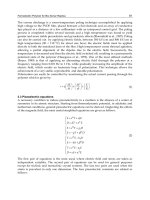
Fig. 1. Diverse applications of flash memory as embedded systems.
Flash Memories
84
The demand for flash memory has reformed its usage to wide areas. For instance, as
illustrated in Figure 1, flash memory is extensively used as embedded systems in several
intelligent and novelty applications such as household appliances, telecommunication
devices, computer applications, automotives and high technology machinery.
2. Flash memory architecture
As shown in Figure 2, flash memory is a block and page based storage device. The page unit
is used to store data where a group of pages is referred to as a block. The page unit is
partitioned into two areas, namely, 1) Data and 2) Spare. The data area is used to store the
actual data while the spare area is used to store the supporting information for the data area
(such as bad block identification, page and block data structures, error correction code
(ECC), etc.). According to present production practices, the page size is fixed from 512 B to 4
KB, while the block size is between 4 KB and 128 KB [18]. Figure 3 shows the attributes of a 4
GB flash memory.
Fig. 2. Block and page layout in flash memory.
There are two different types of flash memory in the current market, namely, 1) NOR-flash,
and 2) NAND-flash [2, 6]. The main distinction between both types is the I/O interface
connection mechanism to the host system. The NOR-flash employs a memory mapped
random access interface with a dedicated address and data lines that are similar to random
access memory (RAM). Besides that, it is a byte-addressable data accessing device that
permits random I/O access with higher performance in reading functionality. On the
contrary, data access in NAND-flash is controlled and managed through two indirect I/O
interface logic methods. They are the emulating block accessing method referred to as the
flash translation layer (FTL) and native file system. The FTL allows physical accessing units
Block Cleaning Process in Flash Memory
85
Fig. 3. Flash memory attributes and specifications.
(block and page) to be addressed as a set of different accessing units (such as 512 B, 2 KB, 4
KB, depending on the manufacturers). In the native file system, the device accessing unit
can directly be accessed without the translation layer. An example of the native file system
employed in NAND-flash is the journaling flash file system (JFFS) [7] and yet another flash
filing system (YAFFS) [23]. For application purposes, the NOR-flash is used for small
amounts of code storage while the NAND-flash is mostly used in data storage applications
since its characteristic are more similar to disk storage.
3. Flash memory characteristics
The characteristics of the flash memory can be summarized as follows [8, 9]:
i. Free accessing time penalties: The flash memory is a semiconductor device which
eliminates the use of mechanical components. This allows the time required to access
data to be uniform, regardless of the data’s location. For instance, let’s say both data a
and data b, which are 4 KB in size each, are randomly located in block i and k (see
Figure 4). The total time required to retrieve data a is 0.088 ms and data b is retrieved
directly after retrieving data a.
Data accessing (retrieving and storing) in flash memory is carried out in three phases, 1)
Setup, 2) Busy, and 3) Data transfer [24]. The accessing command is initialized in the
setup phase. In the busy phase, the required data is temporarily loaded into the flash
memory I/O buffer within a fixed accessing time. Then, the stored data in the I/O
buffer is transferred sequentially to the host system at every fixed serial access time
during the data transfer phase. Similarly, the storing/writing process also requires
constant access time, wherever the location might be.
Flash Memories
86
Fig. 4. Data accessing in flash memory array.
ii. Out-place updating scheme: Data updating in the flash memory is performed via an
out-place scheme rather than an in-place scheme. Due to its EEPROM characteristic, if
the in-place scheme is employed, the block where the updated data is located needs to
be erased first before the data can be restored into the similar location. Furthermore,
block erasure in flash memory is time consuming that can degrade I/O performance.
Thus, the out-place scheme is employed where the updated data is stored into a new
location while its original copy is set as garbage and will not be used any further [10 –
11] (see Figure 5). The main purpose of the out-place scheme is to avoid block erasure
during every update process.
Fig. 5. The out-place updating scheme in the flash memory.
Block Cleaning Process in Flash Memory
87
Due to the out-place scheme, the page in flash memory falls into three states, namely, 1)
Free, 2) Valid, and 3) Invalid. The free state is when a page contains no data and is ready
for storing/writing a new or updated data. The valid state is a page that contains the
current version of the data while the invalid state refers to a page that contains garbage.
In addition, the block status can either be active or inactive [12 – 13] due to the page
states.
iii. Asymmetric accessing time and unit: There are three types of access functions in
flash memory. They are 1) Read, 2) Write/program, and 3) Erase. Each function is
realized in an asymmetric accessing unit and time (see Figure 3). The write function
takes an order of magnitude longer than the read function and both are carried out in
page unit, while the erase function requires the longest access time which is
performed in block unit. The read function fetches a valid data from a valid target
page, while the write function stores data (either new or updated) into a free target
page. On the contrary, the erase function is used to erase an active or an inactive
block with free or invalid pages.
iv. Bulk cleaning with limited block life cycle: The cleaning process is essential in flash
memory due to the employed out-place updating scheme. The cleaning process is
carried out on block unit rather than page unit. The block may contain valid data, thus,
before initiating the process, all valid data residing in the block must be copied out into
available free spaces in other free blocks. However, each block could be tolerant with a
limited number of erasure cycles, for example one million (10
6
) cycles. Exceeding the
erasure cycles will cause the block to become unreliable and spoiled, permanently. For
example, a multi-level cell (MLC) block type typically supports 10,000 erasure cycles. If
the same block is erased and then re-programmed every second, the block would
exceed the 10,000 cycle limit in just three hours. Thus, wear-leveling policy that wears
down all memory blocks as evenly as possible is necessary [14, 15].
4. Cleaning process in flash memory
The cleaning process in flash memory refers to the process of collecting the garbage
scattered throughout the memory array and then reclaiming them back into free space due
to the out-place updating scheme. It is an essential process to guarantee free space
availability on the memory array to ensure new data can be continually stored. However,
the cleaning process is carried out by the erase function and involves bulk size of data rather
than specific locations. The valid data in the block must be copied into the other blocks (free
cells) first, before the cleaning can be initiated. Besides, each flash memory block could
tolerate with an individual erasure lifetime. Frequently erasing blocks causes the blocks to
become unreliable and thus, reduces physical device capacity.
The effectiveness of the cleaning process is heavily dependent on the efficient cleaning
algorithm as well as the data allocation scheme employed by the flash memory system.
Moreover, the cleaning process and the block utilization level are key to the cleaning process
performance and have substantial impact on the access performance, energy consumption
and block endurance [1, 10, 14]. Block utilization is the ratio between valid cells and total
cells and it is represented in percentage. Two categories of cleaning processes in flash
memory are 1) Automatic, and 2) Semi-automatic [16]. Both processes are initiated routinely
by the flash memory controller.
Flash Memories
88
4.1 Automatic cleaning
The automatic cleaning process is automatically commenced when a particular block’s state
in the memory array turns from an active to an inactive (all pages in the block have turned
into invalid state or mixing with several number of free pages). Since there is no valid data
copying process required, the block can be erased in the background during execution of the
current I/O operations (such as read or write) from/into the memory array. Accordingly,
this process requires a constant erase accessing time (E
t
) where the target block ID is given
to the memory controller to erase. Moreover, only a single inactive block (also known as
victim block) can be erased each time the automatic cleaning process is commenced. In
addition, the automatic cleaning process is influence by an efficient data allocation scheme
engaged by the flash memory. There are several data allocation schemes in flash memory
that share identical queuing techniques with a CPU scheduling policy such as first come
first serve (FCFS), first re-arrival first serve (FRFS), online first re-arrival first serve (OFRFS),
and Best Matching (BestM) [12 – 13]. Unlike CPU scheduling policies, the main objective of
the data allocation scheme in the flash memory is to minimize the amount of active blocks
required. The scheme requires the lowest amount of active blocks to minimize the amount
of blocks to be erased when the actual cleaning process is initiated due to the limitation of
the out-place updating scheme.
For example, let’s say file A has been partitioned evenly into five parts (denoted by a, b, c, d,
and e). Assume the accessing pattern of the file is a, b, c, d, a, b, b, a, c, d, a, b, c, d, a, b, d, a, c, c,
d, a, b, c. The snapshot of storing each of the accessed data into the flash memory consisting
of 10 blocks with 4 pages (each, sequentially) is shown in Figure 6. Firstly, the first four
accessed data are stored sequentially in block b
1.
When storing the second accessed data d
(the 10
th
appearance data in the access pattern) into the second free page in block b
3
, block b
1
Fig. 6. Automatic cleaning process in sequential data allocation scheme.