Semiconductor Technologies Part 5 potx
Bạn đang xem bản rút gọn của tài liệu. Xem và tải ngay bản đầy đủ của tài liệu tại đây (4.18 MB, 30 trang )
WetthermaloxidationofGaAsandGaN 113
Pakes et al. (Pakes et al., 2003). They have observed local oxidation and that the oxidation
has occurred at troughs in the faceted GaN layers. Near the peaks in the faceted surface
oxidation was negligible. The localized nature of the oxidation of the GaN is presumed, after
authors, to be related to the strength of the Ga-N bond and non-uniform distributions of
impurity, non-stoichiometry or defects in the substrate (Pakes et al., 2003). The oxide was
non-uniform and textured with pore-like features. The absence of a compact anodic film is
probably due to extensive generation of nitrogen during anodic oxidation which disrupts
development of a uniform anodic film.
Peng et al. (Peng et al., 2001) have patented the method of nitride material oxidation
enhanced by illumination with UV light at room temperature. Authors used 254-nm UV
light to illuminate the GaN crystals to generate electron-hole pairs. The pH value of the
electrolyte was in the range of approximately 3 to 10, preferably about 3.5. The authors
(Peng et al., 2001) claim that: “This invention allows the rapid formation of gallium oxide at room
temperature, and it is possible to monitor the thickness of the oxide in-situ by means of measuring the
loop current.”.
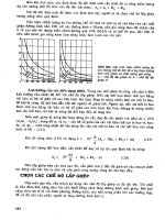
3.3 Plasma oxidation
By plasma oxidation of GaAs gaseous plasma containing oxygen are used. The sources of
oxygen are O
2
, N
2
O or CO
2
, and it is excited by a RF coil (Wilmsen, 1985; Hartnagel &
Riemenschnieder, 1999). A DC bias oxidation takes place in a similar way to the wet
anodization process. In the oxide layers without thermal treatment Ga
2
O
3
and As
2
O
3
almost
in equal proportions were found. Ions which attacked substrate can sputter the surface, and
thus lead to a reduced growth rate and to a modification of surface stoichiometry due to
a preferential sputtering of the arsenic component (Hartnagel & Riemenschnieder, 1999).
The plasma parameters (RF frequency, RF power and gas pressure) may not affect the oxide
growth, but they do affect the degree of GaAs surface degradation during the initial stage of
oxide formation. In contrast, wet anodic oxidations give almost damage-free oxides.
3.4 Dry thermal oxidation
Dry thermal oxidation processes of GaAs and GaN are carried out in ambient of oxygen or
mixture of nitrogen and oxygen. Dry oxidation of GaAs is made rather seldom. Processes
are very complicated because of problems with arsenic and its low thermal stability. Typical
top oxide layers on GaAs surface consist of mixture: Ga
2
O
3
+ GaAsO
4
+ As
2
O
3
and are
rough. Near the interface of oxide-gallium arsenide occur Ga
2
O
3
and elemental As (after:
Wilmsen, 1985). These layers are amorphous. By higher oxidation temperature (above
500 °C) oxides are polycrystalline and also rather rough. They contain mainly Ga
2
O
3
but
GaAsO
4
was also observed. The elemental As, small crystallites of As
2
O
5
and As
2
O
3
appeared in layers as well (after: Pessegi et al., 1998). Arsenic oxides have low thermal
stability and during annealing processes oxides undergo decomposition releasing arsenic
which escapes from the samples.
Thermal oxidation of GaAs technique has more than thirty years. Thermal oxidation of GaN
epilayers is a considerably younger – it is a matter of last ten years.
Gallium nitride needs higher temperature as GaAs or AlAs: typical range of dry oxidation is
between 800 and 1100 °C (Chen et al., 2000). Processes are carried out usually in atmosphere
of oxygen (Chen et al., 2000; Lin et al., 2006). Chen at al. (Chen et al., 2000) described several
experiments with GaN layers on sapphire substrates. Authors made oxidation of GaN
samples in dry oxygen. Time of oxidation was changed from 20 min to 8 h by the flow of O
2
of about 1 slm. Temperature was changed from 800 to 1100 °C. They have observed two
different courses for temperatures of over 1000 °C: very rapid oxidation process in the initial
stage of oxidation and then, after about 1 h, followed by a relatively slow process. Authors
have deliberated after Wolter et al. (Wolter et al., 1998) the reaction rate constant and have
concluded that in the first step of oxidation (rapid process) the oxide creation reaction is
limited by the rate of reaction on GaN-oxide interface. In second step (slow process by
thicker oxide layers) the oxide creation reaction is determined by the diffusion-controlled
mechanism (transition from reaction-controlled mechanism to the diffusion-controlled
mechanism). They have supposed GaN decomposition at high temperature (over 1000 °C)
which can speed up the gallium oxidation (Chen et al., 2000). The authors also have
observed volume increase of about 40% after oxidation.
Similar experiments were made by Zhou et al. (Zhou et al., 2008) by oxidation of GaN
powder and GaN free-standing substrates with Ga-terminated surface (front side) from
HVPE epitaxial processes. They have used dry oxygen as a reactor chamber atmosphere
only and have changed time (from 4 to 12 hours) and temperature (850, 900, 950 and 950 °C)
of oxidation. According to authors, oxidation rate in temperature below 750 °C is negligible.
They have made similar analysis as Chen et al. (Chen et al., 2000) after Wolter et al. (Wolter
et al., 1998) and observed similar dependence of the oxide thickness versus time process. In
GaN dry oxidation processes one could observe two zones: interfacial reaction-controlled
and diffusion-controlled mechanism for low and high temperature, respectively (Zhou et al.,
2008). Authors of this paper have wrote about “thermally grown gallium oxide on ( ) GaN
substrate”. It is typical for many authors although all of them described oxidation process.
3.5 Wet thermal oxidation
Problems in wet thermal oxidation of GaAs processes are very similar to those which occur
during dry oxidation. Arsenic in GaAs has low thermal stability in high temperature and it
is rather difficult to carry out oxidation process at the temperature higher than 600 °C. The
applied temperatures from the range below 600 °C gave not rewarding results. The obtained
by Korbutowicz et al. (Korbutowicz et al., 2008) gallium oxide layers have been very thin
and had have weak adhesion.
Processes of wet thermal GaN oxidation are carried out more often. Gallium nitride has
better thermal stability than gallium arsenide and one can apply higher temperature to
obtained Ga
2
O
3
is thicker and has better parameters.
Typical apparatus for wet thermal oxidation of GaAs or GaN is very similar to that which is
applied to wet thermal oxidation of AlAs or Al
x
Ga
1-x
As. It can be: Closed Chamber System
CCS (a) or Open Chamber System OCS (b). The open systems are more often used as the
systems with closed tube one.
3.5.1 Close chamber systems
Choe et al. have described in their paper (Choe et al., 2000) CCS equipment for AlAs
oxidation which was schematically depicted in Figure 5 a. It also can be applied to GaAs
oxidation. The quartz reaction (oxidation) chamber had two temperature zones – the upper
and lower zone, one for the sample and second for the water source. It was small chamber –
SemiconductorTechnologies114
3 cm in diameter by 30 cm in length. Typical amount of water was about 2 cm
3
. Chamber
with sample and water was closed and the air was evacuated using a pump. After this
hermetically closed chamber was inserted into a furnace. During the heating, water was
expanded as a vapour and filled whole volume of the quartz ampoule. Typical temperature
in the upper zone was 410 °C and in the lower zone was varied from 80 °C to 220 °C. In this
apparatus the oxidation process is controlled by two parameters: temperature of oxidation
and temperature of water source.
These systems have some advantages: reaction kinetics in controlled by two temperatures:
oxidation and water vapour creation, there is a small demand of oxidizing agent – water and
no carrier gas. A considerable inconvenience is the necessity of vacuum pumps application.
3.5.2 Open chamber systems
Open chamber system for GaAs and GaN oxidation looks like silicon oxidation system. It
consists of horizontal (very often) quartz tube, water bubbler and source of the gases: carrier
– nitrogen N
2
or argon Ar and (sometimes) oxygen O
2
(Choquette et al., 1997; Readinger et
al., 1999; Pucicki et al., 2004; Geib et al., 2007; Korbutowicz et al., 2008). The three-zone
resistant furnace works as a system heating (Fig. 5 b). Korbutowicz et al. (Korbutowicz et al.,
2008) have used the bubbler (in the heating jacket with a temperature control) with
deionized water H
2
O as a source of oxidizing agent and nitrogen N
2
as a main gas and the
initial water level was the same in all experiments to keep the same conditions of the carrier
gas saturation.
(a)
(b)
N
2
3-zone furnace
heater with temperature control
bubbler with DI water
thermocouple
rotameters
reactor chamber
Fig. 5. (a) A schematic diagram of the CCS for wet thermal oxidation (Choe et al., 2000); (b)
typical apparatus for GaAs and GaN wet thermal oxidation
The open systems are cheaper as the closed ones. The work with the OCS’s are more
complicated – one need to take into consideration numerous parameters: source water
temperature, reaction temperature, main gas flow and flow of the carrier gas through the
bubbler, kind of gases and using or not of oxygen. The significant water consumption
during oxidation and the requirement of the water source temperature stabilization also
constitute problems. But the valuable advantage of open systems is their simple
construction.
Thermal wet oxidation method as a more frequently applied way to get gallium oxide layers
will be wider described now.
Reaction kinetics of thermal wet oxidation and reaction results depend on several
parameters: a zone reaction temperature (a), a water source temperature (water bubbler) (b),
a flow of a main currier gas (c), a flow of a carrier gas through the water bubbler (d), time of
the reaction (e) and type of currier gas (f).
Korbutowicz et al. (Korbutowicz et al., 2008) have described processes of the GaAs and GaN
thermal wet oxidation – GaAs wafers and GaN layers manufactured by MOVPE and HVPE
(Hydride Vapor Phase Epitaxy) on sapphire substrates were used in these studies. GaAs in
form of bare wafers (one side polished, Te doped) or wafers with epilayers (Si doped) were
employed in investigations. A range of oxidation temperature was between 483 and 526 °C.
Time was varied from 60 to 300 minutes. Typical main flow of nitrogen was 2 800 sccm/min
and typical flows through the water bubbler were 260 and 370 sccm/min.
Thicknesses of the gallium oxides layers grown on gallium arsenide substrates surface were
uneven – it was visible to the naked eye: one can observed variable colors on the surface (see
Fig. 6 (a)). Defects are preferable points to create oxide – from these spots started the
oxidation process (Fig. 6 (b)). Authors were able to obtain thin layers only, since by longer
process duration oxide layers were cracked and exfoliated. In Fig. 6 (c) one can see that
oxide layers were thin and transparent. Occurring cracks show that in interface region of
GaAs-oxide exists a considerable strain.
(a)
(b)
(c)
Fig. 6. Views of oxide surface’s layers from optical microscope: variable colors of gallium
oxide (a); substrate’s defect and oxide (b); cracked and exfoliated oxide layer (c)
Two kinds of GaN samples have been used – GaN epilayers deposited on sapphire
substrates – thin layers from MOVPE and thick layers from HVPE with surface as grown.
Temperature of oxidation was higher as for GaAs samples and was as follows: 755, 795 and
827 °C. Typical water temperature was 95 or 96 °C. The main flows of nitrogen were varied
from 1 450 to 2 800 sccm/min and the flows through the water bubbler were altered from
260 to 430 sccm/min. The total gas flow in the reactor chamber was about 3 000 sccm/min.
In order to determine suitable parameters, temperature of water source and temperature of
reaction (oxidation) zone were changed. Gas flows and time of the process were varied also.
The obtained thicknesses of gallium oxide were from several nanometers up to hundreds of
nanometers. The MOVPE GaN layers has much more smoother surface as from HVPE ones.
The influence of this difference one can remark after oxidation.
Optical observations by using naked eyes and optical microscope gave a lot of information
about morphology of surface with oxide. One can observe (Fig. 7.) e.g. smoothing of GaN
hexagonal islands. Wet oxidation of gallium arsenide appeared to be more difficult than that
of GaN. The Ga
2
O
3
layers which were obtained by Korbutowicz et al. were heterogeneous
(see below results from X-ray diffraction – Fig. 8).
WetthermaloxidationofGaAsandGaN 115
3 cm in diameter by 30 cm in length. Typical amount of water was about 2 cm
3
. Chamber
with sample and water was closed and the air was evacuated using a pump. After this
hermetically closed chamber was inserted into a furnace. During the heating, water was
expanded as a vapour and filled whole volume of the quartz ampoule. Typical temperature
in the upper zone was 410 °C and in the lower zone was varied from 80 °C to 220 °C. In this
apparatus the oxidation process is controlled by two parameters: temperature of oxidation
and temperature of water source.
These systems have some advantages: reaction kinetics in controlled by two temperatures:
oxidation and water vapour creation, there is a small demand of oxidizing agent – water and
no carrier gas. A considerable inconvenience is the necessity of vacuum pumps application.
3.5.2 Open chamber systems
Open chamber system for GaAs and GaN oxidation looks like silicon oxidation system. It
consists of horizontal (very often) quartz tube, water bubbler and source of the gases: carrier
– nitrogen N
2
or argon Ar and (sometimes) oxygen O
2
(Choquette et al., 1997; Readinger et
al., 1999; Pucicki et al., 2004; Geib et al., 2007; Korbutowicz et al., 2008). The three-zone
resistant furnace works as a system heating (Fig. 5 b). Korbutowicz et al. (Korbutowicz et al.,
2008) have used the bubbler (in the heating jacket with a temperature control) with
deionized water H
2
O as a source of oxidizing agent and nitrogen N
2
as a main gas and the
initial water level was the same in all experiments to keep the same conditions of the carrier
gas saturation.
(a)
(b)
N
2
3-zone furnace
heater with temperature control
bubbler with DI water
thermocouple
rotameters
reactor chamber
Fig. 5. (a) A schematic diagram of the CCS for wet thermal oxidation (Choe et al., 2000); (b)
typical apparatus for GaAs and GaN wet thermal oxidation
The open systems are cheaper as the closed ones. The work with the OCS’s are more
complicated – one need to take into consideration numerous parameters: source water
temperature, reaction temperature, main gas flow and flow of the carrier gas through the
bubbler, kind of gases and using or not of oxygen. The significant water consumption
during oxidation and the requirement of the water source temperature stabilization also
constitute problems. But the valuable advantage of open systems is their simple
construction.
Thermal wet oxidation method as a more frequently applied way to get gallium oxide layers
will be wider described now.
Reaction kinetics of thermal wet oxidation and reaction results depend on several
parameters: a zone reaction temperature (a), a water source temperature (water bubbler) (b),
a flow of a main currier gas (c), a flow of a carrier gas through the water bubbler (d), time of
the reaction (e) and type of currier gas (f).
Korbutowicz et al. (Korbutowicz et al., 2008) have described processes of the GaAs and GaN
thermal wet oxidation – GaAs wafers and GaN layers manufactured by MOVPE and HVPE
(Hydride Vapor Phase Epitaxy) on sapphire substrates were used in these studies. GaAs in
form of bare wafers (one side polished, Te doped) or wafers with epilayers (Si doped) were
employed in investigations. A range of oxidation temperature was between 483 and 526 °C.
Time was varied from 60 to 300 minutes. Typical main flow of nitrogen was 2 800 sccm/min
and typical flows through the water bubbler were 260 and 370 sccm/min.
Thicknesses of the gallium oxides layers grown on gallium arsenide substrates surface were
uneven – it was visible to the naked eye: one can observed variable colors on the surface (see
Fig. 6 (a)). Defects are preferable points to create oxide – from these spots started the
oxidation process (Fig. 6 (b)). Authors were able to obtain thin layers only, since by longer
process duration oxide layers were cracked and exfoliated. In Fig. 6 (c) one can see that
oxide layers were thin and transparent. Occurring cracks show that in interface region of
GaAs-oxide exists a considerable strain.
(a)
(b)
(c)
Fig. 6. Views of oxide surface’s layers from optical microscope: variable colors of gallium
oxide (a); substrate’s defect and oxide (b); cracked and exfoliated oxide layer (c)
Two kinds of GaN samples have been used – GaN epilayers deposited on sapphire
substrates – thin layers from MOVPE and thick layers from HVPE with surface as grown.
Temperature of oxidation was higher as for GaAs samples and was as follows: 755, 795 and
827 °C. Typical water temperature was 95 or 96 °C. The main flows of nitrogen were varied
from 1 450 to 2 800 sccm/min and the flows through the water bubbler were altered from
260 to 430 sccm/min. The total gas flow in the reactor chamber was about 3 000 sccm/min.
In order to determine suitable parameters, temperature of water source and temperature of
reaction (oxidation) zone were changed. Gas flows and time of the process were varied also.
The obtained thicknesses of gallium oxide were from several nanometers up to hundreds of
nanometers. The MOVPE GaN layers has much more smoother surface as from HVPE ones.
The influence of this difference one can remark after oxidation.
Optical observations by using naked eyes and optical microscope gave a lot of information
about morphology of surface with oxide. One can observe (Fig. 7.) e.g. smoothing of GaN
hexagonal islands. Wet oxidation of gallium arsenide appeared to be more difficult than that
of GaN. The Ga
2
O
3
layers which were obtained by Korbutowicz et al. were heterogeneous
(see below results from X-ray diffraction – Fig. 8).
SemiconductorTechnologies116
Fig. 7. HVPE GaN layer surface after wet thermal oxidation
Figure 8. shows x-ray spectrum of gallium compounds on sapphire substrate (G32 sample).
One can remark that oxidized surface layer contained GaN, Ga
2
O
3
and Ga
x
NO
y
.
Fig. 8. X-ray diffraction spectrum of oxidized GaN on sapphire from HVPE; G32_SMT2 –
spectrum from thick GaN layer
The MOVPE GaN crystals had smoother surface as HVPE crystals and were more resistant
for oxidation. In Figure 9 results of AFM (Atomic Force Microscope) observations of the
surface and profile of MOVPE sample, thickness of 880 (nm) (a) and HVPE sample,
thickness of 12 (µm) (b) are shown. Both samples were oxidized in the same conditions:
reaction temperature of 827 °C, water source temperature of 95 °C, process time of 120 min
and the same water vapour concentration. The initial surface of MOVPE sample was
smooth, while the surface of HVPE thick layers was rather rough. The oxidation process was
faster by HVPE crystals because at these crystals surfaces was more developed. The surface
of oxidized GaN from MOVPE remained smooth, whereas on the surface of the sample from
HVPE one could observe typical little bumps.
(a)
(b)
Fig. 9. AFM images of the surface of GaN
(MOVPE)
sample (a) and GaN
(HVPE)
sample (b)
Readinger et al. (Readinger et al., 1999) have carried out processes applying GaN powder
and GaN thick layers on sapphire from vertical HVPE. Atomic percentage of water vapor in
carrier gas (O
2
, N
2
, and Ar) was maintained on the same level (77%8%) for all furnace
temperatures (700, 750, 800, 850 and 900 °C) and carrier gas combinations. For comparison
purposes authors have prepared a dry oxidation processes (in dry oxygen) for the same
samples. Sample’s surfaces after wet oxidation were much smoother as from dry process.
The authors have observed that below 700 °C in which GaN has a good stability in oxidizing
environments. They also have found that in ambient of oxygen (dry or wet) the oxidation
had faster rate as in wet nitrogen or argon atmosphere. Thicknesses of gallium oxide layers
in wet O
2
process revealed linear dependence on duration of oxidation. Wet oxidation have
given even poorer electrical results than dry oxidation. The authors have judged that
electrical parameters deterioration aroused from very irregular morphology at the wet
oxide/GaN interface.
3.6 Other oxidation methods
These above mentioned oxidation methods are not the only ways to get gallium oxide.
There are several others ones:
ion-beam induced oxidation (after: Hartnagel & Riemenschnieder, 1999),
laser assisted oxidation (Bermudez, 1983),
low-temperature oxidation (after: Hartnagel & Riemenschnieder, 1999),
photowash oxidation (Offsay et al., 1986),
oxidation by an atomic oxygen beam (after: Hartnagel & Riemenschnieder, 1999),
UV/ozone oxidation (after: Hartnagel & Riemenschnieder, 1999),
vacuum ultraviolet photochemical oxidation (Yu et al., 1988).
3.7 Summary
Apart from above mentioned methods are several other ways to obtain or manufacture
gallium oxide layers. One can deposited by Chemical Vapour Deposition CVD, Physical
Vapour Deposition PVD or Physical Vapour Transport PVT methods. One can use Local
Anodic Oxidation LAO by applying AFM equipment (Matsuzaki et al., 2000; Lazzarino et
al., 2005; Lazzarino et al., 2006) to GaAs or GaN surface oxidizing and creating small regions
WetthermaloxidationofGaAsandGaN 117
Fig. 7. HVPE GaN layer surface after wet thermal oxidation
Figure 8. shows x-ray spectrum of gallium compounds on sapphire substrate (G32 sample).
One can remark that oxidized surface layer contained GaN, Ga
2
O
3
and Ga
x
NO
y
.
Fig. 8. X-ray diffraction spectrum of oxidized GaN on sapphire from HVPE; G32_SMT2 –
spectrum from thick GaN layer
The MOVPE GaN crystals had smoother surface as HVPE crystals and were more resistant
for oxidation. In Figure 9 results of AFM (Atomic Force Microscope) observations of the
surface and profile of MOVPE sample, thickness of 880 (nm) (a) and HVPE sample,
thickness of 12 (µm) (b) are shown. Both samples were oxidized in the same conditions:
reaction temperature of 827 °C, water source temperature of 95 °C, process time of 120 min
and the same water vapour concentration. The initial surface of MOVPE sample was
smooth, while the surface of HVPE thick layers was rather rough. The oxidation process was
faster by HVPE crystals because at these crystals surfaces was more developed. The surface
of oxidized GaN from MOVPE remained smooth, whereas on the surface of the sample from
HVPE one could observe typical little bumps.
(a)
(b)
Fig. 9. AFM images of the surface of GaN
(MOVPE)
sample (a) and GaN
(HVPE)
sample (b)
Readinger et al. (Readinger et al., 1999) have carried out processes applying GaN powder
and GaN thick layers on sapphire from vertical HVPE. Atomic percentage of water vapor in
carrier gas (O
2
, N
2
, and Ar) was maintained on the same level (77%8%) for all furnace
temperatures (700, 750, 800, 850 and 900 °C) and carrier gas combinations. For comparison
purposes authors have prepared a dry oxidation processes (in dry oxygen) for the same
samples. Sample’s surfaces after wet oxidation were much smoother as from dry process.
The authors have observed that below 700 °C in which GaN has a good stability in oxidizing
environments. They also have found that in ambient of oxygen (dry or wet) the oxidation
had faster rate as in wet nitrogen or argon atmosphere. Thicknesses of gallium oxide layers
in wet O
2
process revealed linear dependence on duration of oxidation. Wet oxidation have
given even poorer electrical results than dry oxidation. The authors have judged that
electrical parameters deterioration aroused from very irregular morphology at the wet
oxide/GaN interface.
3.6 Other oxidation methods
These above mentioned oxidation methods are not the only ways to get gallium oxide.
There are several others ones:
ion-beam induced oxidation (after: Hartnagel & Riemenschnieder, 1999),
laser assisted oxidation (Bermudez, 1983),
low-temperature oxidation (after: Hartnagel & Riemenschnieder, 1999),
photowash oxidation (Offsay et al., 1986),
oxidation by an atomic oxygen beam (after: Hartnagel & Riemenschnieder, 1999),
UV/ozone oxidation (after: Hartnagel & Riemenschnieder, 1999),
vacuum ultraviolet photochemical oxidation (Yu et al., 1988).
3.7 Summary
Apart from above mentioned methods are several other ways to obtain or manufacture
gallium oxide layers. One can deposited by Chemical Vapour Deposition CVD, Physical
Vapour Deposition PVD or Physical Vapour Transport PVT methods. One can use Local
Anodic Oxidation LAO by applying AFM equipment (Matsuzaki et al., 2000; Lazzarino et
al., 2005; Lazzarino et al., 2006) to GaAs or GaN surface oxidizing and creating small regions
SemiconductorTechnologies118
covered by gallium oxide. As was told earlier in chapter 2, the best parameters for
semiconductor devices has monoclinic -Ga
2
O
3
. This type of oxide is easy to obtain by
thermal oxidation: dry or wet. These methods also give possibility to selective oxidation
using dielectric mask (e.g. SiO
2
). Despite the difficulties and problems on account of
numerous process parameters which ought to be taken into consideration, wet thermal
oxidation of GaAs and GaN processes seem to be the best way for making oxide layers for
devices applications.
4. Applications of gallium oxide structures in electronics
Due to existent of native silicon oxide domination of silicon in electronics lasts many years.
Semiconductor compounds as AIIIBV or AIIIN have very good parameters which just
predestine to work in a region of high frequencies and a high temperature with a high
power: insulating substrates, high carrier mobility and wide bandgap. These all give a big
advantage over Si and their alloys. But silicon still dominates. Why?
SiO
2
is an amorphous material which does not bring strain in underlying silicon. Gallium
arsenide GaAs applied in semiconductor devices technology has cubic crystal structure (as
other AIIIBV compounds) and typical surface orientation (100). Gallium oxide with
monoclinic structure, which is the only variety of Ga
2
O
3
stable in high temperature that
stays stable after cooling, is strongly mismatched to GaAs. It causes bad relationships
between GaAs epitaxial layers and oxide. In addition, gallium oxide growth on a surface of
gallium arsenide is in a reality a mixture of Ga
2
O
3
, As
2
O
3
, As
2
O
5
and elemental As, as was
mentioned above. This mixture is unstable at elevated temperature and has poor dielectric
parameters. In order to avoid problems with the growth of Ga
2
O
3
on GaAs surface some of
researches have applied thin dielectric layer of Al
2
O
3
in GaAs MOSFET structure (e.g. Jun,
2000) but it is not a matter of our consideration.
By GaN oxidation is other situation than by GaAs treatment. Gallium nitride applied in
electronics has hexagonal structure and is better matched. GaN, in comparison to GaAs, is
more chemical, thermal and environmental resistant. Therefore nitrides are more often used
to construction of numerous devices with a oxide-semiconductor structure: MOS diodes and
transistors, gas and chemical sensors.
Silicon electronics supremacy was a result of, among others, applying of silicon oxide SiO
2
possibility. Properties of interface silicon oxide and silicon are just excellent. This fact allows
manufacturing of very-large scale integration circuits with Complementary Metal Oxide
Semiconductor (CMOS) transistors (Hong, 2008). But silicon devices encounter difficulties
going to nanoscale – very thin dielectric gate layers is too thin and there is no effect: charge
carriers can flow through the gate dielectric by the quantum mechanical tunnelling
mechanism. Leakage current is too high – Si devices need dielectrics with higher electrical
permittivity k. Also power devices made from silicon and their alloys operate in smaller
range of power and frequency. One can draw a conclusion: MOS devices need high k gate
dielectric and carriers with higher mobility in channels of transistors as in silicon’s ones.
Whole microelectronics requires something else, for example indium phosphide, diamond,
silicon carbide, gallium arsenide or gallium nitride and their alloys (see Fig. 10 (Kasu, 2004)).
Fig. 10. Demand for high-frequency high-power semiconductors to support the rise in
communication capacity (Kasu, 2004)
Despite very good properties, AIIIBV and AIIIN have problems to become commonly used,
especially in power applications. A big obstacle is a lack of high quality stable gate
dielectrics with high value of dielectric constant. In opinion Ye (Ye, 2008): “The physics and
chemistry of III–V compound semiconductor surfaces or interfaces are problems so complex that our
understanding is still limited even after enormous research efforts.” and that can be the purpose
although first GaAs MOSFETs was reported by Becke and White in 1965 (after: Ye, 2008) still
there are problems with wide scale production.
One can deposit silicon dioxide, silicon nitride and similar dielectrics but these materials
have relatively small dielectric constant. SiO
2
has dielectric constant equal to 3.9, Si
3
N
4
has
constant = 7.5, but silicon nitride is not easy in a treatment. Typical value of dielectric
constant given in literature for Ga
2
O
3
is in a range from 9.9 to 14.2 (Passlack et al., 1995;
Pearton et al., 1999).
4.1 Metal Oxide Semiconductor devices
The first thermal-oxide gate GaAs MOSFET was reported in the work of Takagi et al. in 1978
(Takagi et al., 1978). The gate oxide, which has been grown by the new GaAs oxidation
technique in the As
2
O
3
vapor, was chemically stable. Oxidation process was carried out in
a closed quartz ampoule. Temperature of liquid arsenic trioxide was equal to 470 °C and
temperature of GaAs (gallium oxide growth) was 500 °C. Authors supposed that this
method can be used in large scale as a fabrication process. But up to now it is not the typical
manufacture technique.
Typical GaAs MOSFET has the gate dielectric in the form of oxides mixture: Ga
2
O
3
(Gd
2
O
3
).
This mixture comes not from oxidation but from UHV deposition (e.g. Passlack, et al. 1997;
Hong et al., 2007; Passlack et al., 2007). Practically almost all papers of Passlack’s team from
the last twenty years have described oxide structures this type: Ga
2
O
3
(Gd
2
O
3
) which were
made in UHV apparatus.
Difficulties with obtaining good Ga
2
O
3
layers on GaAs from thermal oxidation inclined
researches to make GaAs MOS structures with oxidized thin layer of AlGaAs or InAlP but
then aluminium is oxidized, not gallium (e.g. Jing et al., 2008).
Matter of the GaN MOS structures looks similar and different too. In many cases gate
dielectric is Gadolinium Gallium Garnet (GGG) Gd
3
Ga
5
O
12
called also Gadolinium Gallium
WetthermaloxidationofGaAsandGaN 119
covered by gallium oxide. As was told earlier in chapter 2, the best parameters for
semiconductor devices has monoclinic -Ga
2
O
3
. This type of oxide is easy to obtain by
thermal oxidation: dry or wet. These methods also give possibility to selective oxidation
using dielectric mask (e.g. SiO
2
). Despite the difficulties and problems on account of
numerous process parameters which ought to be taken into consideration, wet thermal
oxidation of GaAs and GaN processes seem to be the best way for making oxide layers for
devices applications.
4. Applications of gallium oxide structures in electronics
Due to existent of native silicon oxide domination of silicon in electronics lasts many years.
Semiconductor compounds as AIIIBV or AIIIN have very good parameters which just
predestine to work in a region of high frequencies and a high temperature with a high
power: insulating substrates, high carrier mobility and wide bandgap. These all give a big
advantage over Si and their alloys. But silicon still dominates. Why?
SiO
2
is an amorphous material which does not bring strain in underlying silicon. Gallium
arsenide GaAs applied in semiconductor devices technology has cubic crystal structure (as
other AIIIBV compounds) and typical surface orientation (100). Gallium oxide with
monoclinic structure, which is the only variety of Ga
2
O
3
stable in high temperature that
stays stable after cooling, is strongly mismatched to GaAs. It causes bad relationships
between GaAs epitaxial layers and oxide. In addition, gallium oxide growth on a surface of
gallium arsenide is in a reality a mixture of Ga
2
O
3
, As
2
O
3
, As
2
O
5
and elemental As, as was
mentioned above. This mixture is unstable at elevated temperature and has poor dielectric
parameters. In order to avoid problems with the growth of Ga
2
O
3
on GaAs surface some of
researches have applied thin dielectric layer of Al
2
O
3
in GaAs MOSFET structure (e.g. Jun,
2000) but it is not a matter of our consideration.
By GaN oxidation is other situation than by GaAs treatment. Gallium nitride applied in
electronics has hexagonal structure and is better matched. GaN, in comparison to GaAs, is
more chemical, thermal and environmental resistant. Therefore nitrides are more often used
to construction of numerous devices with a oxide-semiconductor structure: MOS diodes and
transistors, gas and chemical sensors.
Silicon electronics supremacy was a result of, among others, applying of silicon oxide SiO
2
possibility. Properties of interface silicon oxide and silicon are just excellent. This fact allows
manufacturing of very-large scale integration circuits with Complementary Metal Oxide
Semiconductor (CMOS) transistors (Hong, 2008). But silicon devices encounter difficulties
going to nanoscale – very thin dielectric gate layers is too thin and there is no effect: charge
carriers can flow through the gate dielectric by the quantum mechanical tunnelling
mechanism. Leakage current is too high – Si devices need dielectrics with higher electrical
permittivity k. Also power devices made from silicon and their alloys operate in smaller
range of power and frequency. One can draw a conclusion: MOS devices need high k gate
dielectric and carriers with higher mobility in channels of transistors as in silicon’s ones.
Whole microelectronics requires something else, for example indium phosphide, diamond,
silicon carbide, gallium arsenide or gallium nitride and their alloys (see Fig. 10 (Kasu, 2004)).
Fig. 10. Demand for high-frequency high-power semiconductors to support the rise in
communication capacity (Kasu, 2004)
Despite very good properties, AIIIBV and AIIIN have problems to become commonly used,
especially in power applications. A big obstacle is a lack of high quality stable gate
dielectrics with high value of dielectric constant. In opinion Ye (Ye, 2008): “The physics and
chemistry of III–V compound semiconductor surfaces or interfaces are problems so complex that our
understanding is still limited even after enormous research efforts.” and that can be the purpose
although first GaAs MOSFETs was reported by Becke and White in 1965 (after: Ye, 2008) still
there are problems with wide scale production.
One can deposit silicon dioxide, silicon nitride and similar dielectrics but these materials
have relatively small dielectric constant. SiO
2
has dielectric constant equal to 3.9, Si
3
N
4
has
constant = 7.5, but silicon nitride is not easy in a treatment. Typical value of dielectric
constant given in literature for Ga
2
O
3
is in a range from 9.9 to 14.2 (Passlack et al., 1995;
Pearton et al., 1999).
4.1 Metal Oxide Semiconductor devices
The first thermal-oxide gate GaAs MOSFET was reported in the work of Takagi et al. in 1978
(Takagi et al., 1978). The gate oxide, which has been grown by the new GaAs oxidation
technique in the As
2
O
3
vapor, was chemically stable. Oxidation process was carried out in
a closed quartz ampoule. Temperature of liquid arsenic trioxide was equal to 470 °C and
temperature of GaAs (gallium oxide growth) was 500 °C. Authors supposed that this
method can be used in large scale as a fabrication process. But up to now it is not the typical
manufacture technique.
Typical GaAs MOSFET has the gate dielectric in the form of oxides mixture: Ga
2
O
3
(Gd
2
O
3
).
This mixture comes not from oxidation but from UHV deposition (e.g. Passlack, et al. 1997;
Hong et al., 2007; Passlack et al., 2007). Practically almost all papers of Passlack’s team from
the last twenty years have described oxide structures this type: Ga
2
O
3
(Gd
2
O
3
) which were
made in UHV apparatus.
Difficulties with obtaining good Ga
2
O
3
layers on GaAs from thermal oxidation inclined
researches to make GaAs MOS structures with oxidized thin layer of AlGaAs or InAlP but
then aluminium is oxidized, not gallium (e.g. Jing et al., 2008).
Matter of the GaN MOS structures looks similar and different too. In many cases gate
dielectric is Gadolinium Gallium Garnet (GGG) Gd
3
Ga
5
O
12
called also Gadolinium Gallium
SemiconductorTechnologies120
Oxide (GGO), a synthetic crystalline material of the garnet group or Ga
2
O
3
(Gd
2
O
3
) (e.g. Gila
et al., 2000) as by GaAs MOSFETs. Some researches tried to make Ga
2
O
3
layer on GaN as
dielectric film for MOS applications: MOS capacitors (Kim et al., 2001; Nakano & Jimbo,
2003) or MOS diodes (Nakano a et al., 2003).
Kim et al. (Kim et al., 2001) were studied dry thermal oxidation of GaN in ambient of
oxygen. It was a furnace oxidation at 850 °C for 12 h which resulted in the formation of
monoclinic -Ga
2
O
3
layer, 88 nm in thickness. Authors have analyzed the structural
properties of the oxidized sample by SEM (scanning electron microscopy), XRD and AES
(Auger Electron Spectroscopy) measurements. In order to develop the electrical
characteristics of the thermally oxidized GaN film, a MOS capacitor was fabricated. Based
on observations and measurements, authors have found that: (i) the formation of monoclinic
-Ga
2
O
3
occurred, (ii) the breakdown field strength of the thermal oxide was 3.85 MVcm
-1
and, (iii) the C–V curves showed a low oxide charge density (N
f
) of 6.7710
11
cm
-2
. After Kim
et al. it suggests that the thermally grown Ga
2
O
3
is promising for GaN-based power
MOSFET applications (Kim et al.; 2001).
Nakano & Jimbo (Nakano & Jimbo, 2003) have described their study on the interface
properties of thermally oxidized n type GaN metal–oxide–semiconductor capacitors
fabricated on sapphire substrates. A 100 nm thick -Ga
2
O
3
was grown by dry oxidation at
880 °C for 5 h. After epitaxial growth, authors have made typical lateral dot-and-ring -
Ga
2
O
3
/GaN MOS capacitors by a thermal oxidation method. In order to reach this aim a 500
nm thick Si layer was deposited on the top surface of the GaN sample as a mask material for
thermal oxidation. Formation of monoclinic -Ga
2
O
3
was confirmed by XRD. They have also
observed from SIMS (secondary ion mass spectrometry) measurements, an intermediate Ga
oxynitride layer with graded compositions at the -Ga
2
O
3
/GaN interface (see Fig. 11). The
presence of GaNO was remarked by Korbutowicz et al. (Korbutowicz et al., 2008) in samples
from the wet thermal oxidation after XRD measurements as well. Nakano & Jimbo (Nakano
& Jimbo, 2003) have not observed in the C– t and DLTS (Deep Level Transient Spectroscopy)
measurements discrete interface traps. They have judged that it is in reasonable agreement
with the deep depletion feature and low interface state density of 5.5310
10
eV
-1
cm
-2
revealed by the C–V measurements. They have supposed that the surface Fermi level can
probably be unpinned at the -Ga
2
O
3
/GaN MOS structures fabricated by a thermal
oxidation technique. The authors have compared as well the sputtered SiO
2
/GaN MOS and
-Ga
2
O
3
/GaN MOS samples in DLTS measurements. In Fig. 12 results of this study were
shown. In contrast to the -Ga
2
O
3
/GaN MOS structure, SiO
2
/GaN MOS sample has a large
number of interface traps may induce the surface Fermi-level pinning at the MOS interface,
resulting in the capacitance saturation observed in the deep depletion region of the C–V
curve (Nakano & Jimbo, 2003).
In slightly later publication of Nakano et. al. (Nakano a et al., 2003) have described electrical
properties of thermally oxidized p-GaN MOS diodes with n
+
source regions fabricated on
Al
2
O
3
substrates. Oxide was grown in the same way as in paper (Nakano & Jimbo, 2003).
Results obtained by authors in this study have suggested that the thermally grown -
Ga
2
O
3
/p-GaN MOS structure is a promising candidate for inversion-mode MOSFET.
Fig. 11. SIMS profiles of Ga, N, and O atoms in the thermally oxidized -Ga
2
O
3
/GaN MOS
structure (Nakano & Jimbo, 2003).
Fig. 12. Typical DLTS spectra at a rate window t
1
/t
2
of 10 ms/20 ms for the thermally
oxidized -Ga
2
O
3
/GaN MOS and sputtered SiO
2
/n-GaN MOS structures after applying the
bias voltage of 225 V (Nakano & Jimbo, 2003).
Lin et al. (Lin et al., 2006) have studied the influence of oxidation and annealing temperature
on quality of Ga
2
O
3
grown on GaN. GaN wafers were oxidized at 750 °C, 800 °C and 850 °C.
Authors have measured the electrical characteristics and interface quality of the resulting
MOS capacitors have compared. The process steps for making GaN MOS capacitor is shown
in Fig. 13. The 300-nm SiO
2
layer was deposited on the GaN surface by radio-frequency
sputtering to play as a mask for oxidation.
(1) (2) (3) (4) (5) (6)
Fig. 13. Process flow for GaN MOS capacitor (Lin et al., 2006)
Oxidation was carried out in dry oxygen ambient and followed by a 0.5 h annealing in
argon at the same temperature as oxidation. GaN oxidized at a higher temperature of 850 °C
WetthermaloxidationofGaAsandGaN 121
Oxide (GGO), a synthetic crystalline material of the garnet group or Ga
2
O
3
(Gd
2
O
3
) (e.g. Gila
et al., 2000) as by GaAs MOSFETs. Some researches tried to make Ga
2
O
3
layer on GaN as
dielectric film for MOS applications: MOS capacitors (Kim et al., 2001; Nakano & Jimbo,
2003) or MOS diodes (Nakano a et al., 2003).
Kim et al. (Kim et al., 2001) were studied dry thermal oxidation of GaN in ambient of
oxygen. It was a furnace oxidation at 850 °C for 12 h which resulted in the formation of
monoclinic -Ga
2
O
3
layer, 88 nm in thickness. Authors have analyzed the structural
properties of the oxidized sample by SEM (scanning electron microscopy), XRD and AES
(Auger Electron Spectroscopy) measurements. In order to develop the electrical
characteristics of the thermally oxidized GaN film, a MOS capacitor was fabricated. Based
on observations and measurements, authors have found that: (i) the formation of monoclinic
-Ga
2
O
3
occurred, (ii) the breakdown field strength of the thermal oxide was 3.85 MVcm
-1
and, (iii) the C–V curves showed a low oxide charge density (N
f
) of 6.7710
11
cm
-2
. After Kim
et al. it suggests that the thermally grown Ga
2
O
3
is promising for GaN-based power
MOSFET applications (Kim et al.; 2001).
Nakano & Jimbo (Nakano & Jimbo, 2003) have described their study on the interface
properties of thermally oxidized n type GaN metal–oxide–semiconductor capacitors
fabricated on sapphire substrates. A 100 nm thick -Ga
2
O
3
was grown by dry oxidation at
880 °C for 5 h. After epitaxial growth, authors have made typical lateral dot-and-ring -
Ga
2
O
3
/GaN MOS capacitors by a thermal oxidation method. In order to reach this aim a 500
nm thick Si layer was deposited on the top surface of the GaN sample as a mask material for
thermal oxidation. Formation of monoclinic -Ga
2
O
3
was confirmed by XRD. They have also
observed from SIMS (secondary ion mass spectrometry) measurements, an intermediate Ga
oxynitride layer with graded compositions at the -Ga
2
O
3
/GaN interface (see Fig. 11). The
presence of GaNO was remarked by Korbutowicz et al. (Korbutowicz et al., 2008) in samples
from the wet thermal oxidation after XRD measurements as well. Nakano & Jimbo (Nakano
& Jimbo, 2003) have not observed in the C– t and DLTS (Deep Level Transient Spectroscopy)
measurements discrete interface traps. They have judged that it is in reasonable agreement
with the deep depletion feature and low interface state density of 5.5310
10
eV
-1
cm
-2
revealed by the C–V measurements. They have supposed that the surface Fermi level can
probably be unpinned at the -Ga
2
O
3
/GaN MOS structures fabricated by a thermal
oxidation technique. The authors have compared as well the sputtered SiO
2
/GaN MOS and
-Ga
2
O
3
/GaN MOS samples in DLTS measurements. In Fig. 12 results of this study were
shown. In contrast to the -Ga
2
O
3
/GaN MOS structure, SiO
2
/GaN MOS sample has a large
number of interface traps may induce the surface Fermi-level pinning at the MOS interface,
resulting in the capacitance saturation observed in the deep depletion region of the C–V
curve (Nakano & Jimbo, 2003).
In slightly later publication of Nakano et. al. (Nakano a et al., 2003) have described electrical
properties of thermally oxidized p-GaN MOS diodes with n
+
source regions fabricated on
Al
2
O
3
substrates. Oxide was grown in the same way as in paper (Nakano & Jimbo, 2003).
Results obtained by authors in this study have suggested that the thermally grown -
Ga
2
O
3
/p-GaN MOS structure is a promising candidate for inversion-mode MOSFET.
Fig. 11. SIMS profiles of Ga, N, and O atoms in the thermally oxidized -Ga
2
O
3
/GaN MOS
structure (Nakano & Jimbo, 2003).
Fig. 12. Typical DLTS spectra at a rate window t
1
/t
2
of 10 ms/20 ms for the thermally
oxidized -Ga
2
O
3
/GaN MOS and sputtered SiO
2
/n-GaN MOS structures after applying the
bias voltage of 225 V (Nakano & Jimbo, 2003).
Lin et al. (Lin et al., 2006) have studied the influence of oxidation and annealing temperature
on quality of Ga
2
O
3
grown on GaN. GaN wafers were oxidized at 750 °C, 800 °C and 850 °C.
Authors have measured the electrical characteristics and interface quality of the resulting
MOS capacitors have compared. The process steps for making GaN MOS capacitor is shown
in Fig. 13. The 300-nm SiO
2
layer was deposited on the GaN surface by radio-frequency
sputtering to play as a mask for oxidation.
(1) (2) (3) (4) (5) (6)
Fig. 13. Process flow for GaN MOS capacitor (Lin et al., 2006)
Oxidation was carried out in dry oxygen ambient and followed by a 0.5 h annealing in
argon at the same temperature as oxidation. GaN oxidized at a higher temperature of 850 °C
SemiconductorTechnologies122
presented better interface quality because less traps were formed at the interface between
GaN and the oxide due to more complete oxidation of GaN at higher temperature. But the
best current–voltage characteristics and C-V characteristics in accumulation region and
surface morphology had the sample from 800 °C oxidation process (Lin et al., 2006).
4.2 Gas sensors
Metal oxides Ga
2
O
3
gas sensors operating at high temperatures are an alternative for widely
used SnO
2
based sensors. Both types of sensors are not selective but react for a certain group
of gasses depending on the temperature of operation. Responses on oxygen, NO, CO, CH
4
,
H
2
, ethanol and acetone are most often investigated. Ga
2
O
3
sensors exhibit faster response
and recovery time, and lower cross-sensitivity to humidity than SnO
2
based sensors, see Fig.
14 (Fleischer & Meixner, 1999). Additional advantages are long-term stability and no
necessity of pre-ageing. Ga
2
O
3
sensors show stability in atmospheres with low oxygen
content what make them suitable for exhaust gas sensing. There is also no necessity of
degassing cycles in contrary to SnO
2
sensors. Disadvantages are lower sensitivity and higher
power consumption due to high temperature operation (Hoefer et al., 2001).
0.0 0.5 1.0 1.5 2.0
10
100
900
o
C
800
o
C
600
o
C
700
o
C
R [kOhm]
Humidity [%
abs
]
Fig. 14. Temperature dependence of the effect of humidity on the conductivity of Ga
2
O
3
thin
films, measured in synthetic air (Fleischer & Meixner, 1999)
Typical structure of a gas sensor consists of interdigital electrode (Fig. 16. Type A) (usually
platinum) deposited on the sensing layer composed of polycrystalline Ga
2
O
3
with grain
sizes of 10 and 50 nm (Fleischer a et al., 1996) or 50–100 nm (Schwebel et al., 2000; Fleischer
& Meixner et al., 1995).
Fig. 15. Typical interdigital oxide sensor (Type A) and modified mesh structure (Type B)
(Baban et al., 2005)
(a)
550 600 650 700 750 800 850 900
1
10
G
gas
/G
air
Temperature [
o
C]
O
2
1%
CH
4
0.5%
CO 0.5%
H
2
0.5%
(b)
550 600 650 700 750 800 850 900
0.7
0.8
0.9
1
2
G
gas
/G
air
Temperature [
o
C]
(c)
550 600 650 700 750 800 850 900
1
10
G
gas
/G
air
Temeperature [
o
C]
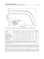
Fig. 16. Comparison of the gas sensitivity of three different morphologies of β-Ga
2
O
3
: (a)
single crystals, (b) bulk ceramics with closed pore structure, and (c) polycrystalline thin film
(Fleischer & Meixner, 1999)
However, sensitivities of three different morphologies of β-Ga
2
O
3
as single crystals, bulk
ceramics with closed pore structure and polycrystalline thin film were also investigated (see
Fig. 16) (Fleischer & Meixner, 1999).
Baban et al. proposed sandwich structure with double Ga
2
O
3
layer and mesh double Pt
electrode layer (Fig. 15. Type B), nevertheless, that device did not achieve neither higher
sensitivity nor fast response time, but it helped to conclude about the mechanism of
detection (Baban et al., 2005). The most commonly applied fabrication technique is
sputtering of thin Ga
2
O
3
and its subsequent annealing in order to achieve crystallization of
the layer. Although low-cost, screen printed, thick Ga
2
O
3
layers with sensing properties
similar to that based on thin layers could be also used (Frank a et al., 1998).
Sensing mechanism is assumed to be based on charge carrier exchange of adsorbed gas with
the surface of the sensing layer. Resistance modulation is a consequence of the change of
free charge carrier concentration resulted from the alteration of acceptor concentration on
the surface raising from the reaction of molecules with adsorbed oxygen ions when exposed
to oxygen containing ambient (Hoefer et al., 2001).
Generally adsorbed reducing or oxidizing gas species inject electrons into or extract
electrons from semiconducting material (Li et al., 2003) thus changing material conductivity.
Gallium oxide exhibits gas sensitivity at temperature range from 500 ºC to 1000 ºC. At lower
temperatures reducing gases sensitivity occurred. In the range from 900 ºC to 1000 ºC the
detection mechanism is bound to O
2
defects equilibrium in the lattice (Fleischer b et al.,
1996).
Modification of sensor parameters, such as sensitivity, selectivity (cross-sensitivity) and
response as well as recovery times for certain gas, could be assured by three ways:
temperature modulation, deposition of appropriate filter layer/clusters on the active layer
or by its doping. As described in (Fleischer a et al., 1995) gallium oxide layers of 2 μm
deposited by sputtering technique (grain sizes typically 50-100 nm) exhibited response to
reducing gases in the range of 500 – 650 ºC of operating temperatures. Increase of
temperature caused decrease of the sensitivity to these gases and simultaneous
enhancement of response to NH
4
. Temperatures of 740 – 780 ºC assured suppression of
reducing gases sensitivity leading to the selectivity to NH
4
.
Cross-sensitivity of ethanol and other organic solvents to methane were restricted by
application of filter layer of porous β-Ga
2
O
3
deposited on thin sensing Ga
2
O
3
layer Fig. 17
(Flingelli et al., 1998).
WetthermaloxidationofGaAsandGaN 123
presented better interface quality because less traps were formed at the interface between
GaN and the oxide due to more complete oxidation of GaN at higher temperature. But the
best current–voltage characteristics and C-V characteristics in accumulation region and
surface morphology had the sample from 800 °C oxidation process (Lin et al., 2006).
4.2 Gas sensors
Metal oxides Ga
2
O
3
gas sensors operating at high temperatures are an alternative for widely
used SnO
2
based sensors. Both types of sensors are not selective but react for a certain group
of gasses depending on the temperature of operation. Responses on oxygen, NO, CO, CH
4
,
H
2
, ethanol and acetone are most often investigated. Ga
2
O
3
sensors exhibit faster response
and recovery time, and lower cross-sensitivity to humidity than SnO
2
based sensors, see Fig.
14 (Fleischer & Meixner, 1999). Additional advantages are long-term stability and no
necessity of pre-ageing. Ga
2
O
3
sensors show stability in atmospheres with low oxygen
content what make them suitable for exhaust gas sensing. There is also no necessity of
degassing cycles in contrary to SnO
2
sensors. Disadvantages are lower sensitivity and higher
power consumption due to high temperature operation (Hoefer et al., 2001).
0.0 0.5 1.0 1.5 2.0
10
100
900
o
C
800
o
C
600
o
C
700
o
C
R [kOhm]
Humidity [%
abs
]
Fig. 14. Temperature dependence of the effect of humidity on the conductivity of Ga
2
O
3
thin
films, measured in synthetic air (Fleischer & Meixner, 1999)
Typical structure of a gas sensor consists of interdigital electrode (Fig. 16. Type A) (usually
platinum) deposited on the sensing layer composed of polycrystalline Ga
2
O
3
with grain
sizes of 10 and 50 nm (Fleischer a et al., 1996) or 50–100 nm (Schwebel et al., 2000; Fleischer
& Meixner et al., 1995).
Fig. 15. Typical interdigital oxide sensor (Type A) and modified mesh structure (Type B)
(Baban et al., 2005)
(a)
550 600 650 700 750 800 850 900
1
10
G
gas
/G
air
Temperature [
o
C]
O
2
1%
CH
4
0.5%
CO 0.5%
H
2
0.5%
(b)
550 600 650 700 750 800 850 900
0.7
0.8
0.9
1
2
G
gas
/G
air
Temperature [
o
C]
(c)
550 600 650 700 750 800 850 900
1
10
G
gas
/G
air
Temeperature [
o
C]
Fig. 16. Comparison of the gas sensitivity of three different morphologies of β-Ga
2
O
3
: (a)
single crystals, (b) bulk ceramics with closed pore structure, and (c) polycrystalline thin film
(Fleischer & Meixner, 1999)
However, sensitivities of three different morphologies of β-Ga
2
O
3
as single crystals, bulk
ceramics with closed pore structure and polycrystalline thin film were also investigated (see
Fig. 16) (Fleischer & Meixner, 1999).
Baban et al. proposed sandwich structure with double Ga
2
O
3
layer and mesh double Pt
electrode layer (Fig. 15. Type B), nevertheless, that device did not achieve neither higher
sensitivity nor fast response time, but it helped to conclude about the mechanism of
detection (Baban et al., 2005). The most commonly applied fabrication technique is
sputtering of thin Ga
2
O
3
and its subsequent annealing in order to achieve crystallization of
the layer. Although low-cost, screen printed, thick Ga
2
O
3
layers with sensing properties
similar to that based on thin layers could be also used (Frank a et al., 1998).
Sensing mechanism is assumed to be based on charge carrier exchange of adsorbed gas with
the surface of the sensing layer. Resistance modulation is a consequence of the change of
free charge carrier concentration resulted from the alteration of acceptor concentration on
the surface raising from the reaction of molecules with adsorbed oxygen ions when exposed
to oxygen containing ambient (Hoefer et al., 2001).
Generally adsorbed reducing or oxidizing gas species inject electrons into or extract
electrons from semiconducting material (Li et al., 2003) thus changing material conductivity.
Gallium oxide exhibits gas sensitivity at temperature range from 500 ºC to 1000 ºC. At lower
temperatures reducing gases sensitivity occurred. In the range from 900 ºC to 1000 ºC the
detection mechanism is bound to O
2
defects equilibrium in the lattice (Fleischer b et al.,
1996).
Modification of sensor parameters, such as sensitivity, selectivity (cross-sensitivity) and
response as well as recovery times for certain gas, could be assured by three ways:
temperature modulation, deposition of appropriate filter layer/clusters on the active layer
or by its doping. As described in (Fleischer a et al., 1995) gallium oxide layers of 2 μm
deposited by sputtering technique (grain sizes typically 50-100 nm) exhibited response to
reducing gases in the range of 500 – 650 ºC of operating temperatures. Increase of
temperature caused decrease of the sensitivity to these gases and simultaneous
enhancement of response to NH
4
. Temperatures of 740 – 780 ºC assured suppression of
reducing gases sensitivity leading to the selectivity to NH
4
.
Cross-sensitivity of ethanol and other organic solvents to methane were restricted by
application of filter layer of porous β-Ga
2
O
3
deposited on thin sensing Ga
2
O
3
layer Fig. 17
(Flingelli et al., 1998).
SemiconductorTechnologies124
60 90 120 150 180 210 240
0.1
1
10
100
Ga
2
O
3
-sensor-catalyst-device
Ga
2
O
3
-sensor
CO 3000 ppm
CO 6000 ppm
acetone 50 ppm
acetone 10 ppm
ethanol
300 ppm
ethanol 30 ppm
methane 500 ppm
methane 5000 ppm
R [kOhm]
t [min]
Fig. 17. Response of a pure Ga
2
O
3
sensor and a sensor catalyst device (hybrid research type)
to methane, ethanol, acetone and CO in wet synthetic air at 800 °C (Flingelli et al., 1998)
Fleischer et al. (Fleischer b et al., 1996) have investigated application of amorphous SiO
2
layer covering Ga
2
O
3
on the sensitivity, selectivity and stability of hydrogen sensor.
Polycrystalline, 2 μm thick gallium oxide layers were deposited by sputtering technique and
subsequently heated at 850 ºC for 15 hours or 1100 ºC for 1 hour. Crystallites sizes were 10
and 50 nm, respectively. Sensors sensitivity was investigated for: NO (300 ppm by vol.), CO
(100 ppm by vol.), CH
4
(1% by vol.), H
2
(1000 ppm by vol.), ethanol (15 ppm by vol.) and
acetone (15 ppm by vol.) In order to avoid cross-sensitivity the measurements were
prepared in 0.5% of humidity; also influence of humidity reduction to 0.025% by vol. as well
as O
2
content from 20 to 1% was evaluated. Uncoated Ga
2
O
3
sensor responded by decrease
of the conduction of the layer for reducing gases. At lower temperatures stronger response
was to more chemically reactive gases in contrary to higher temperatures where significant
response to chemically stable gasses was observed. Detection time of H
2
strongly depended
on the operating temperature of the sensor. Response time at 600 ºC was 10 min and 30 s at
above 700 ºC. Temperatures of 900 ºC and above assured rapid decrease in conductivity of
layer. All responses were reversible. To prevent the formation of oxygen on the Ga
2
O
3
surface during the oxidation process, what would exclude this kind of layers from the
application for H
2
sensing, additional SiO
2
layers were used. Use of 30 nm SiO
2
layer caused
lowering of response to reducing gases at temperatures of 900 ºC and below, except of H
2
.
The optimal operation temperature for H
2
detection was 800 ºC. Silicon dioxide layers of 300
nm thick have suppressed responses to all gasses at all temperatures except to H
2
. In this
case optimal temperature of operation was 700 ºC. Gallium oxide sensor with SiO
2
cap layer
could be used as a selective, high temperature hydrogen sensor (Fleischer b et al., 1996). To
assure of oxygen selectivity in oxygen-rich atmospheres Schwebel et al. (Schwebel et al.,
2000) have applied catalytically active oxides. Modification materials like CeO
2
, Mn
2
O
3
and
La
2
O
3
were deposited on the surface of 2 μm thick Ga
2
O
3
sputtered on ceramic substrates
and annealed at 1050 ºC for 10 hours (crystallite sizes 50–100 nm). Sensors with surface
modified by La
2
O
3
or CeO
2
responded only to oxygen changes in the ambient, in contrary to
uncoated Ga
2
O
3
sensor, which reacts with variety of gases. Modification of the surface with
Mn
2
O
3
caused insensitivity to any gases and thus could be used as reference sensor for
compensation of temperature influence in double sensor construction because of similar
values of thermal activation energy for conduction (Schwebel et al., 2000).
Gallium oxide sensors are sensitive for strongly reducing gases. Thus detection of NO
3
, NH
3
or CO
2
is considerably restricted. To investigate their influence on the selectivity various
layers like Ta
2
O
5
, WO
3
, NiO, AlVO
4
, SrTiO
2
, TiO
2
and Ta
2
O
3
were deposited on properly
prepared sensors consisting of 2 μm thick gallium oxide obtained by sputtering technique
and subsequently annealed. Application of TiO
2
and SrTiO
2
did not improve the selectivity
to O
2
or eliminate the cross-sensitivity to reducing gases. Modification of the surface with
WO
3
gave a strong reaction to NH
3
at 600 ºC and NO at 350 ºC compared to bare Ga
2
O
3
. In
case of NiO coating suppression of reaction with methane was revealed at 600-700 ºC. That
effect could be used as a reference in double sensor construction. Using of AlVO
4
assured
selectivity for O
2
when operating at 700 ºC and insensitivity to gases at temperature above
900 ºC (Fleischer a et al., 1996).
Lang et al. have applied modification of Ga
2
O
3
:SnO
2
sensing layer surface by iridium,
rhodium and ruthenium clusters. Ruthenium modified layers exhibited significant increase
of response on ethanol, when iridium modified sensor demonstrated enhanced sensitivity to
hydrogen at lower operating temperature. Sensitivity was 80 at 550 ºC (3000 ppm H
2
)
compared to unmodified sensor which sensitivity was 20 at 700 ºC (3000 ppm H
2
).
Measurements of as low concentration as 30 ppm were possible. Rhodium modified sensor
could be used only as a detector of presence of ethanol (Lang et al., 2000).
Dopants such as ZrO
2
, TiO
2
and MgO were applied in sandwich structure of sensor
containing as follows: substrate/Pt interdigital structure/Ga
2
O
3
/dopant/Ga
2
O
3
/dopant/
Ga
2
O
3
in order to investigate their influence on the sensitivity. However, no influence on the
sensitivity to O
2
was reported. Additionally, response decrease to CH
4
for ZrO
2
doping and
slight increase for MgO doping was observed (Frank et al., 1996).
Sensitivity to CO and CH
4
was achieved by application of SnO
2
doping in the sandwich
structure. The highest response was for 0.1% at. for both gases. However no influence of
doping on oxygen sensitivity was observed (Frank b et al., 1998).
Responses on oxygen of Ga
2
O
3
semiconducting thin films doped with Ce, Sb, W and Zn
were investigated by Li et al. 2003 (Li et al., 2003). Films doped with Zn exhibited the largest
responses for gas concentrations as follows: 100 ppm, 1000 ppm and 10000 ppm. The
optimum operation temperature was 420 ºC. On the other hand Ce doped gallium oxide
samples responded promptly to the gas induced. The reaction time was less than 40 s, when
that for Zn doped layer was 100 s. Baban et al. have obtained response times on oxygen of 14
and 27 s for ordinary interdigital platinum structure and newly proposed sandwich
structure, respectively (Baban et al., 2005). Li et al. have also investigated stability and
repeatability of the sensors. Responses of all sensors were relatively reproducible, see Fig. 18
(Li et al., 2003).
WetthermaloxidationofGaAsandGaN 125
60 90 120 150 180 210 240
0.1
1
10
100
Ga
2
O
3
-sensor-catalyst-device
Ga
2
O
3
-sensor
CO 3000 ppm
CO 6000 ppm
acetone 50 ppm
acetone 10 ppm
ethanol
300 ppm
ethanol 30 ppm
methane 500 ppm
methane 5000 ppm
R [kOhm]
t [min]
Fig. 17. Response of a pure Ga
2
O
3
sensor and a sensor catalyst device (hybrid research type)
to methane, ethanol, acetone and CO in wet synthetic air at 800 °C (Flingelli et al., 1998)
Fleischer et al. (Fleischer b et al., 1996) have investigated application of amorphous SiO
2
layer covering Ga
2
O
3
on the sensitivity, selectivity and stability of hydrogen sensor.
Polycrystalline, 2 μm thick gallium oxide layers were deposited by sputtering technique and
subsequently heated at 850 ºC for 15 hours or 1100 ºC for 1 hour. Crystallites sizes were 10
and 50 nm, respectively. Sensors sensitivity was investigated for: NO (300 ppm by vol.), CO
(100 ppm by vol.), CH
4
(1% by vol.), H
2
(1000 ppm by vol.), ethanol (15 ppm by vol.) and
acetone (15 ppm by vol.) In order to avoid cross-sensitivity the measurements were
prepared in 0.5% of humidity; also influence of humidity reduction to 0.025% by vol. as well
as O
2
content from 20 to 1% was evaluated. Uncoated Ga
2
O
3
sensor responded by decrease
of the conduction of the layer for reducing gases. At lower temperatures stronger response
was to more chemically reactive gases in contrary to higher temperatures where significant
response to chemically stable gasses was observed. Detection time of H
2
strongly depended
on the operating temperature of the sensor. Response time at 600 ºC was 10 min and 30 s at
above 700 ºC. Temperatures of 900 ºC and above assured rapid decrease in conductivity of
layer. All responses were reversible. To prevent the formation of oxygen on the Ga
2
O
3
surface during the oxidation process, what would exclude this kind of layers from the
application for H
2
sensing, additional SiO
2
layers were used. Use of 30 nm SiO
2
layer caused
lowering of response to reducing gases at temperatures of 900 ºC and below, except of H
2
.
The optimal operation temperature for H
2
detection was 800 ºC. Silicon dioxide layers of 300
nm thick have suppressed responses to all gasses at all temperatures except to H
2
. In this
case optimal temperature of operation was 700 ºC. Gallium oxide sensor with SiO
2
cap layer
could be used as a selective, high temperature hydrogen sensor (Fleischer b et al., 1996). To
assure of oxygen selectivity in oxygen-rich atmospheres Schwebel et al. (Schwebel et al.,
2000) have applied catalytically active oxides. Modification materials like CeO
2
, Mn
2
O
3
and
La
2
O
3
were deposited on the surface of 2 μm thick Ga
2
O
3
sputtered on ceramic substrates
and annealed at 1050 ºC for 10 hours (crystallite sizes 50–100 nm). Sensors with surface
modified by La
2
O
3
or CeO
2
responded only to oxygen changes in the ambient, in contrary to
uncoated Ga
2
O
3
sensor, which reacts with variety of gases. Modification of the surface with
Mn
2
O
3
caused insensitivity to any gases and thus could be used as reference sensor for
compensation of temperature influence in double sensor construction because of similar
values of thermal activation energy for conduction (Schwebel et al., 2000).
Gallium oxide sensors are sensitive for strongly reducing gases. Thus detection of NO
3
, NH
3
or CO
2
is considerably restricted. To investigate their influence on the selectivity various
layers like Ta
2
O
5
, WO
3
, NiO, AlVO
4
, SrTiO
2
, TiO
2
and Ta
2
O
3
were deposited on properly
prepared sensors consisting of 2 μm thick gallium oxide obtained by sputtering technique
and subsequently annealed. Application of TiO
2
and SrTiO
2
did not improve the selectivity
to O
2
or eliminate the cross-sensitivity to reducing gases. Modification of the surface with
WO
3
gave a strong reaction to NH
3
at 600 ºC and NO at 350 ºC compared to bare Ga
2
O
3
. In
case of NiO coating suppression of reaction with methane was revealed at 600-700 ºC. That
effect could be used as a reference in double sensor construction. Using of AlVO
4
assured
selectivity for O
2
when operating at 700 ºC and insensitivity to gases at temperature above
900 ºC (Fleischer a et al., 1996).
Lang et al. have applied modification of Ga
2
O
3
:SnO
2
sensing layer surface by iridium,
rhodium and ruthenium clusters. Ruthenium modified layers exhibited significant increase
of response on ethanol, when iridium modified sensor demonstrated enhanced sensitivity to
hydrogen at lower operating temperature. Sensitivity was 80 at 550 ºC (3000 ppm H
2
)
compared to unmodified sensor which sensitivity was 20 at 700 ºC (3000 ppm H
2
).
Measurements of as low concentration as 30 ppm were possible. Rhodium modified sensor
could be used only as a detector of presence of ethanol (Lang et al., 2000).
Dopants such as ZrO
2
, TiO
2
and MgO were applied in sandwich structure of sensor
containing as follows: substrate/Pt interdigital structure/Ga
2
O
3
/dopant/Ga
2
O
3
/dopant/
Ga
2
O
3
in order to investigate their influence on the sensitivity. However, no influence on the
sensitivity to O
2
was reported. Additionally, response decrease to CH
4
for ZrO
2
doping and
slight increase for MgO doping was observed (Frank et al., 1996).
Sensitivity to CO and CH
4
was achieved by application of SnO
2
doping in the sandwich
structure. The highest response was for 0.1% at. for both gases. However no influence of
doping on oxygen sensitivity was observed (Frank b et al., 1998).
Responses on oxygen of Ga
2
O
3
semiconducting thin films doped with Ce, Sb, W and Zn
were investigated by Li et al. 2003 (Li et al., 2003). Films doped with Zn exhibited the largest
responses for gas concentrations as follows: 100 ppm, 1000 ppm and 10000 ppm. The
optimum operation temperature was 420 ºC. On the other hand Ce doped gallium oxide
samples responded promptly to the gas induced. The reaction time was less than 40 s, when
that for Zn doped layer was 100 s. Baban et al. have obtained response times on oxygen of 14
and 27 s for ordinary interdigital platinum structure and newly proposed sandwich
structure, respectively (Baban et al., 2005). Li et al. have also investigated stability and
repeatability of the sensors. Responses of all sensors were relatively reproducible, see Fig. 18
(Li et al., 2003).
SemiconductorTechnologies126
Fig. 18. Electrical response of doped Ga
2
O
3
films at temperature of 500 ºC (1000 ppm O
2
) (Li
et al., 2003)
Sensors doped with Sb and W after exposure to the analyzed gas exhibited initial growth of
resistance followed by its exponential decrease.
5. Conclusion
Gallium oxide appeared to be a good candidate for optoelectronic and electronic
applications. Intrinsic Ga
2
O
3
layers have insulating nature, but after appropriate
modification could reach conductive parameters. Very interesting effect is n-type
semiconducting behavior at elevated temperatures originating from oxygen deficiencies in
Ga
2
O
3
. Gallium oxide is a material included to the group of transparent conductive oxides
(TCOs) that are of great interest. Among all TCOs, e.g. ITO or ZnO, β-Ga
2
O
3
has the largest
value of band-gap what assures high transparency in the range from visible to deep-UV
wavelengths. Additionally β-Ga
2
O
3
is chemically and thermally stable. That all advantages
make β-Ga
2
O
3
to be intensively investigated although there is a lot of issues that should
researched.
In the chapter main focus was placed on the monoclinic gallium oxide and its most widely
applied fabrication methods. There is also a large part devoted to the application of that
material. Metal Oxide Semiconductor transistors and gas sensors, based on pure and doped
gallium oxide, principles of operation and parameters were described.
Parameters of Ga
2
O
3
chosen to the analysis and discussion were selected concerning
possible application of that material. Influence of parameters of process of layers deposition
or crystal growth on the electrical as well as optical parameters of gallium oxide was
included. Possible ways of modification of layers properties are also embraced.
6. Refereces
Al-Kuhaili, M.F.; Durrani, S.M.A. & Khawaja, E.E. (2003). Optical properties of gallium
oxide films deposited by electron beam evaporation. Applied Physics Letters, Vol. 83,
No. 22, (December 2003) 4533-4535, ISSN: 0003-6951
Baban, C.; Toyoda, Y. & Ogita, M. (2005). Oxygen sensing at high temperatures using Ga
2
O
3
films. Thin Solid Films, Vol. 484, No. 1-2, (July 2005) 369-373, ISSN: 0040-6090
Battiston, G.A.; Gerbasi, R.; Porchia, M.; Bertoncello, R. & Caccavale, F. (1996). Chemical
vapour deposition and characterization of gallium oxide thin films. Thin Solid
Films, Vol. 279, No. 1-2, (June 1996) 115-118, ISSN: 0040-6090
Bermudez, V. M. (1983). Photoenhanced oxidation of gallium arsenide. Journal of Applied
Physics, Vol. 54, No. 11, (November 1983) 6795-6798, ISSN: 0021-8979
Chen, P.; Zhang R.; Xu X.F.; Chen Z.Z.; Zhou Y.G.; Xie S.Y.; Shi Y.; Shen B.; Gu S.L.;
Huang Z.C.; Hu J. & Zheng Y.D. (2000). Oxidation of gallium nitride epilayers
in dry oxygen. Journal of Applied Physics A: Materials Science & Processing, Vol.
71, No. 2, (August 2000) 191-194, ISSN: 09478396
Choe, J S.; Park S H.; Choe B D. & Jeon H. (2000). Lateral oxidation of AlAs layers at
elevated water vapour pressure using a closed-chamber system. Semiconductor
Science and Technology, Vol. 15, No. 10, (October 2000) L35-L38, ISSN: 0268-1242
Fleischer, M. & Meixner, H. (1993). Electron mobility in single- and polycrystalline
Ga
2
O
3
. Journal of Applied Physics, Vol. 74, No. 1, (July 1993) 300-305,
ISSN: 0021-8979
Fleischer, M. & Meixner, H. (1995). Sensitive, selective and stable CH
4
detection using
semiconducting Ga
2
O
3
thin films. Sensors and Actuators B, Vol. 26, No. 1, (May
1995) 81-84, ISSN: 0925-4005
Fleischer a, M.; Seth, M.; Kohl, C D. & Meixner, H. (1996). A study of surface
modification at semiconducting Ga
2
O
3
thin film sensors for enhancement of the
sensitivity and selectivity. Sensors and Actuators B, Vol. 35-36, No. 1-3, (October
1996) 290-296, ISSN: 0925-4005
Fleischer b, M.; Seth, M.; Kohl, C D. & Meixner, H. (1996). A selective H
2
sensor
implemented using Ga
2
O
3
thin-films which were covered with a gas filtering
SiO
2
layer. Sensors and Actuators B, Vol. 35-36, No. 1-3, (October 1996) 297-302,
ISSN: 0925-4005
Fleischer, M. & Meixner, H. (1999). Thin-film gas sensors based on high-temperature-
operated metal oxides. Journal of Vacuum Science and Technology A, Vol. 14, No.
4, (July/August 1999) 1866-1872, ISSN: 0734-2101
Flingelli, G.K.; Fleischer, M.M. & Meixner, H. (1998). Selective detection of methane in
domestic environments using a catalyst sensor system based on Ga
2
O
3
. Sensors
and Actuators B, Vol. 48, No. 1, (May 1998) 258-262, ISSN: 0925-4005
Frank, J.; Fleischer, M. & Meixner, H. (1996). Electrical doping of gas-sensitive,
semiconducting Ga
2
O
3
thin films. Sensors and Actuators B, Vol. 34, No. 1,
(August 1996) 373-377, ISSN: 0925-4005
Frank a, J.; Fleischer, M. & Meixner, H. (1998). Gas-sensitive electrical properties of pure
and doped semiconducting Ga
2
O
3
thick films. Sensors and Actuators B, Vol. 48,
No. 1, (May 1998) 318-321, ISSN: 0925-4005
Frank b, J.; Fleischer, M.; Meixner, H.; & Feltz, A. (1998). Enhancement of sensitivity
and conductivity of semiconducting Ga
2
O
3
gas sensors by doping with SnO
2
.
Sensors and Actuators B, Vol. 49, No. 1, (June 1998) 110-114, ISSN: 0925-4005
Ghidaoui, D.; Lyon, S. B.; Thomson, G. E. & Walton, J. (2002). Oxide formation during
etching of gallium arsenide. Corrosion Science, Vol. 44, No. 3, (March 2002) 501-
509, ISSN: 0010-938X
WetthermaloxidationofGaAsandGaN 127
Fig. 18. Electrical response of doped Ga
2
O
3
films at temperature of 500 ºC (1000 ppm O
2
) (Li
et al., 2003)
Sensors doped with Sb and W after exposure to the analyzed gas exhibited initial growth of
resistance followed by its exponential decrease.
5. Conclusion
Gallium oxide appeared to be a good candidate for optoelectronic and electronic
applications. Intrinsic Ga
2
O
3
layers have insulating nature, but after appropriate
modification could reach conductive parameters. Very interesting effect is n-type
semiconducting behavior at elevated temperatures originating from oxygen deficiencies in
Ga
2
O
3
. Gallium oxide is a material included to the group of transparent conductive oxides
(TCOs) that are of great interest. Among all TCOs, e.g. ITO or ZnO, β-Ga
2
O
3
has the largest
value of band-gap what assures high transparency in the range from visible to deep-UV
wavelengths. Additionally β-Ga
2
O
3
is chemically and thermally stable. That all advantages
make β-Ga
2
O
3
to be intensively investigated although there is a lot of issues that should
researched.
In the chapter main focus was placed on the monoclinic gallium oxide and its most widely
applied fabrication methods. There is also a large part devoted to the application of that
material. Metal Oxide Semiconductor transistors and gas sensors, based on pure and doped
gallium oxide, principles of operation and parameters were described.
Parameters of Ga
2
O
3
chosen to the analysis and discussion were selected concerning
possible application of that material. Influence of parameters of process of layers deposition
or crystal growth on the electrical as well as optical parameters of gallium oxide was
included. Possible ways of modification of layers properties are also embraced.
6. Refereces
Al-Kuhaili, M.F.; Durrani, S.M.A. & Khawaja, E.E. (2003). Optical properties of gallium
oxide films deposited by electron beam evaporation. Applied Physics Letters, Vol. 83,
No. 22, (December 2003) 4533-4535, ISSN: 0003-6951
Baban, C.; Toyoda, Y. & Ogita, M. (2005). Oxygen sensing at high temperatures using Ga
2
O
3
films. Thin Solid Films, Vol. 484, No. 1-2, (July 2005) 369-373, ISSN: 0040-6090
Battiston, G.A.; Gerbasi, R.; Porchia, M.; Bertoncello, R. & Caccavale, F. (1996). Chemical
vapour deposition and characterization of gallium oxide thin films. Thin Solid
Films, Vol. 279, No. 1-2, (June 1996) 115-118, ISSN: 0040-6090
Bermudez, V. M. (1983). Photoenhanced oxidation of gallium arsenide. Journal of Applied
Physics, Vol. 54, No. 11, (November 1983) 6795-6798, ISSN: 0021-8979
Chen, P.; Zhang R.; Xu X.F.; Chen Z.Z.; Zhou Y.G.; Xie S.Y.; Shi Y.; Shen B.; Gu S.L.;
Huang Z.C.; Hu J. & Zheng Y.D. (2000). Oxidation of gallium nitride epilayers
in dry oxygen. Journal of Applied Physics A: Materials Science & Processing, Vol.
71, No. 2, (August 2000) 191-194, ISSN: 09478396
Choe, J S.; Park S H.; Choe B D. & Jeon H. (2000). Lateral oxidation of AlAs layers at
elevated water vapour pressure using a closed-chamber system. Semiconductor
Science and Technology, Vol. 15, No. 10, (October 2000) L35-L38, ISSN: 0268-1242
Fleischer, M. & Meixner, H. (1993). Electron mobility in single- and polycrystalline
Ga
2
O
3
. Journal of Applied Physics, Vol. 74, No. 1, (July 1993) 300-305,
ISSN: 0021-8979
Fleischer, M. & Meixner, H. (1995). Sensitive, selective and stable CH
4
detection using
semiconducting Ga
2
O
3
thin films. Sensors and Actuators B, Vol. 26, No. 1, (May
1995) 81-84, ISSN: 0925-4005
Fleischer a, M.; Seth, M.; Kohl, C D. & Meixner, H. (1996). A study of surface
modification at semiconducting Ga
2
O
3
thin film sensors for enhancement of the
sensitivity and selectivity. Sensors and Actuators B, Vol. 35-36, No. 1-3, (October
1996) 290-296, ISSN: 0925-4005
Fleischer b, M.; Seth, M.; Kohl, C D. & Meixner, H. (1996). A selective H
2
sensor
implemented using Ga
2
O
3
thin-films which were covered with a gas filtering
SiO
2
layer. Sensors and Actuators B, Vol. 35-36, No. 1-3, (October 1996) 297-302,
ISSN: 0925-4005
Fleischer, M. & Meixner, H. (1999). Thin-film gas sensors based on high-temperature-
operated metal oxides. Journal of Vacuum Science and Technology A, Vol. 14, No.
4, (July/August 1999) 1866-1872, ISSN: 0734-2101
Flingelli, G.K.; Fleischer, M.M. & Meixner, H. (1998). Selective detection of methane in
domestic environments using a catalyst sensor system based on Ga
2
O
3
. Sensors
and Actuators B, Vol. 48, No. 1, (May 1998) 258-262, ISSN: 0925-4005
Frank, J.; Fleischer, M. & Meixner, H. (1996). Electrical doping of gas-sensitive,
semiconducting Ga
2
O
3
thin films. Sensors and Actuators B, Vol. 34, No. 1,
(August 1996) 373-377, ISSN: 0925-4005
Frank a, J.; Fleischer, M. & Meixner, H. (1998). Gas-sensitive electrical properties of pure
and doped semiconducting Ga
2
O
3
thick films. Sensors and Actuators B, Vol. 48,
No. 1, (May 1998) 318-321, ISSN: 0925-4005
Frank b, J.; Fleischer, M.; Meixner, H.; & Feltz, A. (1998). Enhancement of sensitivity
and conductivity of semiconducting Ga
2
O
3
gas sensors by doping with SnO
2
.
Sensors and Actuators B, Vol. 49, No. 1, (June 1998) 110-114, ISSN: 0925-4005
Ghidaoui, D.; Lyon, S. B.; Thomson, G. E. & Walton, J. (2002). Oxide formation during
etching of gallium arsenide. Corrosion Science, Vol. 44, No. 3, (March 2002) 501-
509, ISSN: 0010-938X
SemiconductorTechnologies128
Gila, B. P.; Lee, K. N.; Johnson, W.; Ren, F.; Abernathy, C. R.; Pearton, S. J.; Hong, M.;
Kwo, J.; Mannaerts, J. P.; Anselm, K. A. (2000). A comparison of gallium
gadolinium oxide and gadolinium oxide for use as dielectrics in GaN
MOSFETs; High Performance Devices, Proceedings of IEEE/Cornell Conference 2000,
pp. 182-191, August 2000, Ithaca, NY, USA, ISBN: 0-7803-6381-7, IEEE CNF
Hao, J. & Cocivera, M. (2002). Optical and luminescent properties of undoped and rare-
earth-doped Ga
2
O
3
thin films deposited by spray pyrolysis. Journal of Physics D:
Applied Physics, Vol. 35, No. 5, (March 2002) 433-438, ISSN: 0022-3727
Hoefer, U.; Franf, J. & Fleischer, M. (2001). High temperature Ga
2
O
3
-gas sensors and
SnO
2
-gas sensors: a comparison. Sensors and Actuators B, Vol. 78, No. 1, (August
2001) 6-11, ISSN: 0925-4005
Hong, M.; Lee, W. C.; Huang, M. L.; Chang, Y. C.; Lin, T. D.; Lee, Y. J.; Kwo, J.; Hsu, C.
H. & Lee, H. Y. (2007). Defining new frontiers in electronic devices with high
kappa dielectrics and interfacial engineering. Thin Solid Films, Vol. 515, No. 14,
(May 2007) 5581-5586, ISSN: 0040-6090
Jing, Z.; Kosel, T. H.; Hall, D. C. & Fay, P. (2008). Fabrication and Performance of 0.25-
µm Gate Length Depletion-Mode GaAs-Channel MOSFETs With Self-Aligned
InAlP Native Oxide Gate Dielectric. Electron Device Letters, IEEE, Vol. 29, No. 2,
(February 2008) 143-145, ISSN: 0741-3106
Jun, B. K.; Kim D.;H.; Leem, J. Y.; Lee, J. H.; Lee, Y. H. (2000), Fabrication of a depletion
mode GaAs MOSFET using Al
2
O
3
as a gate insulator through the selective wet
oxidation of AlAs, Thin Solid Films, Vol. 360, No. 1-2, (February 2000), 229-232,
ISSN: 0040-6090
Kasu, M. (2004), Selected Papers: Advanced Materials and Their Applications to Future
Functional Devices - Microwave Operation of Diamond Field-Effect Transistor,
NTT Technical Review, Vol. 2, No. 6, (June 2004), 19-24, ISSN: 13483447
Kim, H-G. & Kim, W-T. (2000). Optical properties of β-Ga
2
O
3
and α-Ga
2
O
3
:Co thin films
grown by spray pyrolysis, Journal of Applied Physics, Vol. 62, No. 5, (September
1987) 2000-2002, ISSN: 0021-8979
Kim, H.; Park, S J. & Hwang, H. (2001). Thermally oxidized GaN film for use as gate
insulators. Journal of Vacuum Science & Technology B, Vol. 19, No. 2.,
(March/April 2001) 579-581, ISSN: 1071-1023
Kim, H.W. & Kim, N.H. (2004). Annealing effects on the properties of Ga
a
O
3
thin films
grown on sapphire substrates by metal organic chemical vapor deposition.
Applied Surface Science, Vol. 230, No. 1-4, (May 2004) 301-306, ISSN: 0169-4332
Korbutowicz, R.; Prażmowska, J.; Wągrowski, Z.; Szyszka, A. & Tłaczała, M. (2008), Wet
thermal oxidation for GaAs, GaN and Metal/GaN device applications, The
Seventh International Conference on Advanced Semiconductor Devices and
Microsystems. ASDAM 2008, pp. 163-166, ISBN: 978-1-4244-2325-5, Smolenice,
Slovakia, October 2008, Ed. by S. Hašcik, J. Osvald, NJ: IEEE CNF, cop. 2008,
Piscataway
Lang, A.C.; Fleischer, M. & Meixner, H. (2000). Surface modifications of Ga
2
O
3
thin film
sensors with Rh, Ru and Ir clusters. Sensors and Actuators B, Vol. 66, No. 1, (July
2000) 80-84, ISSN: 0925-4005
Lazzarino, M.; Padovani, M.; Mori, G.; Sorba, L.; Fanetti, M. & Sancrotti, M. (2005).
Chemical composition of GaAs oxides grown by local anodic oxidation: a
spatially resolved Auger study. Chemical Physics Letters, Vol. 402, No. 1-3,
(January 2005) 155-159, ISSN: 0009-2614
Lazzarino, M.; Mori, G.; Sorba, L.; Ercolani, D.; Biasiol, G.; Heun, S. & Locatelli, A.
(2006). Chemistry and formation process of Ga(Al)As oxide during local anodic
oxidation nanolithography. Surface Science, Vol. 600, No. 18, (September 2006),
3739-3743, ISSN: 0039-6028
Li, Y.; Trinchi, A.; Włodarski, W.; Galatsis, K. & Kalantar-zadeh, K. (2003). Investigation
of the oxygen gas sensing performance of Ga
2
O
3
thin films with different
dopants, Sensors and Actuators B, Vol. 93, No. 1 , (August 2003) 431 – 434, ISSN:
0925-4005
Lin, L.; Luo, Y.; Lai, P.T. & Lau, K. M. (2005). Effects of oxidation temperature on Ga
2
O
3
film thermally grown on GaN, Proceedings of 2005 IEEE Conference on Electron
Devices and Solid-State Circuits, pp. 605-608, ISBN: 0-7803-9339-2, Hong Kong,
December 2005
Lin, L. M.; Luo, Y.; Lai, P. T. & Lau, K. M. (2006). Influence of oxidation and annealing
temperatures on quality of Ga
2
O
3
film grown on GaN. Thin Solid Films, Vol.
515, No. 4, (December 2006) 2111-2115, ISSN: 0040-6090
Martens, K.; Wang, W.F.; Dimoulas, A.; Borghs, G.; Meuris, M.; Groeseneken, G. &
Maes, H.,E. (2007). Determining weak Fermi-level pinning in MOS devices by
conductance and capacitance analysis and application to GaAs MOS devices.
Solid-State Electronics, Vol. 51, No. 8, (August 2007) 1101–1108, ISSN: 0038-1101
Matsuzaki, Y.; Hamada, A. & Konagai, M. (2000). Improvement of nanoscale patterning
of heavily doped p-type GaAs by atomic force microscope (AFM)-based surface
oxidation process. Journal of Crystal Growth, Vol. 209, No. 2-3, (February 2000)
509-512, ISSN: 0022-0248
Matsuzaki, K.; Hiramatsu, H.; Nomra, K.; Yanagi, H.; Kamiya, T.; Hirano, M. & Holono,
H. (2006). Growth structure, and carrier transport properties of Ga
2
O
3
epitaxial
film examined for transparent field-effect transistor. Thin Solid Films, Vol. 496,
No. 1, (February 2006) 37-41, ISSN: 0040-6090
Nakano, Y. & Jimbo, T. (2003). Interface properties of thermally oxidized n-GaN metal–
oxide–semiconductor capacitors. Applied Physics Letters, Vol. 82, No. 2, (January
2003) 218-220, ISSN: 0003-6951
Nakano a, Y.; Kachi, T. & Jimbo, T. (2003). Electrical properties of thermally oxidized p-
GaN metal–oxide–semiconductor diodes. Applied Physics Letters, Vol. 82, No. 15,
(April 2003) 2443-2245, ISSN: 0003-6951
Nakano b, Y.; Kachi, T. & Jimbo, T. (2003). Inversion behavior in thermally oxidized p-
GaN metal–oxide–semiconductor capacitors. Journal of Vacuum Science and
Technology B, Vol. 21, No. 5 (September/October2003) 2220-2222, ISSN: 1071-
1023
Offsey, S. D.; Woodall, J. M., Warren, A. C.; Kirchner, P. D.; Chappell, T. I. & Pettit, G.
D. (1986). Unpinned (100) GaAs surfaces in air using photochemistry. Applied
Physics Letters, Vol. 48, No. 7, (February 1986) 475-477, ISSN: 0003-6951
WetthermaloxidationofGaAsandGaN 129
Gila, B. P.; Lee, K. N.; Johnson, W.; Ren, F.; Abernathy, C. R.; Pearton, S. J.; Hong, M.;
Kwo, J.; Mannaerts, J. P.; Anselm, K. A. (2000). A comparison of gallium
gadolinium oxide and gadolinium oxide for use as dielectrics in GaN
MOSFETs; High Performance Devices, Proceedings of IEEE/Cornell Conference 2000,
pp. 182-191, August 2000, Ithaca, NY, USA, ISBN: 0-7803-6381-7, IEEE CNF
Hao, J. & Cocivera, M. (2002). Optical and luminescent properties of undoped and rare-
earth-doped Ga
2
O
3
thin films deposited by spray pyrolysis. Journal of Physics D:
Applied Physics, Vol. 35, No. 5, (March 2002) 433-438, ISSN: 0022-3727
Hoefer, U.; Franf, J. & Fleischer, M. (2001). High temperature Ga
2
O
3
-gas sensors and
SnO
2
-gas sensors: a comparison. Sensors and Actuators B, Vol. 78, No. 1, (August
2001) 6-11, ISSN: 0925-4005
Hong, M.; Lee, W. C.; Huang, M. L.; Chang, Y. C.; Lin, T. D.; Lee, Y. J.; Kwo, J.; Hsu, C.
H. & Lee, H. Y. (2007). Defining new frontiers in electronic devices with high
kappa dielectrics and interfacial engineering. Thin Solid Films, Vol. 515, No. 14,
(May 2007) 5581-5586, ISSN: 0040-6090
Jing, Z.; Kosel, T. H.; Hall, D. C. & Fay, P. (2008). Fabrication and Performance of 0.25-
µm Gate Length Depletion-Mode GaAs-Channel MOSFETs With Self-Aligned
InAlP Native Oxide Gate Dielectric. Electron Device Letters, IEEE, Vol. 29, No. 2,
(February 2008) 143-145, ISSN: 0741-3106
Jun, B. K.; Kim D.;H.; Leem, J. Y.; Lee, J. H.; Lee, Y. H. (2000), Fabrication of a depletion
mode GaAs MOSFET using Al
2
O
3
as a gate insulator through the selective wet
oxidation of AlAs, Thin Solid Films, Vol. 360, No. 1-2, (February 2000), 229-232,
ISSN: 0040-6090
Kasu, M. (2004), Selected Papers: Advanced Materials and Their Applications to Future
Functional Devices - Microwave Operation of Diamond Field-Effect Transistor,
NTT Technical Review, Vol. 2, No. 6, (June 2004), 19-24, ISSN: 13483447
Kim, H-G. & Kim, W-T. (2000). Optical properties of β-Ga
2
O
3
and α-Ga
2
O
3
:Co thin films
grown by spray pyrolysis, Journal of Applied Physics, Vol. 62, No. 5, (September
1987) 2000-2002, ISSN: 0021-8979
Kim, H.; Park, S J. & Hwang, H. (2001). Thermally oxidized GaN film for use as gate
insulators. Journal of Vacuum Science & Technology B, Vol. 19, No. 2.,
(March/April 2001) 579-581, ISSN: 1071-1023
Kim, H.W. & Kim, N.H. (2004). Annealing effects on the properties of Ga
a
O
3
thin films
grown on sapphire substrates by metal organic chemical vapor deposition.
Applied Surface Science, Vol. 230, No. 1-4, (May 2004) 301-306, ISSN: 0169-4332
Korbutowicz, R.; Prażmowska, J.; Wągrowski, Z.; Szyszka, A. & Tłaczała, M. (2008), Wet
thermal oxidation for GaAs, GaN and Metal/GaN device applications, The
Seventh International Conference on Advanced Semiconductor Devices and
Microsystems. ASDAM 2008, pp. 163-166, ISBN: 978-1-4244-2325-5, Smolenice,
Slovakia, October 2008, Ed. by S. Hašcik, J. Osvald, NJ: IEEE CNF, cop. 2008,
Piscataway
Lang, A.C.; Fleischer, M. & Meixner, H. (2000). Surface modifications of Ga
2
O
3
thin film
sensors with Rh, Ru and Ir clusters. Sensors and Actuators B, Vol. 66, No. 1, (July
2000) 80-84, ISSN: 0925-4005
Lazzarino, M.; Padovani, M.; Mori, G.; Sorba, L.; Fanetti, M. & Sancrotti, M. (2005).
Chemical composition of GaAs oxides grown by local anodic oxidation: a
spatially resolved Auger study. Chemical Physics Letters, Vol. 402, No. 1-3,
(January 2005) 155-159, ISSN: 0009-2614
Lazzarino, M.; Mori, G.; Sorba, L.; Ercolani, D.; Biasiol, G.; Heun, S. & Locatelli, A.
(2006). Chemistry and formation process of Ga(Al)As oxide during local anodic
oxidation nanolithography. Surface Science, Vol. 600, No. 18, (September 2006),
3739-3743, ISSN: 0039-6028
Li, Y.; Trinchi, A.; Włodarski, W.; Galatsis, K. & Kalantar-zadeh, K. (2003). Investigation
of the oxygen gas sensing performance of Ga
2
O
3
thin films with different
dopants, Sensors and Actuators B, Vol. 93, No. 1 , (August 2003) 431 – 434, ISSN:
0925-4005
Lin, L.; Luo, Y.; Lai, P.T. & Lau, K. M. (2005). Effects of oxidation temperature on Ga
2
O
3
film thermally grown on GaN, Proceedings of 2005 IEEE Conference on Electron
Devices and Solid-State Circuits, pp. 605-608, ISBN: 0-7803-9339-2, Hong Kong,
December 2005
Lin, L. M.; Luo, Y.; Lai, P. T. & Lau, K. M. (2006). Influence of oxidation and annealing
temperatures on quality of Ga
2
O
3
film grown on GaN. Thin Solid Films, Vol.
515, No. 4, (December 2006) 2111-2115, ISSN: 0040-6090
Martens, K.; Wang, W.F.; Dimoulas, A.; Borghs, G.; Meuris, M.; Groeseneken, G. &
Maes, H.,E. (2007). Determining weak Fermi-level pinning in MOS devices by
conductance and capacitance analysis and application to GaAs MOS devices.
Solid-State Electronics, Vol. 51, No. 8, (August 2007) 1101–1108, ISSN: 0038-1101
Matsuzaki, Y.; Hamada, A. & Konagai, M. (2000). Improvement of nanoscale patterning
of heavily doped p-type GaAs by atomic force microscope (AFM)-based surface
oxidation process. Journal of Crystal Growth, Vol. 209, No. 2-3, (February 2000)
509-512, ISSN: 0022-0248
Matsuzaki, K.; Hiramatsu, H.; Nomra, K.; Yanagi, H.; Kamiya, T.; Hirano, M. & Holono,
H. (2006). Growth structure, and carrier transport properties of Ga
2
O
3
epitaxial
film examined for transparent field-effect transistor. Thin Solid Films, Vol. 496,
No. 1, (February 2006) 37-41, ISSN: 0040-6090
Nakano, Y. & Jimbo, T. (2003). Interface properties of thermally oxidized n-GaN metal–
oxide–semiconductor capacitors. Applied Physics Letters, Vol. 82, No. 2, (January
2003) 218-220, ISSN: 0003-6951
Nakano a, Y.; Kachi, T. & Jimbo, T. (2003). Electrical properties of thermally oxidized p-
GaN metal–oxide–semiconductor diodes. Applied Physics Letters, Vol. 82, No. 15,
(April 2003) 2443-2245, ISSN: 0003-6951
Nakano b, Y.; Kachi, T. & Jimbo, T. (2003). Inversion behavior in thermally oxidized p-
GaN metal–oxide–semiconductor capacitors. Journal of Vacuum Science and
Technology B, Vol. 21, No. 5 (September/October2003) 2220-2222, ISSN: 1071-
1023
Offsey, S. D.; Woodall, J. M., Warren, A. C.; Kirchner, P. D.; Chappell, T. I. & Pettit, G.
D. (1986). Unpinned (100) GaAs surfaces in air using photochemistry. Applied
Physics Letters, Vol. 48, No. 7, (February 1986) 475-477, ISSN: 0003-6951
SemiconductorTechnologies130
Orita, M.; Ohta, H.; Hirano, M. & Hosono, H. (2000). Deep-ultraviolet transparent
conductive -Ga
2
O
3
thin films. Applied Physics Letters, Vol. 77, No. 25,
(December 2000) 4166-4168, ISSN: 0003-6951
Orita, M.; Hiramatsu, H.; Ohta, H.; Hirano, M. & Hosono H. (2002). Preparation of
highly conductive, deep ultraviolet transparent -Ga
2
O
3
thin film at low
deposition temperatures. Thin Solid Films, Vol. 411, No. 1, (May 2002) 134–139,
ISSN: 0040-6090
Oshima, T.; Okuno, T. & Fujita, S. (2007). Ga
2
O
3
Thin Film Growth on c-Plane Sapphire
Substrates by Molecular Beam Epitaxy for Deep-Ultraviolet Photodetectors.
Japanese Journal of Applied Physics, Vol. 46, No. 11, (November 2007) 7217-7220,
ISSN: 1347-4065
Pakes, A.; P. Skeldon , G. E. Thompson, J. W. Fraser, S. Moisa, G. I. Sproule, M. J.
Graham a& S. B. Newcomb (2003), Anodic oxidation of gallium nitride. Journal
of Materials Science, Vol. 38, No. 2, (January 2003) 343-349, ISSN: 0022-2461
Passlack, M.; Schubert, E. F.; Hobson, W. S.; Hong, M.; Moriya, N.; Chu, S. N. G.;
Konstadinidis, K.; Mannaerts, J. P.; Schnoes, M. L. & Zydzik, G. J. (1995). Ga
2
O
3
films for electronic and optoelectronic applications. Journal of Applied Physics,
Vol. 77, No. 2, (January 1995) 686-693, ISSN: 0021-8979
Passlack, M.; Hong, M.; Mannaerts, J.P.; Opila, R. L.; Chu, S. N. G.; Moriya, N.; Ren, F.
& Kwo, J. R. (1997). Low D
it
, thermodynamically stable Ga
2
O
3
-GaAs interfaces:
fabrication, characterization, and modeling. Electron Devices, IEEE Transactions
on, Vol. 44, No. 2, (February 1997) 214-225, ISSN: 0018-9383
Passlack, M.; Zurcher, P.; Rajagopalan, K.; Droopad, R.; Abrokwah, J.; Tutt, M.; Park, Y-
B.; Johnson, E.; Hartin, O.; Zlotnicka, A.; Fejes, P.; Hill, R.J.W.; Moran, D.A.J.;
Li, X.; Zhou, H.; Macintyre, D.; Thoms, S.; Asenov, A.; Kalna, K. & Thayne, I. G.
(2007). High mobility III-V MOSFETs for RF and digital applications. IEEE
International Electron Devices Meeting IEDM 2007, December 2007, pp. 621-624,
IEEE, Washington DC, USA
Pearton, S. J.; Zolper, J. C.; Shul, R. J. & Ren, F. (1999), GaN: Processing, defects, and
devices, Journal of the Applied Physics, Vol. 86, No. 1, (July 1999) 1-78, ISSN:
0021-8979
Peng, L H.; Hsu, Y C.; Chen, C Y.; Ho, J K. & Huang, C N. (2001). Method of
oxidizing nitride material enhanced by illumination with UV light at room
temperature, United States Patent, Patent No. 6190508, Feb. 20, 2001
Pucicki, D.; Korbutowicz, R.; Kania, A. & Adamiak, B. (2004). Elaboration of thermal
wet oxidation of AlAs/GaAs Distributed Bragg Reflectors. The Fifth
International Conference on Advanced Semiconductor Devices and Microsystems
ASDAM 2004, pp. 179-181, ISBN: 0-7803-8335-7, Smolenice, Slovakia, October
2004, Ed. by J. Osvald, S. Hašcik, NJ, IEEE CNF, (cop. 2004), Piscataway
Readinger, E.D.; Wolter, S.D.; Waltemyer, D.L.; Delucca, J.M.; Mohney, S.E.; Prenitzer,
B.I.; Giannuzzi, L.A. & Molnar, R.J. (1999). Wet thermal oxidation of GaN,
Journal of Electronic Materials, Vol. 28, No. 3, (March 1999) 257-260, ISSN:
0361-5235
Rebien, M.; Henrion, W.; Hong, M.; Mannaerts, J.P. & Fleischer M. (2002). Optical
properties of gallium oxide thin films. Applied Physics Letters, Vol. 81, No. 2,
(July 2002) 250-252, ISSN: 0003-6951
Schwebel, T.; Fleischer, M. & Meixner, H. (2000). A selective, temperature compensated
O sensor based on Ga O thin films. Sensors and Actuators B, Vol. 65, No. 1-3,
(June 2000) 176–180, ISSN: 0925-4005
Shan, F.K.; Liu, G.X.; Lee, W.J.; Lee, G.H.; Kim, I.S. & Shin, B.C. (2005). Structural,
electrical, and optical properties of transparent gallium oxide thin films grown
by plasma-enhanced atomic layer deposition. Journal of Applied Physics, Vol. 98,
No. 2, (July 2005) 023504-1-023504-6, ISSN: 0021-8979
Takagi, H.; Kano, G. & Teramoto, I. (1978). Thermal-oxide gate GaAs MOSFET's.
Electron Devices, IEEE Transactions on, Vol. 25, No. 5, (May 1978) 551-552, ISSN:
0018-9383
Tippins, H. H. (1965). Optical absorption and conductivity in the band edge of -Ga
2
O
3
.
Physical Review, Vol. 140, No. 1A, (October 1965) A316-A319, ISSN: 0031-9007
Tomm, Y.; Reiche, P.; Klimm, D. & Fukuda, T. (2000). Czochralski grown Ga
2
O
3
crystals.
Journal of Crystal Growth, Vol. 220, No. 4, (December 2000) 510-514, ISSN: 0022-
0248
Ueda a, N.; Hosono, H.; Waseda, R. & Kawazoe, H. (1997). Synthesis and control of
conductivity of ultraviolet transmitting -Ga
2
O
3
single crystals. Applied Physics
Letters, Vol. 70, No. 26, ( June 1997) 3561-3563, ISSN: 0003-6951
Ueda b, N.; Hosono, H.; Waseda, R. & Kawazoe, H. (1997). Anisotropy of electrical and
optical properties in -Ga
2
O
3
single crystals. Applied Physics Letters, Vol. 71, No.
7, (August 1997) 933-935, ISSN: 0003-6951
V´llora, E. G.; Shimamura, K.; Yoshikawa, Y.; Aoki, K. & Ichinose, N. (2004). Large-size
β-Ga
2
O
3
single crystals and wafers. Journal of Crystal Growth, Vol. 270, No. 3-4,
(October 2004) 420-426, ISSN: 0022-0248
Wilmsen, C. W. (1985). Oxide/III-V Compound Semiconductor Interfaces – Anodic
oxides, in: Physics and chemistry of III-V compound semiconductor interfaces, Carl
W. Wilmsen (Ed.), Plenum Press 1985, New York and London
Wilmsen, C. W. (1985). Oxide/III-V Compound Semiconductor Interfaces – Plasma-
grown oxide, in: Physics and chemistry of III-V compound semiconductor interfaces,
Carl W. Wilmsen (Ed.), Plenum Press 1985, New York and London
Wilmsen, C. W. (1985). Oxide/III-V Compound Semiconductor Interfaces – Thermal
oxides, in: Physics and chemistry of III-V compound semiconductor interfaces, Carl
W. Wilmsen (Ed.), Plenum Press 1985, New York and London
Wolter, S. D.; Mohney, S. E.; Venugopalan, H.; Wickenden, A. E. & Koleske, D. D.
(1998). Kinetic Study of the Oxidation of Gallium Nitride in Dry Air. Journal of
Electrochemical Society, Vol. 145, No. 2, (February 1998) 629-632, ISSN: 0013-4651
Wolter, S.D.; DeLucca, J.M.; Mohney, S.E.; Kern, R.S.; & Cuo C.P. (2000). An
investigation into early stages of oxide growth on gallium nitride. Thin Solid
Films, Vol. 371, No. 1-2, (August 2000) 153-160, ISSN: 0040-6090
Wu, H M.; Lin, J Y.; Peng, L H.; Lee, C M.; Chyi, J I. & Chen, E. (2003). Annealing
effects on the interfacial properties of GaN MOS prepared by photo-enhanced
wet oxidation in International Semiconductor Device Research Symposium
3003, 10-12 Dec. 2003, 2003, 406-407
WetthermaloxidationofGaAsandGaN 131
Orita, M.; Ohta, H.; Hirano, M. & Hosono, H. (2000). Deep-ultraviolet transparent
conductive -Ga
2
O
3
thin films. Applied Physics Letters, Vol. 77, No. 25,
(December 2000) 4166-4168, ISSN: 0003-6951
Orita, M.; Hiramatsu, H.; Ohta, H.; Hirano, M. & Hosono H. (2002). Preparation of
highly conductive, deep ultraviolet transparent -Ga
2
O
3
thin film at low
deposition temperatures. Thin Solid Films, Vol. 411, No. 1, (May 2002) 134–139,
ISSN: 0040-6090
Oshima, T.; Okuno, T. & Fujita, S. (2007). Ga
2
O
3
Thin Film Growth on c-Plane Sapphire
Substrates by Molecular Beam Epitaxy for Deep-Ultraviolet Photodetectors.
Japanese Journal of Applied Physics, Vol. 46, No. 11, (November 2007) 7217-7220,
ISSN: 1347-4065
Pakes, A.; P. Skeldon , G. E. Thompson, J. W. Fraser, S. Moisa, G. I. Sproule, M. J.
Graham a& S. B. Newcomb (2003), Anodic oxidation of gallium nitride. Journal
of Materials Science, Vol. 38, No. 2, (January 2003) 343-349, ISSN: 0022-2461
Passlack, M.; Schubert, E. F.; Hobson, W. S.; Hong, M.; Moriya, N.; Chu, S. N. G.;
Konstadinidis, K.; Mannaerts, J. P.; Schnoes, M. L. & Zydzik, G. J. (1995). Ga
2
O
3
films for electronic and optoelectronic applications. Journal of Applied Physics,
Vol. 77, No. 2, (January 1995) 686-693, ISSN: 0021-8979
Passlack, M.; Hong, M.; Mannaerts, J.P.; Opila, R. L.; Chu, S. N. G.; Moriya, N.; Ren, F.
& Kwo, J. R. (1997). Low D
it
, thermodynamically stable Ga
2
O
3
-GaAs interfaces:
fabrication, characterization, and modeling. Electron Devices, IEEE Transactions
on, Vol. 44, No. 2, (February 1997) 214-225, ISSN: 0018-9383
Passlack, M.; Zurcher, P.; Rajagopalan, K.; Droopad, R.; Abrokwah, J.; Tutt, M.; Park, Y-
B.; Johnson, E.; Hartin, O.; Zlotnicka, A.; Fejes, P.; Hill, R.J.W.; Moran, D.A.J.;
Li, X.; Zhou, H.; Macintyre, D.; Thoms, S.; Asenov, A.; Kalna, K. & Thayne, I. G.
(2007). High mobility III-V MOSFETs for RF and digital applications. IEEE
International Electron Devices Meeting IEDM 2007, December 2007, pp. 621-624,
IEEE, Washington DC, USA
Pearton, S. J.; Zolper, J. C.; Shul, R. J. & Ren, F. (1999), GaN: Processing, defects, and
devices, Journal of the Applied Physics, Vol. 86, No. 1, (July 1999) 1-78, ISSN:
0021-8979
Peng, L H.; Hsu, Y C.; Chen, C Y.; Ho, J K. & Huang, C N. (2001). Method of
oxidizing nitride material enhanced by illumination with UV light at room
temperature, United States Patent, Patent No. 6190508, Feb. 20, 2001
Pucicki, D.; Korbutowicz, R.; Kania, A. & Adamiak, B. (2004). Elaboration of thermal
wet oxidation of AlAs/GaAs Distributed Bragg Reflectors. The Fifth
International Conference on Advanced Semiconductor Devices and Microsystems
ASDAM 2004, pp. 179-181, ISBN: 0-7803-8335-7, Smolenice, Slovakia, October
2004, Ed. by J. Osvald, S. Hašcik, NJ, IEEE CNF, (cop. 2004), Piscataway
Readinger, E.D.; Wolter, S.D.; Waltemyer, D.L.; Delucca, J.M.; Mohney, S.E.; Prenitzer,
B.I.; Giannuzzi, L.A. & Molnar, R.J. (1999). Wet thermal oxidation of GaN,
Journal of Electronic Materials, Vol. 28, No. 3, (March 1999) 257-260, ISSN:
0361-5235
Rebien, M.; Henrion, W.; Hong, M.; Mannaerts, J.P. & Fleischer M. (2002). Optical
properties of gallium oxide thin films. Applied Physics Letters, Vol. 81, No. 2,
(July 2002) 250-252, ISSN: 0003-6951
Schwebel, T.; Fleischer, M. & Meixner, H. (2000). A selective, temperature compensated
O sensor based on Ga O thin films. Sensors and Actuators B, Vol. 65, No. 1-3,
(June 2000) 176–180, ISSN: 0925-4005
Shan, F.K.; Liu, G.X.; Lee, W.J.; Lee, G.H.; Kim, I.S. & Shin, B.C. (2005). Structural,
electrical, and optical properties of transparent gallium oxide thin films grown
by plasma-enhanced atomic layer deposition. Journal of Applied Physics, Vol. 98,
No. 2, (July 2005) 023504-1-023504-6, ISSN: 0021-8979
Takagi, H.; Kano, G. & Teramoto, I. (1978). Thermal-oxide gate GaAs MOSFET's.
Electron Devices, IEEE Transactions on, Vol. 25, No. 5, (May 1978) 551-552, ISSN:
0018-9383
Tippins, H. H. (1965). Optical absorption and conductivity in the band edge of -Ga
2
O
3
.
Physical Review, Vol. 140, No. 1A, (October 1965) A316-A319, ISSN: 0031-9007
Tomm, Y.; Reiche, P.; Klimm, D. & Fukuda, T. (2000). Czochralski grown Ga
2
O
3
crystals.
Journal of Crystal Growth, Vol. 220, No. 4, (December 2000) 510-514, ISSN: 0022-
0248
Ueda a, N.; Hosono, H.; Waseda, R. & Kawazoe, H. (1997). Synthesis and control of
conductivity of ultraviolet transmitting -Ga
2
O
3
single crystals. Applied Physics
Letters, Vol. 70, No. 26, ( June 1997) 3561-3563, ISSN: 0003-6951
Ueda b, N.; Hosono, H.; Waseda, R. & Kawazoe, H. (1997). Anisotropy of electrical and
optical properties in -Ga
2
O
3
single crystals. Applied Physics Letters, Vol. 71, No.
7, (August 1997) 933-935, ISSN: 0003-6951
V´llora, E. G.; Shimamura, K.; Yoshikawa, Y.; Aoki, K. & Ichinose, N. (2004). Large-size
β-Ga
2
O
3
single crystals and wafers. Journal of Crystal Growth, Vol. 270, No. 3-4,
(October 2004) 420-426, ISSN: 0022-0248
Wilmsen, C. W. (1985). Oxide/III-V Compound Semiconductor Interfaces – Anodic
oxides, in: Physics and chemistry of III-V compound semiconductor interfaces, Carl
W. Wilmsen (Ed.), Plenum Press 1985, New York and London
Wilmsen, C. W. (1985). Oxide/III-V Compound Semiconductor Interfaces – Plasma-
grown oxide, in: Physics and chemistry of III-V compound semiconductor interfaces,
Carl W. Wilmsen (Ed.), Plenum Press 1985, New York and London
Wilmsen, C. W. (1985). Oxide/III-V Compound Semiconductor Interfaces – Thermal
oxides, in: Physics and chemistry of III-V compound semiconductor interfaces, Carl
W. Wilmsen (Ed.), Plenum Press 1985, New York and London
Wolter, S. D.; Mohney, S. E.; Venugopalan, H.; Wickenden, A. E. & Koleske, D. D.
(1998). Kinetic Study of the Oxidation of Gallium Nitride in Dry Air. Journal of
Electrochemical Society, Vol. 145, No. 2, (February 1998) 629-632, ISSN: 0013-4651
Wolter, S.D.; DeLucca, J.M.; Mohney, S.E.; Kern, R.S.; & Cuo C.P. (2000). An
investigation into early stages of oxide growth on gallium nitride. Thin Solid
Films, Vol. 371, No. 1-2, (August 2000) 153-160, ISSN: 0040-6090
Wu, H M.; Lin, J Y.; Peng, L H.; Lee, C M.; Chyi, J I. & Chen, E. (2003). Annealing
effects on the interfacial properties of GaN MOS prepared by photo-enhanced
wet oxidation in International Semiconductor Device Research Symposium
3003, 10-12 Dec. 2003, 2003, 406-407
SemiconductorTechnologies132
Xie, X. N.; Chung, H. J.; Sow, C. H. & Wee, A. T. S. (2006). Nanoscale materials
patterning and engineering by atomic force microscopy nanolithography,
Materials Science and Engineering R, Vol. 54, No. 1-2, (November 2006) 1–48,
ISSN: 0927-796X
Ye, P.D. (2008). Main determinants for III-V metal-oxide-semiconductor field-effect
transistors (invited). Journal of Vacuum Science and Technology A, Vol. 26, No. 4,
(July 2008) 697–704, ISSN: 0734-2101
Yu, C. F.; Schmidt, M. T.; Podlesnik, D. V.; Yang, E. S. & Osgood, R. M., Jr. (1988).
Ultraviolet-light-enhanced reaction of oxygen with gallium arsenide surfaces.
Journal of Vacuum Science and Technology A, Vol. 6, No. 3, (May 1988) 754-756,
ISSN: 0734-2101
Zhou, Y.; Ahyi, C.; Isaacs-Smith, T.; Bozack, M.; Tin, C C.; Williams, J.; Park, M.;
Cheng, A J.; Park, J H.; Kim, D J.; Wang, D.;. Preble, E.A; Hanser, A. & Evans,
K. (2008). Formation, etching and electrical characterization of a thermally
grown gallium oxide on the Ga-face of a bulk GaN substrate. Solid-State
Electronics, Vol. 52, No. 5, (May 2008) 756–764, ISSN: 0038-1101
SelectiveOxidationonHigh-Indium-ContentInAlAs/InGaAs
MetamorphicHigh-Electron-MobilityTransistors 133
SelectiveOxidationonHigh-Indium-ContentInAlAs/InGaAsMetamorphic
High-Electron-MobilityTransistors
Yeong-HerWangandKuan-WeiLee
X
Selective Oxidation on High-Indium-Content
InAlAs/InGaAs Metamorphic
High-Electron-Mobility Transistors
Yeong-Her Wang
a,
* and Kuan-Wei Lee
b
a
Institute of Microelectronics, Department of Electrical Engineering,
Advanced Optoelectronic Technology Center,
National Cheng-Kung University, Tainan 701
Taiwan
b
Department of Electronic Engineering,
I-Shou University, Kaohsiung County 840
Taiwan
1. Introduction
Up to now, many efforts have been continuously channeled toward the development of
oxidation techniques on the III-V compounds for GaAs-based device application, which
include thermal oxidation [1-7], chemical anodization [8-12], photochemical oxidation
[13-16], plasma oxidation [17-20], Ga
2
O
3
grown by molecular beam epitaxy (MBE) [21-23],
Al
2
O
3
grown by atomic layer deposition (ALD) [24], oxidized GaAs or InAlAs prepared by
ultraviolet and ozone [25-27], and so on. Although the electrical quality of the GaAs-based
MOS structures demonstrated to date is not as good as those obtained from the more mature
SiO
2
/Si system, some of them have yielded promising results for electronic and
optoelectronic applications. However, the growth of oxides on the III-V surface is more
complex than that on Si. Most of these methods require condensed gases, energy sources
(such as excited plasma, electric potential, or optical illumination) or ultrahigh vacuum
chamber, and so on, which complicate the oxidation process.
In the past years, a technique named liquid phase oxidation (LPO) [28] on GaAs-based
materials operated at low temperature (30
o
C to 70
o
C) has been proposed and investigated.
Much progress has been made to form a high-quality oxide on GaAs, for example, the
mechanism and kinetics of oxidation [29], fabrication of GaAs MOSFET [30], pre-treatment
and post-oxidation annealing of the oxide [31, 32], and GaAs-based devices [33, 34]. The
oxidation takes place through the in-diffusion of oxygen at the semiconductor-oxide
interface, where a fresh interface at the original semiconductor surface is achieved. This is an
easy, economic, and low-temperature method to grow uniform and smooth native oxide
films on GaAs-based materials. Utilizing the electroless technique, neither vacuum, gas
condensation equipment, nor an assisting energy source is needed. Meanwhile, the
technique has potential advantages for electronic and optical device applications due to its
7
SemiconductorTechnologies134
substantial flexibility in device heterostructure designs and fabrications.
Another purpose of the work is to use the photoresist (PR) or metal as a mask for selective
oxide growth on InAlAs with the low-cost, low-temperature LPO method. PR is widely
utilized for photolithography processes and can be used as a mask for some device
fabrication processes. However, the appearance of inherent problems such as flowing,
outgassing, or blistering makes the PR unstable and useless at a high temperature [35]. The
pH values of the aqueous oxidation solution for the LPO system range approximately from
5 to 3. Within the temperature and pH range, the PR is very stable. Utilizing the LPO
method, the proposed application uses the PR as a stable mask for selective oxide growth on
InAlAs.
InAlAs/InGaAs metamorphic high electron mobility transistors (MHEMTs) on GaAs
substrates are characterized by high gains and low noise in millimeter-wave applications.
They provide promising advantages over the structures grown on InP substrates, since they
are less expensive, less fragile, and are available on a large scale. Meanwhile, efforts have
been substantially devoted on the improvement of the instability and breakdown voltage.
To solve the first problem, InP [36] or InGaP [37] has been used to achieve long-term
reliability and to act as an etch-stop layer in a selective-etch recessed-gate process. However,
if the InP is used as a Schottky layer, a special structure must be involved to enhance the
Schottky barrier height on InP, which may still suffer from the high gate leakage issue. For
the second problem, the composite channel [38] or the doped channel [39] has been used to
overcome the small bandgap energy of the InGaAs channel. Aside from this, higher
aluminum content in the InAlAs Schottky layer also induces a gate leakage issue, which
causes the deterioration of device performance, especially when operating at higher bias
conditions.
In conventional HEMT device, the undoped Schottky layer was used as the gate insulator,
operating in a MIS transistor-like mode [40, 41]. Further improvement in leakage current
and breakdown voltage for Schottky gate HEMT can be surmounted by using oxide film as
an insulator between the two-dimensional electron gas (2DEG) channel and the gate
electrode. The MOS-HEMT not only has the advantages of the MOS structure but also has
the high-density, high-mobility, 2DEG channel. In addition, a very low interface trap
density is needed in the oxide-semiconductor interface for MOSFET, however, which is
different from the 2DEG channel positioned away from the oxide film with a barrier layer
for MOS-HEMT in this study. When a negative voltage is applied to the gate, the electrons
are depleted from a triangular quantum well. In this case, the vertical electric field points
from the channel towards the gate electrode. As a result, some of the holes that are
produced during impact ionization can get across the InAlAs barrier layer and are collected
easily at the gate electrode without oxide film. Further discussion of impact ionization will
follow later in context. When gate bias is made more positive, the bands straighten out and
the vertical field drops. When the gate is more positively biased, the electrons are
accumulated in a rectangular quantum well [34].
In order to achieve a better performance for InAlAs/InGaAs HEMTs, such as a smaller
leakage current and higher breakdown voltage, one has to understand the mechanism of
gate leakage and find the optimal device parameters. In this work, a thin InAlAs native
oxide layer prepared by means of LPO as the gate dielectric for a 0.65 μm InAlAs/InGaAs
MOS-MHEMT application is demonstrated.
2. Experimental
2.1 Liquid phase oxidation
For the LPO method, the most important and fundamental procedure is to prepare the
growth solution. First, gallium-ion-containing nitric acid solution is obtained by the
sufficient dissolution of high purity (6N) gallium metal in hot (60
o
C) and concentrated nitric
acid (70%) for more than 8 h and is then diluted with de-ionized (DI) water, ready for use.
The second process is the pH adjustment of the solution, which is yet another critical
process for the LPO method. The adjustment processes are performed by adding diluted
ammonia water solution into the nitric acid solution. The pH value of the solution is usually
adjusted within the range of 4.0 to 5.0, found to be the optimum initial pH value for
oxidation. Finally, a clear solution is obtained by filtration with a pore size less than 0.1 μm.
Figure 1 shows the simple growth system for LPO which consists of a
temperature-controller heater and a pH meter. The GaAs-based wafers were first cleaned by
organic solvents, followed by polishing and etching to remove the contaminants and
residual oxides. These as-received wafers were prepared with minimized defect density
before transferring into the LPO system. The oxidation procedure is performed by simply
immersing the as-received wafers into the growth solution at a constant temperature.
Moreover, in order to ensure the growth of uniform oxide layers, it is necessary to stir the
growth solution and monitor the pH value during the oxidation. Without stirring the
growth solution, the uniformity of the as-grown oxide will be relatively poor. Using the
method described above, the wafers were oxidized at a constant temperature of 50
o
C and
finally rinsed by DI water and dried in nitrogen.
Temperature-controlled
heater
pH
meter
Sensor
Growth
solution
GaAs-based wafer
Wafer
holder
pH-controller
NH
4
OH
solution
Magnetic
Stirrer
Water
Fig. 1. The LPO system configuration.
2.2 Selective oxidation on InAlAs
The selective oxidation process is schematically illustrated in Fig. 2. After etching the
InGaAs capping layer, the PR was coated on the InAlAs layer, and the pattern of which was
SelectiveOxidationonHigh-Indium-ContentInAlAs/InGaAs
MetamorphicHigh-Electron-MobilityTransistors 135
substantial flexibility in device heterostructure designs and fabrications.
Another purpose of the work is to use the photoresist (PR) or metal as a mask for selective
oxide growth on InAlAs with the low-cost, low-temperature LPO method. PR is widely
utilized for photolithography processes and can be used as a mask for some device
fabrication processes. However, the appearance of inherent problems such as flowing,
outgassing, or blistering makes the PR unstable and useless at a high temperature [35]. The
pH values of the aqueous oxidation solution for the LPO system range approximately from
5 to 3. Within the temperature and pH range, the PR is very stable. Utilizing the LPO
method, the proposed application uses the PR as a stable mask for selective oxide growth on
InAlAs.
InAlAs/InGaAs metamorphic high electron mobility transistors (MHEMTs) on GaAs
substrates are characterized by high gains and low noise in millimeter-wave applications.
They provide promising advantages over the structures grown on InP substrates, since they
are less expensive, less fragile, and are available on a large scale. Meanwhile, efforts have
been substantially devoted on the improvement of the instability and breakdown voltage.
To solve the first problem, InP [36] or InGaP [37] has been used to achieve long-term
reliability and to act as an etch-stop layer in a selective-etch recessed-gate process. However,
if the InP is used as a Schottky layer, a special structure must be involved to enhance the
Schottky barrier height on InP, which may still suffer from the high gate leakage issue. For
the second problem, the composite channel [38] or the doped channel [39] has been used to
overcome the small bandgap energy of the InGaAs channel. Aside from this, higher
aluminum content in the InAlAs Schottky layer also induces a gate leakage issue, which
causes the deterioration of device performance, especially when operating at higher bias
conditions.
In conventional HEMT device, the undoped Schottky layer was used as the gate insulator,
operating in a MIS transistor-like mode [40, 41]. Further improvement in leakage current
and breakdown voltage for Schottky gate HEMT can be surmounted by using oxide film as
an insulator between the two-dimensional electron gas (2DEG) channel and the gate
electrode. The MOS-HEMT not only has the advantages of the MOS structure but also has
the high-density, high-mobility, 2DEG channel. In addition, a very low interface trap
density is needed in the oxide-semiconductor interface for MOSFET, however, which is
different from the 2DEG channel positioned away from the oxide film with a barrier layer
for MOS-HEMT in this study. When a negative voltage is applied to the gate, the electrons
are depleted from a triangular quantum well. In this case, the vertical electric field points
from the channel towards the gate electrode. As a result, some of the holes that are
produced during impact ionization can get across the InAlAs barrier layer and are collected
easily at the gate electrode without oxide film. Further discussion of impact ionization will
follow later in context. When gate bias is made more positive, the bands straighten out and
the vertical field drops. When the gate is more positively biased, the electrons are
accumulated in a rectangular quantum well [34].
In order to achieve a better performance for InAlAs/InGaAs HEMTs, such as a smaller
leakage current and higher breakdown voltage, one has to understand the mechanism of
gate leakage and find the optimal device parameters. In this work, a thin InAlAs native
oxide layer prepared by means of LPO as the gate dielectric for a 0.65 μm InAlAs/InGaAs
MOS-MHEMT application is demonstrated.
2. Experimental
2.1 Liquid phase oxidation
For the LPO method, the most important and fundamental procedure is to prepare the
growth solution. First, gallium-ion-containing nitric acid solution is obtained by the
sufficient dissolution of high purity (6N) gallium metal in hot (60
o
C) and concentrated nitric
acid (70%) for more than 8 h and is then diluted with de-ionized (DI) water, ready for use.
The second process is the pH adjustment of the solution, which is yet another critical
process for the LPO method. The adjustment processes are performed by adding diluted
ammonia water solution into the nitric acid solution. The pH value of the solution is usually
adjusted within the range of 4.0 to 5.0, found to be the optimum initial pH value for
oxidation. Finally, a clear solution is obtained by filtration with a pore size less than 0.1 μm.
Figure 1 shows the simple growth system for LPO which consists of a
temperature-controller heater and a pH meter. The GaAs-based wafers were first cleaned by
organic solvents, followed by polishing and etching to remove the contaminants and
residual oxides. These as-received wafers were prepared with minimized defect density
before transferring into the LPO system. The oxidation procedure is performed by simply
immersing the as-received wafers into the growth solution at a constant temperature.
Moreover, in order to ensure the growth of uniform oxide layers, it is necessary to stir the
growth solution and monitor the pH value during the oxidation. Without stirring the
growth solution, the uniformity of the as-grown oxide will be relatively poor. Using the
method described above, the wafers were oxidized at a constant temperature of 50
o
C and
finally rinsed by DI water and dried in nitrogen.
Temperature-controlled
heater
pH
meter
Sensor
Growth
solution
GaAs-based wafer
Wafer
holder
pH-controller
NH
4
OH
solution
Magnetic
Stirrer
Water
Fig. 1. The LPO system configuration.
2.2 Selective oxidation on InAlAs
The selective oxidation process is schematically illustrated in Fig. 2. After etching the
InGaAs capping layer, the PR was coated on the InAlAs layer, and the pattern of which was
SemiconductorTechnologies136
designed by the photolithographic processes. Then the sample was transferred into the
growth solution for oxidation. An oxide layer can be grown only on a bare InAlAs surface
that is not covered by PR. Since the oxidation occurs only at the oxide-semiconductor
interface, the hetero deposition of films on PR can be avoided. After removing the PR, the
final selectively oxidized structure can be obtained. As shown in Fig. 3, a high contrast
between InAlAs and oxide layer on the top surface can be seen by the scanning electron
microscopy (SEM) image. Similar results can also be observed by using metal masks (e.g.,
Au/Ge/Ni, Au, etc.) for selective oxidation.
InAlAs material
oxidized InAlAs
InAlAs material
InAlAs material
HF:H
2
O = 1:200
PR (or metal)
liquid phase
oxidation
Fig. 2. Cross-sectional view of the proposed selective oxidation procedure on InAlAs
material.
oxidized InAlAs
InAlAs
Fig. 3. Example of a top view of a SEM image. The high contrast of the InAlAs and oxide
surface can be seen.
In this study, the MHEMT epitaxial structure was grown by metal-organic chemical vapor
deposition (MOCVD) on a semi-insulating GaAs substrate as shown in Fig. 4. The measured
room- temperature Hall mobility and sheet carrier concentration were 7000 cm
2
/Vs and 2×
10
12
cm
-2
, respectively. The MOS-MHEMT fabrication started with mesa isolation by wet
etching down to the buffer layer. The ohmic contacts of the Au/Ge/Ni metal were
deposited by evaporation, and were then patterned by lift-off processes, followed by rapid
thermal annealing. The gate recess was etched by the citric buffer etchant which was
composed of the volume ratio of CA:H
2
O
2
= 1:1 (CA was made by mixing the monohydrate
citric acid and H
2
O of 1:1 by weight) [42]. This step also leads a selective sidewall recessing
to etch the exposed part of channel layer simultaneously, resulting in a reduction of gate
leakage [43],
as shown in Fig. 5. Then applying the LPO procedure, the wafer was immersed
into the growth solution to generate a gate oxide at 50
o
C for 15-30 min, yielding an
oxidation rate of about 20 nm/h. After which, the oxide film selectively and simultaneously
passivated the walls of the isolated surface. Utilizing the LPO, the proposed application uses
the Au/Ge/Ni metal as a mask for selective oxide growth on InAlAs. Finally, the gate metal
Au was deposited. The gate dimension and the drain-to-source spacing are 0.65×200 μm
2
and 3 μm, respectively. The current-voltage (I-V) properties were characterized using
HP4156B, and the microwave on-wafer measurements were conducted from 0.45-50 GHz in
common-source configuration using an Agilent E8364A PNA network analyzer at 300 K.
S. I. GaAs substrate
i-GaAs 200 nm
Source
Drain
Gate
Si planar doping
metamorphic buffer
i-In
0.53
Ga
0.47
As 30 nm
i-In
0.52
Al
0.48
As 300 nm
i-In
0.52
Al
0.48
As 10 nm
i-In
0.52
Al
0.48
As 30 nm
n
+
- InGaAs
InAlAs oxide
n
+
InGaAs
reference MHEMT
i-InAlAs
n
+
InGaAs
MOS-MHEMT
oxide
i-InAlAs
Fig. 4. Cross-sectional view of the studied InAlAs/InGaAs MOS-MHEMT structure.
SelectiveOxidationonHigh-Indium-ContentInAlAs/InGaAs
MetamorphicHigh-Electron-MobilityTransistors 137
designed by the photolithographic processes. Then the sample was transferred into the
growth solution for oxidation. An oxide layer can be grown only on a bare InAlAs surface
that is not covered by PR. Since the oxidation occurs only at the oxide-semiconductor
interface, the hetero deposition of films on PR can be avoided. After removing the PR, the
final selectively oxidized structure can be obtained. As shown in Fig. 3, a high contrast
between InAlAs and oxide layer on the top surface can be seen by the scanning electron
microscopy (SEM) image. Similar results can also be observed by using metal masks (e.g.,
Au/Ge/Ni, Au, etc.) for selective oxidation.
InAlAs material
oxidized InAlAs
InAlAs material
InAlAs material
HF:H
2
O = 1:200
PR (or metal)
liquid phase
oxidation
Fig. 2. Cross-sectional view of the proposed selective oxidation procedure on InAlAs
material.
oxidized InAlAs
InAlAs
Fig. 3. Example of a top view of a SEM image. The high contrast of the InAlAs and oxide
surface can be seen.
In this study, the MHEMT epitaxial structure was grown by metal-organic chemical vapor
deposition (MOCVD) on a semi-insulating GaAs substrate as shown in Fig. 4. The measured
room- temperature Hall mobility and sheet carrier concentration were 7000 cm
2
/Vs and 2×
10
12
cm
-2
, respectively. The MOS-MHEMT fabrication started with mesa isolation by wet
etching down to the buffer layer. The ohmic contacts of the Au/Ge/Ni metal were
deposited by evaporation, and were then patterned by lift-off processes, followed by rapid
thermal annealing. The gate recess was etched by the citric buffer etchant which was
composed of the volume ratio of CA:H
2
O
2
= 1:1 (CA was made by mixing the monohydrate
citric acid and H
2
O of 1:1 by weight) [42]. This step also leads a selective sidewall recessing
to etch the exposed part of channel layer simultaneously, resulting in a reduction of gate
leakage [43],
as shown in Fig. 5. Then applying the LPO procedure, the wafer was immersed
into the growth solution to generate a gate oxide at 50
o
C for 15-30 min, yielding an
oxidation rate of about 20 nm/h. After which, the oxide film selectively and simultaneously
passivated the walls of the isolated surface. Utilizing the LPO, the proposed application uses
the Au/Ge/Ni metal as a mask for selective oxide growth on InAlAs. Finally, the gate metal
Au was deposited. The gate dimension and the drain-to-source spacing are 0.65×200 μm
2
and 3 μm, respectively. The current-voltage (I-V) properties were characterized using
HP4156B, and the microwave on-wafer measurements were conducted from 0.45-50 GHz in
common-source configuration using an Agilent E8364A PNA network analyzer at 300 K.
S. I. GaAs substrate
i-GaAs 200 nm
Source
Drain
Gate
Si planar doping
metamorphic buffer
i-In
0.53
Ga
0.47
As 30 nm
i-In
0.52
Al
0.48
As 300 nm
i-In
0.52
Al
0.48
As 10 nm
i-In
0.52
Al
0.48
As 30 nm
n
+
- InGaAs
InAlAs oxide
n
+
InGaAs
reference MHEMT
i-InAlAs
n
+
InGaAs
MOS-MHEMT
oxide
i-InAlAs
Fig. 4. Cross-sectional view of the studied InAlAs/InGaAs MOS-MHEMT structure.