Organic Light Emitting Diodeedited by Marco MazzeoSCIYO Part 2 potx
Bạn đang xem bản rút gọn của tài liệu. Xem và tải ngay bản đầy đủ của tài liệu tại đây (1021.42 KB, 18 trang )
Organic light emitting diodes based
on functionalized oligothiophenes for display and lighting applications 11
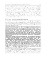
Fig. 3. a) Electroluminescence spectra of compounds 1-6 spanning from green to near IR; b)
Current-voltage (I -V), luminance–voltage (L -V) characteristics (left) and EL efficiency
(right) of the device obtained with compounds 3 as the active layer (120-nm-thick with a 70-
nm-thick PEDOT layer).
The maximum luminance reached using compound 3 (Figure 3b) was 400 cd/m
2
at 20 V, a
value which was already good enough for display applications. The device with compound
3 displayed also the highest EL efficiency, 0.2%, which was at least one order of magnitude
larger rather than those already reported for the best oligo- and polythiophene based
devices. The devices obtained with compounds 1-6 showed that it was possible to obtain
multicolor electroluminescence from oligomeric thiophene materials and greatly improve
the electroluminesce characteristics compared to conventional oligomers.
3. V-shaped oligothiophene-S,S-dioxides with high photo and
electroluminescence performance
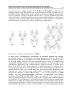
A remarkable improvement was achieved in 2003 with a new approach based on the
replacement of the conventional linear structure of oligothiophenes and oligothiophene-S,S-
dioxides with branched benzo[b]thiophene based structures (Mazzeo et al., 2003 a;
Barbarella et al. 2005).
These compounds (V-shaped oligothiophenes), in combination with
the oxygen functionalization of the core thienyl sulphur and the cyclohexyl substitution of
the lateral thienyl rings, allowed to achieve a remarkable luminance value of 10500 cd/m
2
,
which was the highest value obtained for LEDs based on oligothiophenes. The rationale
a
b
behind the synthesis of V-shaped compounds was the need to replace crystalline by
amorphous thin films in order to avoid strong intermolecular interactions and then reduce
the contribution of non radiative intermolecular deactivation pathways.
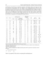
The molecular structure of selected V-shaped oligothiophenes is shown in Scheme 5, while
the corresponding electro-optical characteristics are reported in Table 2. The luminance vs.
voltage plots and the electroluminescence spectra of the devices fabricated with 9, 10 and 11
as the active materials, are shown in Figure 4.
Scheme 5. Molecular structure of V-shaped oligothiophene-S,S-dioxides 7-11. Cx =
Cyclohexyl.
%
Epc
Epa
Lum
M
(cd/m
2
)
%
7
4
<-2 1.60 35 0.001
8
2
<-2 1.35 1250 0.02
9
4
-1.26 1.43 2500 0.14
10
50
-1.45 >2 500 0.06
11
21
-1.36 1.48 10500 0.45
Table 2. Electro-optical characteristics of componds 7-11
a
a) : PL efficiency; Epc, Epa: reduction and oxidation peak potentials (vs calomel electrode)
measured by cyclovoltammetry; LumM : luminance max; : EL efficiency.
Table 2 shows that the functionalization of the benzothienyl moiety with oxygen affects
slightly the oxidation potentials but causes a relevant displacement of the reduction
potentials towards less negative values (by an amount up to 0.74 eV), indicating a marked
increase in the electron affinity of the compounds, in line with what was observed for linear
oligothiophene-S,S-dioxides. All compounds were employed as active layers in OLEDs in
which ITO/PEDOT:PSS and calcium/aluminum were used as the anode and the cathode,
respectively, i.e. the same conditions employed with linear oligothiophene-S,S-dioxides.
Most devices showed much better performance and operational stability than those
achieved using the linear oligomers.
Organic Light Emitting Diode12
Fig. 4. a) Luminance vs. voltage and b) electroluminescence spectra of devices fabricated
using compounds 9, 10 and 11.
Comparison of the the luminance values reported in tables 1 and 2, shows that the V-shaped
structure was crucial to improve the brightness of the devices. For example, the non
oxidized branched compound 8, shows a maximum brightness value of 1250 cd/m
2
, three
times higher than the best functionalized linear oligothiophene-S,S-dioxide reported in
Table 1. While, in contrast to linear oligothiophene-S,S-dioxides, the functionalization with
oxygen does not result in a substantial enhancement in photoluminescence efficiency, the EL
efficiency is significantly improved. This is shown, for example, by comparison of the
efficiency and luminance of the devices fabricated with compound 8 (0.02% and 1250 cd/m
2
,
respectively) and with the corresponding oxigenated derivative 9 (0.14% and 2400 cd/m
2
).
This result is due to the fact that the oxygen atoms induce a strong reduction in the energetic
barrier between the cathode and the emissive layer, as in linear oligothiophene-S,S-dioxides.
The maximum luminance (10500 cd/m
2
) for the LED fabricated with compound 11 is more
than 20 times larger than the maximum luminance displayed by the LED fabricated with the
corresponding linear oligothiophene-S,S-dioxide, i.e. compound 3 (400 cd/m
2
). As shown by
comparison of the data reported in tables 1-2, also the maximum luminance of the devices
based on compounds 9 (2500 cd/m
2
) and 10 (500 cd/m
2
) are much higher than those
obtained with the devices based on the corresponding linear compounds 5 (105 cd/m
2
) and
1 (100 cd/m
2
). Since theoretical calculations, optical and CV data indicate that V-shaped
oligothiophene-S,S-dioxides have electronic and optical features very similar to those of the
corresponding linear compounds, the reason for the improved performances was ascribed
to the much better film-forming properties of V-shaped compared to linear compounds and
to changes in morphology from crystalline to amorphous films. There are several studies in
the literature indicating that amorphous thin films, obtained either by vapor deposition or
spin coating, enhance the electroluminesce properties (Robinson et al., 2001; Su et al., 2002;
Doi et al., 2003).
The good film-forming properties and the amorphous morphology of V-shaped oligomers
are due to their branched structure and asymmetric molecular conformation. TD-DFT
calculations showed indeed that the molecular geometry of V-shaped oligothiophenes was
not planar due to the large dihedral angle (>60°) between the branch in the β-position and
the rigid core (Mazzeo et al., 2003).
The best performance of OLEDs based on V-shaped oligomers was obtained with the
oxigenated compound functionalized with β-cyclohexyl substituents, namely compound 11,
a
b
in which electronic de-excitation via intermolecular interactions and internal conversion
processes - which are the most important non radiative relaxation channels in
oligothiophene-S,S-dioxides (Lanzani et al., 2001; Della Sala et al., 2003; Anni et al., 2005) -
are strongly reduced. Functionalization with the bulky cyclohexyl groups has several effects.
First, the large intermolecular distances due to the bulky substituents reduce the
intermolecular interactions. Second, as shown by DFT (ground state) and TD-DFT (excited
state) molecular geometry optimizations (Mazzeo et al., 2003 a), the molecular distortion is
increased both in the ground and in the excited state. In the first singlet excited state the
thiophene branches lie in two different planes, making the formation of non radiative
aggregates unlikely. Third, the flexibility of the branches is strongly reduced. The
calculations show, for example, that while compounds 8 and 9 are very flexible and can exist
in different conformations of similar energy, for compound 11 only one ground-state energy
minimum is found. Thus, the cyclohexyl substituents stabilize the conformation and make
the molecule more rigid. All factors lead to enhanced photoluminescence in the solid state.
The luminance of 10500 cd/m
2
reached with the device based on compound 11 is one of the
highest values reported so far in the literature for devices with spin coated active layers.
Recently, OLEDs using as emitting layers nicely engineered branched oligomers
(compounds 12-13) containing a dibenzothiophene-S,S-dioxide core and triarylamine
branches, have been reported (Huang et al., 2006).
The thiophene-S,S-dioxide group was
introduced for its beneficial effect on the electron affinity of the molecules, while the triaryl
amino groups were introduced because of their beneficial effect on charge (holes) transport
and film forming properties. The molecular structure of compounds 12 and 13 is reported in
Scheme 6.
Scheme 6. Molecular structure of branched oligomers 12 and 13.
Organic light emitting diodes based
on functionalized oligothiophenes for display and lighting applications 13
Fig. 4. a) Luminance vs. voltage and b) electroluminescence spectra of devices fabricated
using compounds 9, 10 and 11.
Comparison of the the luminance values reported in tables 1 and 2, shows that the V-shaped
structure was crucial to improve the brightness of the devices. For example, the non
oxidized branched compound 8, shows a maximum brightness value of 1250 cd/m
2
, three
times higher than the best functionalized linear oligothiophene-S,S-dioxide reported in
Table 1. While, in contrast to linear oligothiophene-S,S-dioxides, the functionalization with
oxygen does not result in a substantial enhancement in photoluminescence efficiency, the EL
efficiency is significantly improved. This is shown, for example, by comparison of the
efficiency and luminance of the devices fabricated with compound 8 (0.02% and 1250 cd/m
2
,
respectively) and with the corresponding oxigenated derivative 9 (0.14% and 2400 cd/m
2
).
This result is due to the fact that the oxygen atoms induce a strong reduction in the energetic
barrier between the cathode and the emissive layer, as in linear oligothiophene-S,S-dioxides.
The maximum luminance (10500 cd/m
2
) for the LED fabricated with compound 11 is more
than 20 times larger than the maximum luminance displayed by the LED fabricated with the
corresponding linear oligothiophene-S,S-dioxide, i.e. compound 3 (400 cd/m
2
). As shown by
comparison of the data reported in tables 1-2, also the maximum luminance of the devices
based on compounds 9 (2500 cd/m
2
) and 10 (500 cd/m
2
) are much higher than those
obtained with the devices based on the corresponding linear compounds 5 (105 cd/m
2
) and
1 (100 cd/m
2
). Since theoretical calculations, optical and CV data indicate that V-shaped
oligothiophene-S,S-dioxides have electronic and optical features very similar to those of the
corresponding linear compounds, the reason for the improved performances was ascribed
to the much better film-forming properties of V-shaped compared to linear compounds and
to changes in morphology from crystalline to amorphous films. There are several studies in
the literature indicating that amorphous thin films, obtained either by vapor deposition or
spin coating, enhance the electroluminesce properties (Robinson et al., 2001; Su et al., 2002;
Doi et al., 2003).
The good film-forming properties and the amorphous morphology of V-shaped oligomers
are due to their branched structure and asymmetric molecular conformation. TD-DFT
calculations showed indeed that the molecular geometry of V-shaped oligothiophenes was
not planar due to the large dihedral angle (>60°) between the branch in the β-position and
the rigid core (Mazzeo et al., 2003).
The best performance of OLEDs based on V-shaped oligomers was obtained with the
oxigenated compound functionalized with β-cyclohexyl substituents, namely compound 11,
a
b
in which electronic de-excitation via intermolecular interactions and internal conversion
processes - which are the most important non radiative relaxation channels in
oligothiophene-S,S-dioxides (Lanzani et al., 2001; Della Sala et al., 2003; Anni et al., 2005) -
are strongly reduced. Functionalization with the bulky cyclohexyl groups has several effects.
First, the large intermolecular distances due to the bulky substituents reduce the
intermolecular interactions. Second, as shown by DFT (ground state) and TD-DFT (excited
state) molecular geometry optimizations (Mazzeo et al., 2003 a), the molecular distortion is
increased both in the ground and in the excited state. In the first singlet excited state the
thiophene branches lie in two different planes, making the formation of non radiative
aggregates unlikely. Third, the flexibility of the branches is strongly reduced. The
calculations show, for example, that while compounds 8 and 9 are very flexible and can exist
in different conformations of similar energy, for compound 11 only one ground-state energy
minimum is found. Thus, the cyclohexyl substituents stabilize the conformation and make
the molecule more rigid. All factors lead to enhanced photoluminescence in the solid state.
The luminance of 10500 cd/m
2
reached with the device based on compound 11 is one of the
highest values reported so far in the literature for devices with spin coated active layers.
Recently, OLEDs using as emitting layers nicely engineered branched oligomers
(compounds 12-13) containing a dibenzothiophene-S,S-dioxide core and triarylamine
branches, have been reported (Huang et al., 2006).
The thiophene-S,S-dioxide group was
introduced for its beneficial effect on the electron affinity of the molecules, while the triaryl
amino groups were introduced because of their beneficial effect on charge (holes) transport
and film forming properties. The molecular structure of compounds 12 and 13 is reported in
Scheme 6.
Scheme 6. Molecular structure of branched oligomers 12 and 13.
Organic Light Emitting Diode14
Fig. 5. Luminance versus current density characteristics for single layer devices of
compounds 12 and 13. Structure of the devices: I) ITO/12 (or 13) (40 nm)/TPBI (40 nm)/LiF
(1 nm)/Al (150 nm); II) ITO/NPB (40 nm)/12 (or 13) (40 nm)/LiF (1 nm)/Al (150 nm); III)
ITO/12 (or 13) (80 nm)/LiF (1 nm)/Al (150 nm).
Using compounds 12 and 13, excellent luminances were obtained with single layer (spin
coated) devices, as shown in Figure 5. The optical characteristics of compounds 12-13 and
the relevant parametrs of the devices based on these compounds are reported in Table 3.
12 13
V
on
[V] 2.5, 2.3, 2.2 2.2, 2.5, 2.0
L
max
[cdm
–2
]
85475 (12.5), 9537
(15.0)
40140 (13.0) 10521
(11.5)
(V at L
max
,[V]) 37699 (12.5) 25159 (14.5)
em
[nm] 492, 492, 496 540, 536, 542
ext,max
[%] 4.9, 1.3, 3.1 1.4, 0.87, 1.3
p,max
[lmW
–1
] 9.7, 3.3, 7.2 4.9, 3.3, 5.0
c,max
[cdA
–1
] 11, 3.1, 7.7 5.1, 3.1, 4.7
L [cd m
–2
]
[a]
10778, 2107, 7529 4904, 2272, 4245
ext
[%]
[a
4.7, 0.94, 3.1 1.4, 0.65, 1.2
p
[lmW
–1
]
[a]
6.5, 1.3, 3.9 2.8, 1.7, 2.1
c
[cdA
–1
]
[a]
10.8, 2.1, 7.5 4.9, 2.3, 4.2
Table 3. Optical characteristics of compounds 12-13 and performance of the corresponding
devices
a
a) Von: turn-on voltage; Lmax: maximum luminance;
ext,max: maximum external
quantum efficiency;
p,max: maximum power efficiency;
c,max: maximum current
efficiency.
[a] Measured at a current density of 100 mAcm
–2
. V
on
was obtained from the x-intercept of a
plot of log(luminance) vs applied voltage
A maximum luminance value of about 90000 cd/m
2
at 1300 mA/cm
2
was reached for 13 and
of about 90000 cd/m
2
at a similar current density for 2. The good performance of the devices
was likely to be related to a much better balance of electron- and hole-transport properties
than that achieved with linear or V-shaped oligothiophene-S,S-dioxides.
These results underline the potential impact that molecules containing thiophene-S,S-
dioxide moieties could have on light emitting devices if more sophisticated device structures
were realized with these materials.
4. Oligothiophenes for white OLEDs applications
Application in displays is only one among the several possible technological developments
of oligomeric thiophene materials. Another important application is in the lighting sector
where the replacement of standard white sources with flat organic devices is currently a
matter of intense research.
One of the first approaches to realize white OLEDs (WOLEDs) using thiophene materials
consisted in exploiting the high electron affinity of 2,5-bis-trimethylsilyl-thiophene-1,1-
dioxide (STO) used as acceptor to generate exciplex states in combination with a very low
electron affinity material (triphenyldiamine, TPD) used a donor (Mazzeo et al., 2003 b).
Figure 6 shows the molecular structure of both TPD and STO. While the electron affinity of
TPD is around 2,3 eV, that of STO is around 3,0 eV, i.e. close to that of longer linear
oligothiophene-S,S-dioxides. The reason for this is in the fact that the LUMO state of the
longer compounds is almost entirely localized in the central oxidized ring (Della Sala et al.,
2003; Anni et al., 2005).
Once the exciton is formed on the TPD molecule, the electron can
move to a near STO molecule, with higher electron affinity. In consequence, two radiative
transitions become allowed, one from the TPD molecules and the other from the transition
between the LUMO level of STO and the HOMO level of TPD. As a result, a peak at 420 nm
and a band at 570 nm are obtained, the two transitions resulting in white emission.
In Figure 6, PL spectra and images of blended films with different relative donor/acceptor
concentrations, spin-coated on quartz substrates, are reported. It is seen that enhancing the
concentration of STO a broad red-shifted emission due to exciplex states appears, in
addition to the blue emission due to TPD, which is responsible for the white emission within
a concentration range 17-53% of STO in TPD. The normalized EL spectra were similar to the
PL spectra for the concentration used (20%), showing that the shape of the low-energy
exciplex spectrum is almost independent of the applied voltage.
The CIE coordinates of the
EL spectra indicated a balanced white emission (0.39, 0.40) (Mazzeo et al., 2003 b).
Organic light emitting diodes based
on functionalized oligothiophenes for display and lighting applications 15
Fig. 5. Luminance versus current density characteristics for single layer devices of
compounds 12 and 13. Structure of the devices: I) ITO/12 (or 13) (40 nm)/TPBI (40 nm)/LiF
(1 nm)/Al (150 nm); II) ITO/NPB (40 nm)/12 (or 13) (40 nm)/LiF (1 nm)/Al (150 nm); III)
ITO/12 (or 13) (80 nm)/LiF (1 nm)/Al (150 nm).
Using compounds 12 and 13, excellent luminances were obtained with single layer (spin
coated) devices, as shown in Figure 5. The optical characteristics of compounds 12-13 and
the relevant parametrs of the devices based on these compounds are reported in Table 3.
12 13
V
on
[V] 2.5, 2.3, 2.2 2.2, 2.5, 2.0
L
max
[cdm
–2
]
85475 (12.5), 9537
(15.0)
40140 (13.0) 10521
(11.5)
(V at L
max
,[V]) 37699 (12.5) 25159 (14.5)
em
[nm] 492, 492, 496 540, 536, 542
ext,max
[%] 4.9, 1.3, 3.1 1.4, 0.87, 1.3
p,max
[lmW
–1
] 9.7, 3.3, 7.2 4.9, 3.3, 5.0
c,max
[cdA
–1
] 11, 3.1, 7.7 5.1, 3.1, 4.7
L [cd m
–2
]
[a]
10778, 2107, 7529 4904, 2272, 4245
ext
[%]
[a
4.7, 0.94, 3.1 1.4, 0.65, 1.2
p
[lmW
–1
]
[a]
6.5, 1.3, 3.9 2.8, 1.7, 2.1
c
[cdA
–1
]
[a]
10.8, 2.1, 7.5 4.9, 2.3, 4.2
Table 3. Optical characteristics of compounds 12-13 and performance of the corresponding
devices
a
a) Von: turn-on voltage; Lmax: maximum luminance;
ext,max: maximum external
quantum efficiency;
p,max: maximum power efficiency;
c,max: maximum current
efficiency.
[a] Measured at a current density of 100 mAcm
–2
. V
on
was obtained from the x-intercept of a
plot of log(luminance) vs applied voltage
A maximum luminance value of about 90000 cd/m
2
at 1300 mA/cm
2
was reached for 13 and
of about 90000 cd/m
2
at a similar current density for 2. The good performance of the devices
was likely to be related to a much better balance of electron- and hole-transport properties
than that achieved with linear or V-shaped oligothiophene-S,S-dioxides.
These results underline the potential impact that molecules containing thiophene-S,S-
dioxide moieties could have on light emitting devices if more sophisticated device structures
were realized with these materials.
4. Oligothiophenes for white OLEDs applications
Application in displays is only one among the several possible technological developments
of oligomeric thiophene materials. Another important application is in the lighting sector
where the replacement of standard white sources with flat organic devices is currently a
matter of intense research.
One of the first approaches to realize white OLEDs (WOLEDs) using thiophene materials
consisted in exploiting the high electron affinity of 2,5-bis-trimethylsilyl-thiophene-1,1-
dioxide (STO) used as acceptor to generate exciplex states in combination with a very low
electron affinity material (triphenyldiamine, TPD) used a donor (Mazzeo et al., 2003 b).
Figure 6 shows the molecular structure of both TPD and STO. While the electron affinity of
TPD is around 2,3 eV, that of STO is around 3,0 eV, i.e. close to that of longer linear
oligothiophene-S,S-dioxides. The reason for this is in the fact that the LUMO state of the
longer compounds is almost entirely localized in the central oxidized ring (Della Sala et al.,
2003; Anni et al., 2005).
Once the exciton is formed on the TPD molecule, the electron can
move to a near STO molecule, with higher electron affinity. In consequence, two radiative
transitions become allowed, one from the TPD molecules and the other from the transition
between the LUMO level of STO and the HOMO level of TPD. As a result, a peak at 420 nm
and a band at 570 nm are obtained, the two transitions resulting in white emission.
In Figure 6, PL spectra and images of blended films with different relative donor/acceptor
concentrations, spin-coated on quartz substrates, are reported. It is seen that enhancing the
concentration of STO a broad red-shifted emission due to exciplex states appears, in
addition to the blue emission due to TPD, which is responsible for the white emission within
a concentration range 17-53% of STO in TPD. The normalized EL spectra were similar to the
PL spectra for the concentration used (20%), showing that the shape of the low-energy
exciplex spectrum is almost independent of the applied voltage.
The CIE coordinates of the
EL spectra indicated a balanced white emission (0.39, 0.40) (Mazzeo et al., 2003 b).
Organic Light Emitting Diode16
Fig. 6. Molecular structure of TPD and STO (left); PL spectra of the blends realized through
TPD and STO (middle) and images of the blends in solid state films (right).
Although these results were promising for the generation of a new class of devices, their
luminance was not very high. Much better results were obtained with a different approach,
i.e. using a single thiophene material emitting in the white by virtue of its supramolecular
organization (Mazzeo et al., 2005). The material in question is 3,5-dimethyl-2,6-
bis(dimesitylboryl)-dithieno[3,2-b:2’,3’-d]thiophene, whose molecular structure is reported
in Figure 7.
Fig. 7. Molecular structure of 3,5-dimethyl-2,6-bis(dimesitylboryl)-dithieno[3,2-
b:2’,3’d]thiophene and PL spectrum in solution (left) and in the solid state (right).
% S TO
0
9
17
33
53
67
83
100
% S TO
0
9
17
33
53
67
83
100
400 500 600 700 800
% STO
83
67
33
53
17
9
100
0
Intensity (arb. units)
W avelength (nm )
S
S
S
B
B
Figure 7 shows that while in solution only a blue-green emission is observed, in the solid
state an additional narrow red-shifted emission at 680 nm is also present in the PL spectrum.
This red shifted absorption was peculiar to the solid state and could not be observed in
solution in the concentration range 10
-5
– 10
-2
M. The appearance of similar red shifted
absorption peaks had already been reported for several organic compounds and were
assigned to triplets activated in the solid state or particular aggregation states (Lupton et al.,
2003).
By the aid of time-resolved photoluminescence (TR-PL) the red-shifted emission could
be ascribed to the formation of aggregates or excimers. However, contrary to what it is
generally observed with aggregates and excimers that are characterised by broad PL spectra
(Lupton et al., 2003),
the linewidth of the peak at 680 nm was narrow. In order to elucidate
this point, INDO/SCI calculations were carried out. The calculations suggested that the
narrow line was the result of the very peculiar supramolecular arrangement assumed by the
compound in the aggregated state (Mazzeo et al., 2005).
Indeed, due to the planar and rigid
conformation of the inner dithienothiophene core and the presence of the bulky mesityl
substituents, the molecules tend to fit together in a cross-like configuration as shown in
Figure 8. Only very small movements of the molecules through translations along the x-y
axis, or small angular () deviations are allowed.
Fig. 8. Molecular structure of two interacting molecules forming a cross-like dimer (left) and
(right) Intermediate neglect of differential overlap/single configuration interaction
(INDO/SCI) excitation-energy shifts due to intermolecular interactions. The scale on the
right corresponds to calculated excitation energy shifts.
Commonly observed HB-type dimeric aggregates (i.e. with =180) are completely
forbidden for this rigid compound, due to the repulsion of the mesityl substituents. In such
fixed cross-like configuration the peak broadening induced by supramolecular
conformational dispersion is strongly reduced. The plot reported in Figure 8 shows that the
excitation energy shift is indeed dominated by only one deep minimum. This means that
only one single arrangement is responsible for the additional red emission observed in the
solid state, leading to a very narrow emission. The calculations also showed that this kind of
intermolecular arrangement induces a red-shift as high as 0.55 eV, a value which is in good
agreement with the experimental result (0.7 eV).
The white emitting dithienothiophene derivative displayed good film forming properties
and could be used as active material in light emitting diodes. The emissive layer was spin-
coated between ITO/PEDOT:PSS and LiF/Al, used as anode and cathode, respectively. The
Organic light emitting diodes based
on functionalized oligothiophenes for display and lighting applications 17
Fig. 6. Molecular structure of TPD and STO (left); PL spectra of the blends realized through
TPD and STO (middle) and images of the blends in solid state films (right).
Although these results were promising for the generation of a new class of devices, their
luminance was not very high. Much better results were obtained with a different approach,
i.e. using a single thiophene material emitting in the white by virtue of its supramolecular
organization (Mazzeo et al., 2005). The material in question is 3,5-dimethyl-2,6-
bis(dimesitylboryl)-dithieno[3,2-b:2’,3’-d]thiophene, whose molecular structure is reported
in Figure 7.
Fig. 7. Molecular structure of 3,5-dimethyl-2,6-bis(dimesitylboryl)-dithieno[3,2-
b:2’,3’d]thiophene and PL spectrum in solution (left) and in the solid state (right).
% S TO
0
9
17
33
53
67
83
100
% S TO
0
9
17
33
53
67
83
100
400 500 600 700 800
% STO
83
67
33
53
17
9
100
0
Intensity (arb. units)
W avelength (nm )
S
S
S
B
B
Figure 7 shows that while in solution only a blue-green emission is observed, in the solid
state an additional narrow red-shifted emission at 680 nm is also present in the PL spectrum.
This red shifted absorption was peculiar to the solid state and could not be observed in
solution in the concentration range 10
-5
– 10
-2
M. The appearance of similar red shifted
absorption peaks had already been reported for several organic compounds and were
assigned to triplets activated in the solid state or particular aggregation states (Lupton et al.,
2003).
By the aid of time-resolved photoluminescence (TR-PL) the red-shifted emission could
be ascribed to the formation of aggregates or excimers. However, contrary to what it is
generally observed with aggregates and excimers that are characterised by broad PL spectra
(Lupton et al., 2003),
the linewidth of the peak at 680 nm was narrow. In order to elucidate
this point, INDO/SCI calculations were carried out. The calculations suggested that the
narrow line was the result of the very peculiar supramolecular arrangement assumed by the
compound in the aggregated state (Mazzeo et al., 2005).
Indeed, due to the planar and rigid
conformation of the inner dithienothiophene core and the presence of the bulky mesityl
substituents, the molecules tend to fit together in a cross-like configuration as shown in
Figure 8. Only very small movements of the molecules through translations along the x-y
axis, or small angular () deviations are allowed.
Fig. 8. Molecular structure of two interacting molecules forming a cross-like dimer (left) and
(right) Intermediate neglect of differential overlap/single configuration interaction
(INDO/SCI) excitation-energy shifts due to intermolecular interactions. The scale on the
right corresponds to calculated excitation energy shifts.
Commonly observed HB-type dimeric aggregates (i.e. with =180) are completely
forbidden for this rigid compound, due to the repulsion of the mesityl substituents. In such
fixed cross-like configuration the peak broadening induced by supramolecular
conformational dispersion is strongly reduced. The plot reported in Figure 8 shows that the
excitation energy shift is indeed dominated by only one deep minimum. This means that
only one single arrangement is responsible for the additional red emission observed in the
solid state, leading to a very narrow emission. The calculations also showed that this kind of
intermolecular arrangement induces a red-shift as high as 0.55 eV, a value which is in good
agreement with the experimental result (0.7 eV).
The white emitting dithienothiophene derivative displayed good film forming properties
and could be used as active material in light emitting diodes. The emissive layer was spin-
coated between ITO/PEDOT:PSS and LiF/Al, used as anode and cathode, respectively. The
Organic Light Emitting Diode18
LiF layer was employed in order to enhance the carrier injection in the emissive layer (Hung
et al., 1997).
The EL spectrum at a LiF thickness of ≈ 5 nm and the device performance are
shown in Figure 9.
Fig. 9. EL spectrum of device with d
LiF ≈
5nm (left) (inset: image of a large area device);
Luminance-current density-voltage characteristics (right).
For 4.8 nm of LiF the performances are 50 times higher than the device in which only the
Aluminium was used as cathode. In particular, a brightness of 3800 cd/m
2
at 18 V (Figure 9)
and a maximum QE of 0.35% could be achieved. It is worth noting that the luminance of this
device overcomes the minimum value of 1000 cd/m
2
required for lighting systems. The
white electroluminescence was achieved by the superposition of the broad blue-green
emission originating from the single molecule and the red-shifted narrow peak assigned to
the formation of cross-like dimers in the solid-state. This was one of the first examples in the
literature of white emission from a single molecular material in the solid state. The good
performance of the device was due to an unusual mixing of favourable factors, i.e. the very
peculiar self-organization properties of the dithienothiophene derivative, the well known
electron-acceptor properties of the boron atom and the good film forming properties of the
material. Nevertheless, the results obtained, indicate that the fabrication of a new class of
white emitting devices combining the simplicity and low-cost of single layer spin-coated
devices is achievable through appropriate molecular engineering.
5. Very low voltage and stable oligothiophene OLEDs.
As shown in the previous section, thiophene oligomeric materials have great potential for
application in displays and lighting. All the devices described in the previous sections have
been realized in a single-layer or bilayer configuration by depositing the active material by
spin coating. This is a strong limitation for oligomeric materials since, even if the material is
highly performant in terms of PL, the devices are not efficient enough due to the limits of
wet deposition processes like spin coating. Polymeric materials have the same type of
problems. However, while polymeric materials cannot be evaporated, this is possible for
oligomeric materials owing to their small molecular weight. Thus, a possible improvement
in OLEDs based on thiophene oligomeric materials can be realized if these compounds are
deposited in a heterostructure system (Walzer et al., 2007; Zhou et al., 2001; Huang et al.,
400 500 600 700 800
EL Intensity (a.u.)
Wavelenght (nm)
2002).
So far, no attempts have been made in this direction and the data shown below are the
first reported to date.
We fabricated a much more sophisticated device using compound 3 (Mariano et al., 2009)
and, to check the limit in brightness and stability of the compound, we realized an OLED
based on electrically doped transport layers, i.e. in the so-called p-i-n (p-type-intrinsic-n-
type) configuration (Walzer et al., 2007).
In order to obtain low driving voltages, low ohmic losses at the interface between the metal
and the transport layers are an important factor. Organic light-emitting diodes are usually
realized with un-doped thin organic films, requiring high operating voltages to overcome
the energy barriers between the contacts and the transport layers and to drive the opposite
charges into the emissive layer. Contrary to inorganic LEDs, the typical driving voltage is
much higher than the thermodynamic limit, which is given by the energy gap of the active
layer. Recently, controlled electrical doping in transport layers of the OLEDs has been
introduced (Walzer et al., 2007; Zhou et al., 2001; Huang et al., 2002).
The typical dopants
explored have been the 2,3,5,6-tetrafluoro-7,7,8,8 tetracyanoquinodimethane (F4TCNQ) as
donor of holes in an hole transport layer and alkali metals such as Cs or Li as donors of
electrons in an electron transport layer. The doping of the transport layers leads to the
formation of thin space charge layers which are formed at the interface with the metal
contact layer, allowing for a good injection (ohmic) of the carriers by tunneling despite the
barriers. This effect removes completely the energy barrier between the metal layers ad the
transport layers, thus reducing the voltage. Moreover, the high electrical conductivity of the
doped layers reduces also the drop in voltage caused by the usually high resistance of the
undoped organic films. The p and n-doping of the transporting layers permits to reach a
conductivity of 10
-5
S/cm, which is enough in order to have a negligible drop in the voltage
across these layers. Due to the incorporation of these very conductive transporting layers,
which form Ohmic contacts with the electrodes, p-i-n architectures supply more current
density than conventional OLEDs, under the same driving voltage (Zhou et al., 2001; Huang
et al., 2002). Therefore, higher brightness can be obtained at low bias.
This type of OLED has an electrically intrinsic emission layer (EML), a hole transport layer
(HTL) and an electron transport layer (ETL). Additional blocking layers between the charge
transport layers and the emissive layer are generally also introduced to prevent problems
related to the lack of charge balance, exciton quenching by excess of charge carriers, and
exciplexes formation at the interface. All these layers complicate the structure of the device
but increase its efficiency and stability. The aim of p-i-n technology is to reduce the applied
voltage in order to have a given luminance and improve power efficiency giving more
stability to the device and less power consumption.
The structure of the device realized with the linear oligothiophene-S,S-dioxide 3 (whose
molecular structure is shown in Scheme 4) is shown in Figure 10. It consists of the following
layers: ITO transparent anode; a 35 nm thick layer of N,N,N’,N’ tetrakis(4-methoxyphenyl)-
benzidine (MeO-TPD) doped with 2.7 wt % of 2,3,5,6-tetrafluoro-7,7,8,8
tetracyanoquinodimethane (F4-TCNQ) that was evaporated as p-doped hole injection and
transport layer; a 7 nm thick film of 2,2’,7,7’-tetrakis-(diphenylamino)-9,9’-spirobifluorene
(Spiro-TAD) which acts as electron blocking layer; an emitting layer consisting of 30 nm of
compound 3 of Figure 5; 10 nm of 4, 7-diphenyl-1,10-phenanthroline (Bphen) as hole
blocking layer; 35 nm of Bphen doped with Cs as electrons injecting and transporting layer;
Organic light emitting diodes based
on functionalized oligothiophenes for display and lighting applications 19
LiF layer was employed in order to enhance the carrier injection in the emissive layer (Hung
et al., 1997).
The EL spectrum at a LiF thickness of ≈ 5 nm and the device performance are
shown in Figure 9.
Fig. 9. EL spectrum of device with d
LiF ≈
5nm (left) (inset: image of a large area device);
Luminance-current density-voltage characteristics (right).
For 4.8 nm of LiF the performances are 50 times higher than the device in which only the
Aluminium was used as cathode. In particular, a brightness of 3800 cd/m
2
at 18 V (Figure 9)
and a maximum QE of 0.35% could be achieved. It is worth noting that the luminance of this
device overcomes the minimum value of 1000 cd/m
2
required for lighting systems. The
white electroluminescence was achieved by the superposition of the broad blue-green
emission originating from the single molecule and the red-shifted narrow peak assigned to
the formation of cross-like dimers in the solid-state. This was one of the first examples in the
literature of white emission from a single molecular material in the solid state. The good
performance of the device was due to an unusual mixing of favourable factors, i.e. the very
peculiar self-organization properties of the dithienothiophene derivative, the well known
electron-acceptor properties of the boron atom and the good film forming properties of the
material. Nevertheless, the results obtained, indicate that the fabrication of a new class of
white emitting devices combining the simplicity and low-cost of single layer spin-coated
devices is achievable through appropriate molecular engineering.
5. Very low voltage and stable oligothiophene OLEDs.
As shown in the previous section, thiophene oligomeric materials have great potential for
application in displays and lighting. All the devices described in the previous sections have
been realized in a single-layer or bilayer configuration by depositing the active material by
spin coating. This is a strong limitation for oligomeric materials since, even if the material is
highly performant in terms of PL, the devices are not efficient enough due to the limits of
wet deposition processes like spin coating. Polymeric materials have the same type of
problems. However, while polymeric materials cannot be evaporated, this is possible for
oligomeric materials owing to their small molecular weight. Thus, a possible improvement
in OLEDs based on thiophene oligomeric materials can be realized if these compounds are
deposited in a heterostructure system (Walzer et al., 2007; Zhou et al., 2001; Huang et al.,
400 500 600 700 800
EL Intensity (a.u.)
Wavelenght (nm)
2002).
So far, no attempts have been made in this direction and the data shown below are the
first reported to date.
We fabricated a much more sophisticated device using compound 3 (Mariano et al., 2009)
and, to check the limit in brightness and stability of the compound, we realized an OLED
based on electrically doped transport layers, i.e. in the so-called p-i-n (p-type-intrinsic-n-
type) configuration (Walzer et al., 2007).
In order to obtain low driving voltages, low ohmic losses at the interface between the metal
and the transport layers are an important factor. Organic light-emitting diodes are usually
realized with un-doped thin organic films, requiring high operating voltages to overcome
the energy barriers between the contacts and the transport layers and to drive the opposite
charges into the emissive layer. Contrary to inorganic LEDs, the typical driving voltage is
much higher than the thermodynamic limit, which is given by the energy gap of the active
layer. Recently, controlled electrical doping in transport layers of the OLEDs has been
introduced (Walzer et al., 2007; Zhou et al., 2001; Huang et al., 2002).
The typical dopants
explored have been the 2,3,5,6-tetrafluoro-7,7,8,8 tetracyanoquinodimethane (F4TCNQ) as
donor of holes in an hole transport layer and alkali metals such as Cs or Li as donors of
electrons in an electron transport layer. The doping of the transport layers leads to the
formation of thin space charge layers which are formed at the interface with the metal
contact layer, allowing for a good injection (ohmic) of the carriers by tunneling despite the
barriers. This effect removes completely the energy barrier between the metal layers ad the
transport layers, thus reducing the voltage. Moreover, the high electrical conductivity of the
doped layers reduces also the drop in voltage caused by the usually high resistance of the
undoped organic films. The p and n-doping of the transporting layers permits to reach a
conductivity of 10
-5
S/cm, which is enough in order to have a negligible drop in the voltage
across these layers. Due to the incorporation of these very conductive transporting layers,
which form Ohmic contacts with the electrodes, p-i-n architectures supply more current
density than conventional OLEDs, under the same driving voltage (Zhou et al., 2001; Huang
et al., 2002). Therefore, higher brightness can be obtained at low bias.
This type of OLED has an electrically intrinsic emission layer (EML), a hole transport layer
(HTL) and an electron transport layer (ETL). Additional blocking layers between the charge
transport layers and the emissive layer are generally also introduced to prevent problems
related to the lack of charge balance, exciton quenching by excess of charge carriers, and
exciplexes formation at the interface. All these layers complicate the structure of the device
but increase its efficiency and stability. The aim of p-i-n technology is to reduce the applied
voltage in order to have a given luminance and improve power efficiency giving more
stability to the device and less power consumption.
The structure of the device realized with the linear oligothiophene-S,S-dioxide 3 (whose
molecular structure is shown in Scheme 4) is shown in Figure 10. It consists of the following
layers: ITO transparent anode; a 35 nm thick layer of N,N,N’,N’ tetrakis(4-methoxyphenyl)-
benzidine (MeO-TPD) doped with 2.7 wt % of 2,3,5,6-tetrafluoro-7,7,8,8
tetracyanoquinodimethane (F4-TCNQ) that was evaporated as p-doped hole injection and
transport layer; a 7 nm thick film of 2,2’,7,7’-tetrakis-(diphenylamino)-9,9’-spirobifluorene
(Spiro-TAD) which acts as electron blocking layer; an emitting layer consisting of 30 nm of
compound 3 of Figure 5; 10 nm of 4, 7-diphenyl-1,10-phenanthroline (Bphen) as hole
blocking layer; 35 nm of Bphen doped with Cs as electrons injecting and transporting layer;
Organic Light Emitting Diode20
200 nm Al deposited as cathode. The optically thick metallic film acts as a reflector and
thereby aids the output coupling of light from the device.
All films were deposited by thermal evaporation in a base pressure of about 10
-8
mbar, at a
rate in the range 0.5-1.0 Å/s. Before the deposition of the organic compounds, ITO
substrates were cleaned in acetone, isopropanol and deionized water for 10 min at 60 °C in
an ultrasonic bath. No plasma oxygen was performed because of the electrical doping of the
transport layers.
Figure 10a shows the luminance and the current density of the device as a function of the
voltage. The turn-on voltage was around 2.1 V, while the luminance reached the remarkable
value of 11000 cd/m
2
at only 9 V. The device showed a maximum EQE of 0.55%. It is worth
noting that the same material deposited by spincoating in a bilayer configuration shows a
maximum luminance of about 400 cd/m
2
obtained at the very high voltage of 19 V (Table 1).
This result obtained with the LED in p-i-n configuration underlines how all the properties of
the device can be strongly improved thanks to the possibility of vacuum evaporating
oligomeric materials.
The device reported in Figure 10 was encapsulated using a lid attached to the sample by an
epoxy resin in order to carry out aging measurements and to check the stability of both the
device and the material. We recall that the lifetime of OLEDs is defined as the time taken to
reach half of the starting luminance.
Fig. 10. Top: device structure. Bottom: (A) Luminance-Current Density vs. Voltage (left);
Luminance decay time for a starting value of 5500Cd/m
2
at fixed current density (right).
Figure 10b shows the plot of the luminance as a function of time for a starting value of 5500
cd/m
2
at a fixed current density of 320 mA/cm
2
. The black curve represents the
experimental data while the dotted curve represents the extrapolated behavior. The figure
0,1 1 10 100 1000
2500
3000
3500
4000
4500
5000
5500
6000
Luminance (cd/m
2
)
Time (h)
Lifetime curve starting from 5500cd/m
2
Extrapolation of the lifetime curve
-2 0 2 4 6 8 10
1E-4
1E-3
0,01
0,1
1
10
100
1000
Voltage (V)
Curr. Density (mA/cm
2
)
10
100
1000
10000
Luminance (Cd/m
2
)
Bphen: 4, 7-diphenyl-1,10-phenanthroline
STAD: 2,2’,7,7’-tetrakis-(diphenylamino)–
-9,9’-spirobifluorene
BAlq: bis-(2-methyl-8-quinolinolato)-4-
-(phenyl-phenolato) aluminum-III
MeO-TPD: N,N,N’,N’ tetrakis (4-methoxyphenyl)-
benzidine (MeO-TPD)
F4-TCNQ: 2,3,5,6-tetrafluoro-7,7,8,8 tetracyano-
-quinodimethane
shows that a remarkable lifetime of about 270 hours was reached. This result demonstrates
that heterostructure devices are the tools where thiophene oligomeric materials should be
tested to reveal all their potential as emissive compounds. Moreover, the demonstration that
oligthiophene-S,S-dioxides show very high stability is an important step forward that allows
to classify these materials among the best so far available for electroluminescence (Mariano
et al., 2009).
6. Conclusions and Outlook
Today, the field of electroluminescence of organic semiconductors is dominated by two
kinds of materials: phosphorescent and fluorescent small molecules, in particular for
applications where high emission power is needed, like lighting. Although phosphorescent
compounds seem to be the most promising in terms of external quantum efficiency and low
power consumption, fluorescent compounds show high stability and the possibility to be
deposited avoiding codeposition with a host. This is particularly true for oligothiophenes
which show high stability and the possibility to tune the emission wavelength in a very
wide range, from green-bluish to near infrared without the need of coevaporation. The
possibility to functionalize these compounds in a very flexible way and finely tailor their
properties, make this class of molecules strongly competitive with respect to standard ones
(also phosphorescent), although much research must still be carried out to further improve
the stability and the efficiency of devices based on these materials. We are currently pushing
up this research field trying to mix the best technology for OLEDs (p-i-n technology) with
the best thiophene oligomeric materials with the aim to generate new kinds of
electroluminescent devices for different pourposes: from display to lighting and automotive.
7. References
Amir, E. & Rozen, S. (2005). Angew. Chem. Int. Ed., 44, p. 7374.
Anni, M.; Della Sala, F.; Raganato, M. F.; Fabiano, E.; Lattante, S.; Cingolani, R.; Gigli, G.;
Barbarella, G.; Favaretto, L. & Görling, A. (2005). J. Phys. Chem. B, 109, p. 6004.
Antolini, L.; Tedesco, E.; Barbarella, G.; Favaretto, L.; Sotgiu, G.; Zambianchi, M.; Casarini,
M. D.; Gigli, G. Cingolani, R. (2000). J. Am. Chem. Soc., 122, p. 9006.
Baldo, M. A.; O’Brien, D. F.; You, Y.; Shoustikov, A.; Sibley, S.; Thompson, M. E. & Forrest,
S. R. (1998). Nature, 395, p. 151.
Baldo, M. A.; Thompson, M. E. & S. R. Forrest. (2000). Nature, 403, p. 750.
a) Barbarella, G.; Favaretto, L.; Zambianchi, M.; Pudova, O.; Arbizzani, C.; Bongini, A. &
Mastragostino, M. (1998). Adv.Mater., 10, p. 551.
b) Barbarella, G.; Favaretto, L.; Sotgiu, G.; Zambianchi, G.; Antolini, L.; Pudova,O. &
Bongini, A. (1998). J.Org.Chem., 63, p. 5497.
Barbarella, G.; Favaretto, L.; Sotgiu, G.; Zambianchi, M.; Fattori, V.; Cocchi, M.; Cacialli, F.;
Gigli, G. & Cingolani, R. (1999). Adv.Mater., 11, p. 1375.
Barbarella, G.; Favaretto, L.; Sotgiu, G.; Zambianchi, M.; Bongini, A.; Arbizzani, C.;
Mastragostino, M.; Anni, M.; Gigli, G. & Cingolani, R. (2000). J. Am. Chem. Soc.,
122, p. 11971.
Barbarella, G.; Favaretto, L.; Sotgiu, G.; Antolini, L.; Gigli, G.; Cingolani, R. & Bongini, A.
(2001). Chem.Mater., 13, p. 4112.
Organic light emitting diodes based
on functionalized oligothiophenes for display and lighting applications 21
200 nm Al deposited as cathode. The optically thick metallic film acts as a reflector and
thereby aids the output coupling of light from the device.
All films were deposited by thermal evaporation in a base pressure of about 10
-8
mbar, at a
rate in the range 0.5-1.0 Å/s. Before the deposition of the organic compounds, ITO
substrates were cleaned in acetone, isopropanol and deionized water for 10 min at 60 °C in
an ultrasonic bath. No plasma oxygen was performed because of the electrical doping of the
transport layers.
Figure 10a shows the luminance and the current density of the device as a function of the
voltage. The turn-on voltage was around 2.1 V, while the luminance reached the remarkable
value of 11000 cd/m
2
at only 9 V. The device showed a maximum EQE of 0.55%. It is worth
noting that the same material deposited by spincoating in a bilayer configuration shows a
maximum luminance of about 400 cd/m
2
obtained at the very high voltage of 19 V (Table 1).
This result obtained with the LED in p-i-n configuration underlines how all the properties of
the device can be strongly improved thanks to the possibility of vacuum evaporating
oligomeric materials.
The device reported in Figure 10 was encapsulated using a lid attached to the sample by an
epoxy resin in order to carry out aging measurements and to check the stability of both the
device and the material. We recall that the lifetime of OLEDs is defined as the time taken to
reach half of the starting luminance.
Fig. 10. Top: device structure. Bottom: (A) Luminance-Current Density vs. Voltage (left);
Luminance decay time for a starting value of 5500Cd/m
2
at fixed current density (right).
Figure 10b shows the plot of the luminance as a function of time for a starting value of 5500
cd/m
2
at a fixed current density of 320 mA/cm
2
. The black curve represents the
experimental data while the dotted curve represents the extrapolated behavior. The figure
0,1 1 10 100 1000
2500
3000
3500
4000
4500
5000
5500
6000
Luminance (cd/m
2
)
Time (h)
Lifetime curve starting from 5500cd/m
2
Extrapolation of the lifetime curve
-2 0 2 4 6 8 10
1E-4
1E-3
0,01
0,1
1
10
100
1000
Voltage (V)
Curr. Density (mA/cm
2
)
10
100
1000
10000
Luminance (Cd/m
2
)
Bphen: 4, 7-diphenyl-1,10-phenanthroline
STAD: 2,2’,7,7’-tetrakis-(diphenylamino)–
-9,9’-spirobifluorene
BAlq: bis-(2-methyl-8-quinolinolato)-4-
-(phenyl-phenolato) aluminum-III
MeO-TPD: N,N,N’,N’ tetrakis (4-methoxyphenyl)-
benzidine (MeO-TPD)
F4-TCNQ: 2,3,5,6-tetrafluoro-7,7,8,8 tetracyano-
-quinodimethane
shows that a remarkable lifetime of about 270 hours was reached. This result demonstrates
that heterostructure devices are the tools where thiophene oligomeric materials should be
tested to reveal all their potential as emissive compounds. Moreover, the demonstration that
oligthiophene-S,S-dioxides show very high stability is an important step forward that allows
to classify these materials among the best so far available for electroluminescence (Mariano
et al., 2009).
6. Conclusions and Outlook
Today, the field of electroluminescence of organic semiconductors is dominated by two
kinds of materials: phosphorescent and fluorescent small molecules, in particular for
applications where high emission power is needed, like lighting. Although phosphorescent
compounds seem to be the most promising in terms of external quantum efficiency and low
power consumption, fluorescent compounds show high stability and the possibility to be
deposited avoiding codeposition with a host. This is particularly true for oligothiophenes
which show high stability and the possibility to tune the emission wavelength in a very
wide range, from green-bluish to near infrared without the need of coevaporation. The
possibility to functionalize these compounds in a very flexible way and finely tailor their
properties, make this class of molecules strongly competitive with respect to standard ones
(also phosphorescent), although much research must still be carried out to further improve
the stability and the efficiency of devices based on these materials. We are currently pushing
up this research field trying to mix the best technology for OLEDs (p-i-n technology) with
the best thiophene oligomeric materials with the aim to generate new kinds of
electroluminescent devices for different pourposes: from display to lighting and automotive.
7. References
Amir, E. & Rozen, S. (2005). Angew. Chem. Int. Ed., 44, p. 7374.
Anni, M.; Della Sala, F.; Raganato, M. F.; Fabiano, E.; Lattante, S.; Cingolani, R.; Gigli, G.;
Barbarella, G.; Favaretto, L. & Görling, A. (2005). J. Phys. Chem. B, 109, p. 6004.
Antolini, L.; Tedesco, E.; Barbarella, G.; Favaretto, L.; Sotgiu, G.; Zambianchi, M.; Casarini,
M. D.; Gigli, G. Cingolani, R. (2000). J. Am. Chem. Soc., 122, p. 9006.
Baldo, M. A.; O’Brien, D. F.; You, Y.; Shoustikov, A.; Sibley, S.; Thompson, M. E. & Forrest,
S. R. (1998). Nature, 395, p. 151.
Baldo, M. A.; Thompson, M. E. & S. R. Forrest. (2000). Nature, 403, p. 750.
a) Barbarella, G.; Favaretto, L.; Zambianchi, M.; Pudova, O.; Arbizzani, C.; Bongini, A. &
Mastragostino, M. (1998). Adv.Mater., 10, p. 551.
b) Barbarella, G.; Favaretto, L.; Sotgiu, G.; Zambianchi, G.; Antolini, L.; Pudova,O. &
Bongini, A. (1998). J.Org.Chem., 63, p. 5497.
Barbarella, G.; Favaretto, L.; Sotgiu, G.; Zambianchi, M.; Fattori, V.; Cocchi, M.; Cacialli, F.;
Gigli, G. & Cingolani, R. (1999). Adv.Mater., 11, p. 1375.
Barbarella, G.; Favaretto, L.; Sotgiu, G.; Zambianchi, M.; Bongini, A.; Arbizzani, C.;
Mastragostino, M.; Anni, M.; Gigli, G. & Cingolani, R. (2000). J. Am. Chem. Soc.,
122, p. 11971.
Barbarella, G.; Favaretto, L.; Sotgiu, G.; Antolini, L.; Gigli, G.; Cingolani, R. & Bongini, A.
(2001). Chem.Mater., 13, p. 4112.
Organic Light Emitting Diode22
Barbarella, G.; Favaretto, L.; Zanelli, A.; Gigli, G.; Mazzeo, M.; Anni, M. & Bongini, A. (2005).
Adv. Funct. Mater., 15, p. 664.
Barta, P.; Cacialli, F.; Friend, R. H. & Zagórska, M. (1998). J. Appl. Phys., 84, p. 6279.
Beaupré, S. & Leclerc, M. (2002). Adv. Funct. Mater., 12, p. 192.
Berggren, M. Inganäs, O. Gustafsson, G. Rasmusson, J. Andersson, M. R. Hjertberg, T.
Wennersträm, O. (1994). Nature, 372, p. 444.
Berlin, A.; Zotti, G.; Zecchin, S.; Schiavon, G.; Cocchi, M.; Virgili, D. & Sabatini, C. (2003). J.
Mater. Chem., 13 , p. 27.
Braun, D.; Gustafsson, G.; McBranch, D. & Heeger, A. J. (1992). J. Appl. Phys., 72, p. 564- 568
Burroughes, J. H.; Bradley, D. D. C.; Brown, A. R.; Marks, R. N.; Friend, R. H.; Burn, P. L. &
Holmes, A. B. (1990). Nature, 347, p. 539.
Camaioni, N.; Ridolfi, G.; Fattori, V.; Favaretto, L. & Barbarella G. (2004). Appl. Phys. Lett.,
84, p. 1901.
Casado, J.; Zgierski, M. Z.; Ewbank, P. C.; Burand, M. W.; Janzen, D. E.; Mann, K. R.;
Pappenfus, T. M.; Berlin, A.; Pérez-Inestrosa, E.; Ortiz, R. P. & López Navarrete, J.
T. (2006). J. Am. Chem. Soc., 128, p. 10134.
Charas, A.; Morgado, J.; Martinho, J. M. G.; Alcácer, L. & Cacialli, F. (2001). Chem. Commun.,
p. 1216.
Cheylan, S.; Bolink, H.J.; Fraleoni-Morgera, A.; Puigdollers, J.; Voz, C.; Mencarelli, I.; Setti,
L.; Alcubilla, R. & Badenes, G. (2007). Organic Electronics, 8, p. 641.
Chou, P. T. & Chi, Y. (2007). Chem. Eur. J., 13, p. 380.
D’Andrade, B. W. & Forrest, S. R. (2004). Adv. Mater., 16, p. 1585.
D’Andrade, B. (2007). Nature Photonics , 1, p. 33.
Della Sala, F.; Raganato, M.F.; Anni, M.; Cingolani, R.; Weimer, M.; Görling, A.; Favaretto,
L.; Barbarella, G. & Gigli, G. (2003). Synth. Met., 139, p. 897.
Doi, H.; Kinoshita, M.; Okumoto, K. & Shirota, Y. (2003). Chem. Mater., 15, p. 1080.
F. Garnier (1999). Acc. Chem. Res., 32, p. 209.
Friend, R. H.; Gymer, R. W.; Holmes, A. B.; Burroughes, J. H.; Marks, R. N.; Taliani, C.;
Bradley, D. D. C.; Dos Santos, D. A.; Brédas, J. L.; Lögdlund, M. & Salaneck, W. R.
(1999). Nature, 397, p. 121.
Gigli, G.; Inganas, O.; Anni, M.; De Vittorio, M.; Cingolani, R.; Barbarella, G. & Favaretto, L.
(2001). Appl. Phys. Lett., 78, p. 1493.
Greenham, N. C.; Moratti, S. C.; Bradley, D. D. C.; Friend, R. H. & Holmes, A. B.
(1993). Nature, 365, p. 628.
Horowitz, G. Delannoy, P. Bouchriha, H. Deloffre, F. Fave, J L. Garnier, F. Hajlaoui, R.
Heyman, M. Kouki, F. Valat, P. Wittgens, V. & Yassar A. (1994). Adv. Mater., 6, p.
752.
Huang, J.; Pfeiffer, M.; Werner, A.; Blochwitz, J.; Leo, K. & Liu, S. (2002). Appl. Phys. Lett., 80,
p. 139.
Huang, T. H.; Lin, J. T.; Chen, L. Y.; Lin, Y. T. & Wu, C. C. (2006). Adv. Mater., 18, p. 602.
Hughes G. & Bryce, M. R. (2005). J. Mater. Chem., 15, p. 94.
Hung, L. S.; Tang, C. W. & Mason, M. G. (1997). Appl. Phys. Lett., 70, p. 152.
Hung, M. C.; Liao, J.L.; Chen, S. A.; Chen, S. H. & Su, A. C. (2005).
J. Am. Chem. Soc., 127, p.
14576.
Kalinowski, J. (2005). Organic Light-Emitting Diodes: Principles, Characteristics and Processes,
Marcel Dekker, New York.
Kanemitsu, Y. Shimizu, N. Suzuki, K. Shiraishi, Y. Kuroda, M. (1996). Phys. Rev. B , 54, p.
2198.
Kawamura, Y.; Goushi, K.; Brooks, J.; Brown, J. J.; Sasabe, H. & Adachi, C. (2005). Appl.
Phys. Lett., 86, p. 071104.
Kraft, A.; Grimsdale, A. C. & Holmes, A. B. (1998). Angew. Chem. Int. Ed., 37, p. 402.
Lanzani, G.; Cerullo, C.; De Silvestri, S.; Barbarella, G. & Sotgiu, G. (2001). J.Chem.Phys., 115,
p. 1623.
Liu, Y. L.; Feng, J. K. & Ren, A. M. (2008). J. Phys. Chem. A, 112, p. 3157.
Lupton, J. M.; Craig, M. R. & Meijer, E. W. (2002). Appl. Phys. Lett., 80, p. 4489.
Mariano, F.; Mazzeo, M.; Duan, Y.; Barbarella, G.; Favaretto, L.; Carallo, S.; Cingolani, R. &
Gigli, G. (2009). Appl. Phys. Lett., 94, p. 063510.
Marseglia, E. A.; Grepioni, F.; Tedesco, E. & Braga, D. (2000). Mol. Cryst. Liq. Cryst., 348, p.
137.
a) Mazzeo, M.; Vitale, V.; Della Sala, F.; Pisignano, D.; Anni, M.; Barbarella, G.; Favaretto, L.;
Zanelli, A.; Cingolani, R. & Gigli, G. (2003). Adv. Mater., 15, p. 2060.
a) Mazzeo, M. Pisignano, D. Della Sala, F. Thompson, J. Blyth, R. I. R. Gigli, G. Cingolani, R.
Sotgiu, G. Barbarella, G. (2003). Appl. Phys. Lett., 82, p. 334.
Mazzeo, M.; Vitale, V.; Della Sala, F.; Anni, M.; Barbarella, G.; Favaretto, L.; Sotgiu, G.;
Cingolani, R. & Gigli, G. (2005). Adv. Mater., 17, p. 34.
Meerholiz, K. & Heinze, J. (1996). Electrochim. Acta, 41, p. 1839.
Melucci, M.; Favaretto, L.; Barbarella, G.; Zanelli, A.; Camaioni, N.; Mazzeo, M. & Gigli, G.
(2007). Tetrahedron, 63, p. 11386.
Misra, A.; Kumar, P.; Kamalasanan, M. N. & Chandra, S. (2006). Semicond. Sci. Technol., 21,
R35-R47.
Müllen, K. & Scherf, U. (2006). Organic Light-Emitting Devices: Synthesis, Properties and
Applications, Wiley-VCH, Weinheim, Germany.
Oelkrug, D.; Egelhaaf, H. J.; Gierschner, J. & Tompert, A. (1996). Synth. Met., 76, p. 249.
Pasini, M.; Destri, S.; Porzio, W.; Botta, C. & Giovanella, U. (2003). J. Mater. Chem., 13, p. 807.
Pei, Q. & Yang, Y. (1996). J. Am. Chem. Soc., 118, p. 7416.
Perepichka, I. I.; Perepichka, I. F.; Bryce, M. R. & Pålsson, L. O. (2005). Chem. Commun., p.
3397.
Pope, M.; Kallmann, H.P. & Magnante, P. (1963). J. Chem. Phys., 38, p. 2042.
Raganato, M.F.; Vitale, V.; Della Sala, F.; Anni, M.; Cingolani, R.; Gigli, G.; Favaretto, L.;
Barbarella, G.; Weimer, M. & Gorling, A. (2004). J. Chem. Phys., 121, p. 3784.
Robinson, M. R.; Wang, S. J.; Heeger, A. J.; Bazan, G. C. (2001). Adv. Funct. Mater., 11, p. 413.
Scherf, U. & List, E. (2002)., 14, 477.
Shinar J. (2004). Organic Light-Emitting Devices: A Survey, Springer-Verlag, New York.
Su, Y. Z. Lin, J. T. Tao, Y. T. Ko, C. W. Lin, S. C. Sun, S. S. (2002). Chem Mater., 14, p. 1884.
Tang, C. W. &Van Slyke, S. A. (1987). Appl. Phys. Lett., 51, p. 913.
Tedesco, E.; Della Sala, F.; Favaretto, L.; Barbarella, G.; Albesa-Jové, D.; Pisignano, D.; Gigli,
G.; Cingolani, R. & Harris, K. D. M. (2003). J. Am. Chem. Soc., 125, p. 12277.
Väterlein, C.; Neureiter, H.; Gebauer, W.; Ziegler, B.; Sokolowski, M.; Bäuerle, P. & Umbach
E. (1997). J. Appl. Phys., 82, p. 3003.
Walzer, K. Maennig, B. Pfeiffer, M. Leo K. (2007). Chem. Rev., 107, p. 1233.
Wang, X.; Andersson, M. R.; Thompson M. E. & Inganäs, O. (2004). Thin Solid Films, 468, p.
226.
Organic light emitting diodes based
on functionalized oligothiophenes for display and lighting applications 23
Barbarella, G.; Favaretto, L.; Zanelli, A.; Gigli, G.; Mazzeo, M.; Anni, M. & Bongini, A. (2005).
Adv. Funct. Mater., 15, p. 664.
Barta, P.; Cacialli, F.; Friend, R. H. & Zagórska, M. (1998). J. Appl. Phys., 84, p. 6279.
Beaupré, S. & Leclerc, M. (2002). Adv. Funct. Mater., 12, p. 192.
Berggren, M. Inganäs, O. Gustafsson, G. Rasmusson, J. Andersson, M. R. Hjertberg, T.
Wennersträm, O. (1994). Nature, 372, p. 444.
Berlin, A.; Zotti, G.; Zecchin, S.; Schiavon, G.; Cocchi, M.; Virgili, D. & Sabatini, C. (2003). J.
Mater. Chem., 13 , p. 27.
Braun, D.; Gustafsson, G.; McBranch, D. & Heeger, A. J. (1992). J. Appl. Phys., 72, p. 564- 568
Burroughes, J. H.; Bradley, D. D. C.; Brown, A. R.; Marks, R. N.; Friend, R. H.; Burn, P. L. &
Holmes, A. B. (1990). Nature, 347, p. 539.
Camaioni, N.; Ridolfi, G.; Fattori, V.; Favaretto, L. & Barbarella G. (2004). Appl. Phys. Lett.,
84, p. 1901.
Casado, J.; Zgierski, M. Z.; Ewbank, P. C.; Burand, M. W.; Janzen, D. E.; Mann, K. R.;
Pappenfus, T. M.; Berlin, A.; Pérez-Inestrosa, E.; Ortiz, R. P. & López Navarrete, J.
T. (2006). J. Am. Chem. Soc., 128, p. 10134.
Charas, A.; Morgado, J.; Martinho, J. M. G.; Alcácer, L. & Cacialli, F. (2001). Chem. Commun.,
p. 1216.
Cheylan, S.; Bolink, H.J.; Fraleoni-Morgera, A.; Puigdollers, J.; Voz, C.; Mencarelli, I.; Setti,
L.; Alcubilla, R. & Badenes, G. (2007). Organic Electronics, 8, p. 641.
Chou, P. T. & Chi, Y. (2007). Chem. Eur. J., 13, p. 380.
D’Andrade, B. W. & Forrest, S. R. (2004). Adv. Mater., 16, p. 1585.
D’Andrade, B. (2007). Nature Photonics , 1, p. 33.
Della Sala, F.; Raganato, M.F.; Anni, M.; Cingolani, R.; Weimer, M.; Görling, A.; Favaretto,
L.; Barbarella, G. & Gigli, G. (2003). Synth. Met., 139, p. 897.
Doi, H.; Kinoshita, M.; Okumoto, K. & Shirota, Y. (2003). Chem. Mater., 15, p. 1080.
F. Garnier (1999). Acc. Chem. Res., 32, p. 209.
Friend, R. H.; Gymer, R. W.; Holmes, A. B.; Burroughes, J. H.; Marks, R. N.; Taliani, C.;
Bradley, D. D. C.; Dos Santos, D. A.; Brédas, J. L.; Lögdlund, M. & Salaneck, W. R.
(1999). Nature, 397, p. 121.
Gigli, G.; Inganas, O.; Anni, M.; De Vittorio, M.; Cingolani, R.; Barbarella, G. & Favaretto, L.
(2001). Appl. Phys. Lett., 78, p. 1493.
Greenham, N. C.; Moratti, S. C.; Bradley, D. D. C.; Friend, R. H. & Holmes, A. B.
(1993). Nature, 365, p. 628.
Horowitz, G. Delannoy, P. Bouchriha, H. Deloffre, F. Fave, J L. Garnier, F. Hajlaoui, R.
Heyman, M. Kouki, F. Valat, P. Wittgens, V. & Yassar A. (1994). Adv. Mater., 6, p.
752.
Huang, J.; Pfeiffer, M.; Werner, A.; Blochwitz, J.; Leo, K. & Liu, S. (2002). Appl. Phys. Lett., 80,
p. 139.
Huang, T. H.; Lin, J. T.; Chen, L. Y.; Lin, Y. T. & Wu, C. C. (2006). Adv. Mater., 18, p. 602.
Hughes G. & Bryce, M. R. (2005). J. Mater. Chem., 15, p. 94.
Hung, L. S.; Tang, C. W. & Mason, M. G. (1997). Appl. Phys. Lett., 70, p. 152.
Hung, M. C.; Liao, J.L.; Chen, S. A.; Chen, S. H. & Su, A. C. (2005).
J. Am. Chem. Soc., 127, p.
14576.
Kalinowski, J. (2005). Organic Light-Emitting Diodes: Principles, Characteristics and Processes,
Marcel Dekker, New York.
Kanemitsu, Y. Shimizu, N. Suzuki, K. Shiraishi, Y. Kuroda, M. (1996). Phys. Rev. B , 54, p.
2198.
Kawamura, Y.; Goushi, K.; Brooks, J.; Brown, J. J.; Sasabe, H. & Adachi, C. (2005). Appl.
Phys. Lett., 86, p. 071104.
Kraft, A.; Grimsdale, A. C. & Holmes, A. B. (1998). Angew. Chem. Int. Ed., 37, p. 402.
Lanzani, G.; Cerullo, C.; De Silvestri, S.; Barbarella, G. & Sotgiu, G. (2001). J.Chem.Phys., 115,
p. 1623.
Liu, Y. L.; Feng, J. K. & Ren, A. M. (2008). J. Phys. Chem. A, 112, p. 3157.
Lupton, J. M.; Craig, M. R. & Meijer, E. W. (2002). Appl. Phys. Lett., 80, p. 4489.
Mariano, F.; Mazzeo, M.; Duan, Y.; Barbarella, G.; Favaretto, L.; Carallo, S.; Cingolani, R. &
Gigli, G. (2009). Appl. Phys. Lett., 94, p. 063510.
Marseglia, E. A.; Grepioni, F.; Tedesco, E. & Braga, D. (2000). Mol. Cryst. Liq. Cryst., 348, p.
137.
a) Mazzeo, M.; Vitale, V.; Della Sala, F.; Pisignano, D.; Anni, M.; Barbarella, G.; Favaretto, L.;
Zanelli, A.; Cingolani, R. & Gigli, G. (2003). Adv. Mater., 15, p. 2060.
a) Mazzeo, M. Pisignano, D. Della Sala, F. Thompson, J. Blyth, R. I. R. Gigli, G. Cingolani, R.
Sotgiu, G. Barbarella, G. (2003). Appl. Phys. Lett., 82, p. 334.
Mazzeo, M.; Vitale, V.; Della Sala, F.; Anni, M.; Barbarella, G.; Favaretto, L.; Sotgiu, G.;
Cingolani, R. & Gigli, G. (2005). Adv. Mater., 17, p. 34.
Meerholiz, K. & Heinze, J. (1996). Electrochim. Acta, 41, p. 1839.
Melucci, M.; Favaretto, L.; Barbarella, G.; Zanelli, A.; Camaioni, N.; Mazzeo, M. & Gigli, G.
(2007). Tetrahedron, 63, p. 11386.
Misra, A.; Kumar, P.; Kamalasanan, M. N. & Chandra, S. (2006). Semicond. Sci. Technol., 21,
R35-R47.
Müllen, K. & Scherf, U. (2006). Organic Light-Emitting Devices: Synthesis, Properties and
Applications, Wiley-VCH, Weinheim, Germany.
Oelkrug, D.; Egelhaaf, H. J.; Gierschner, J. & Tompert, A. (1996). Synth. Met., 76, p. 249.
Pasini, M.; Destri, S.; Porzio, W.; Botta, C. & Giovanella, U. (2003). J. Mater. Chem., 13, p. 807.
Pei, Q. & Yang, Y. (1996). J. Am. Chem. Soc., 118, p. 7416.
Perepichka, I. I.; Perepichka, I. F.; Bryce, M. R. & Pålsson, L. O. (2005). Chem. Commun., p.
3397.
Pope, M.; Kallmann, H.P. & Magnante, P. (1963). J. Chem. Phys., 38, p. 2042.
Raganato, M.F.; Vitale, V.; Della Sala, F.; Anni, M.; Cingolani, R.; Gigli, G.; Favaretto, L.;
Barbarella, G.; Weimer, M. & Gorling, A. (2004). J. Chem. Phys., 121, p. 3784.
Robinson, M. R.; Wang, S. J.; Heeger, A. J.; Bazan, G. C. (2001). Adv. Funct. Mater., 11, p. 413.
Scherf, U. & List, E. (2002)., 14, 477.
Shinar J. (2004). Organic Light-Emitting Devices: A Survey, Springer-Verlag, New York.
Su, Y. Z. Lin, J. T. Tao, Y. T. Ko, C. W. Lin, S. C. Sun, S. S. (2002). Chem Mater., 14, p. 1884.
Tang, C. W. &Van Slyke, S. A. (1987). Appl. Phys. Lett., 51, p. 913.
Tedesco, E.; Della Sala, F.; Favaretto, L.; Barbarella, G.; Albesa-Jové, D.; Pisignano, D.; Gigli,
G.; Cingolani, R. & Harris, K. D. M. (2003). J. Am. Chem. Soc., 125, p. 12277.
Väterlein, C.; Neureiter, H.; Gebauer, W.; Ziegler, B.; Sokolowski, M.; Bäuerle, P. & Umbach
E. (1997). J. Appl. Phys., 82, p. 3003.
Walzer, K. Maennig, B. Pfeiffer, M. Leo K. (2007). Chem. Rev., 107, p. 1233.
Wang, X.; Andersson, M. R.; Thompson M. E. & Inganäs, O. (2004). Thin Solid Films, 468, p.
226.
Organic Light Emitting Diode24
Yang, X.; Müller, D. C.; Neher, D. & Meerholz, K. (2006). Adv. Mater., 18, p. 948.
Yoon, M. H.; Kim, C.; Facchetti, A. & Marks, T. J. (2006). J. Am. Chem. Soc., 128, p. 12851.
Yu, W L.; Pei, J.; Huang, W.; Heeger, A. J. (2000). Adv. Mater., 12, p. 828.
Zavelani-Rossi, M.; Lanzani, G.; De Silvestri, S.; Anni, M.; Gigli, G.; Cingolani, R.; Barbarella,
G. & Favaretto, L. (2001). Appl. Phys. Lett., 79, p. 4082.
Zhou, M.; Pfeiffer, M.; Blochwitz, J. & Leo, K. (2001). Appl. Phys. Lett., 78, p. 401.
Ziegler C. (1997). Handbook of Organic Conductive Molecules and Polymers, Vol. 3, Ch. 13, (Ed.
H. S. Nalwa) Wiley, New York.
The efcient green emitting iridium(III) complexes
and phosphorescent organic light emitting diode characteristics 25
The efcient green emitting iridium(III) complexes and phosphorescent
organic light emitting diode characteristics
Kwon Soon-Ki, Thangaraju Kuppusamy, Kim Seul-Ong, Youngjin Kang and Kim Yun-Hi
X
The efficient green emitting iridium(III)
complexes and phosphorescent organic
light emitting diode characteristics
Kwon Soon-Ki
a
, Thangaraju Kuppusamy
a
,
Kim Seul-Ong
a
, Youngjin Kang
c
and Kim Yun-Hi
b*
a
School of Material Science and Engineering & Engineering Research Institute (ERI),
b
Department of Chemistry and Research Institute of Natural Science (RINS),
Gyeongsang National University, Jinju – 660 701,South Korea
c
Division of Science Education, Kangwon National University, Chuncheon, 200-701,
South Korea
1. Introduction
Organic light emitting diodes (OLEDs) have attracted enormous attention in the recent
years due to their potential application in the solid state lighting and full color flat panel
displays because of their high efficiency, low fabrication cost, ease of fabricating large area
devices, and wide range of emission colors (Shen et. al, 1997; Tang & VanSlyke 1987). When
compared to fluorescent OLEDs where only singlet state excitons can emit the light and
luminescence is reduced due to triplet formation, the phosphorescent organic light emitting
diodes (PHOLEDs) are efficient as both singlet and triplet excitons can be harvested for the
light emission (Baldo et al. 1998; Baldo et al. 1999; Adachi et al. 2001; Ikai et al. 2001; Lo et al.
2002). The various phosphorescent light emitting materials have been synthesized and
intensively studied worldwide. A promising phosphorescent metal complex should have a
short lifetime in the excited state and high phosphorescent efficiency for the highly efficient
OLEDs. Among the various phosphorescent emitters, iridium complexes remain the most
effective material due to their ability to achieve maximum internal quantum efficiency,
nearly 100%, and high external quantum efficiency in the devices (O’Brien et al. 2003; Duan
et al. 2003; Xie et al. 2001; Noh et al. 2003; Wang et al. 2001; Neve et al. 2001). The most
widely used homoleptic green emitting iridium(III) complex, fac-tris(2-
phenylpyridine)iridium [Ir(ppy)
3
], derivatives have shown a number of advantages such as
ease of tuning emission energy by functionalizing the ‘ppy’ ligand with electron donating
and electron withdrawing substituents and high phosphorescent quantum efficiency at
room temperature (Grushin et al. 2001; Jung et al. 2004; Lee et al. 2009). The structural
modifications of ppy ligand with various substistuents have been carried out for the fine
tuning of emission colors in the green region and to improve the device efficiencies for the
lighting and display applications.
2
Organic Light Emitting Diode26
During our investigations the following substitutions have been examined. The influence of
substitutions of (i) methyl groups, (ii) bulky trimethylsilyl groups, (iii) trimethylsilyl groups,
and (iv) rigid and bulky cycloalkene units in the homoleptic green emitting iridium(III)
complex [Ir(ppy)
3
]
on the electrochemical, photo-physical, and electroluminescence
properties has been investigated (Jung et al. 2004; Jung et al. 2006; Jung et al. 2009; Kang et
al. 2008).
2. Substitution of Methyl groups on photophysical and
electrophosphorescence characteristics of Iridium(III) complex
We attached the methyl groups as substituents on the ppy ligand of Ir(ppy)
3
to prepare a
series of fac-[Ir(dmppy)
3
] complexes [Hdmppy = n-methyl-2-(n’methylphenyl)pyridine and
H = n,n’] and studied their electrochemical, photophysical and electroluminescence
properties in devices (Jung et al. 2004). The methyl moiety was chosen due to (i) the
phosphorescence emission of Ir(ppy)
3
derivatives is strongly affected by the triplet energy of
the ortho-chelating C
^
N ligands. Hence the methyl substituents on the ppy rings could play
a key role in alteration of the triplet energy and (ii) although a methyl group is a weaker
electron-donating group than other functional groups (e.g. OMe, NR
2
etc), it can influence
on the highest occupied molecular orbital (HOMO) and/or the lowest unoccupied
molecular orbital (LUMO) level as well as
3
MLCT state of the iridium(III) complex. The
molecular structures of Ir(dmppy)
3
derivatives are shown in Fig.1.
Fig. 1. The molecular structures of methyl substituted Ir(dmppy)
3
derivatives.
2.1 Structural, Electrochemical, Photophysical properties
The methyl substituted Ir(dmppy)
3
derivatives were synthesized by the Suzuki coupling
reaction of 2-bromo-n-methylpyridine with the corresponding n’-methylphenylboronic acid
in the presence of K
2
CO
3
and [Pd(PPh
3
)
4
] catalyst as reported by our research group (Jung et
al. 2004). We found that the fac- isomer was formed as the major component, although some
mer- isomer was formed with low yields and can be isolated. All Ir(dmppy)
3
derivatives are
very stable up to 300°C without degradation in air. All the Ir(dmppy)
3
complexes were
characterized by mass spectrometry and elemental analysis. The crystal structures of
Ir(4,4’dmppy)
3
and Ir(4,5’dmppy)
3
complexes exhibit only the fac- configuration, with a
distorted octahedral geometry around the Ir atom as shown in Fig. 2 and Fig. 3, respectively.
Fig. 2. Top: Molecular structure of Ir(4,4’dmppy)
3
with atom labeling schemes and 50%
thermal ellipsoids; all hydrogen atoms have been omitted for clarity; bottom: crystal
packing diagram between two adjacent molecules of Ir(4,4’dmppy)
3
showing the lack of a π-
π stacking interaction in the solid state.
The dihedral angle between the phenyl and pyridine rings in Ir(4,4’dmppy)
3
complex (8.81°)
is approximately three times larger than that of Ir(4,4’dmppy)
3
(3.4°), indicating a decreased
The efcient green emitting iridium(III) complexes
and phosphorescent organic light emitting diode characteristics 27
During our investigations the following substitutions have been examined. The influence of
substitutions of (i) methyl groups, (ii) bulky trimethylsilyl groups, (iii) trimethylsilyl groups,
and (iv) rigid and bulky cycloalkene units in the homoleptic green emitting iridium(III)
complex [Ir(ppy)
3
]
on the electrochemical, photo-physical, and electroluminescence
properties has been investigated (Jung et al. 2004; Jung et al. 2006; Jung et al. 2009; Kang et
al. 2008).
2. Substitution of Methyl groups on photophysical and
electrophosphorescence characteristics of Iridium(III) complex
We attached the methyl groups as substituents on the ppy ligand of Ir(ppy)
3
to prepare a
series of fac-[Ir(dmppy)
3
] complexes [Hdmppy = n-methyl-2-(n’methylphenyl)pyridine and
H = n,n’] and studied their electrochemical, photophysical and electroluminescence
properties in devices (Jung et al. 2004). The methyl moiety was chosen due to (i) the
phosphorescence emission of Ir(ppy)
3
derivatives is strongly affected by the triplet energy of
the ortho-chelating C
^
N ligands. Hence the methyl substituents on the ppy rings could play
a key role in alteration of the triplet energy and (ii) although a methyl group is a weaker
electron-donating group than other functional groups (e.g. OMe, NR
2
etc), it can influence
on the highest occupied molecular orbital (HOMO) and/or the lowest unoccupied
molecular orbital (LUMO) level as well as
3
MLCT state of the iridium(III) complex. The
molecular structures of Ir(dmppy)
3
derivatives are shown in Fig.1.
Fig. 1. The molecular structures of methyl substituted Ir(dmppy)
3
derivatives.
2.1 Structural, Electrochemical, Photophysical properties
The methyl substituted Ir(dmppy)
3
derivatives were synthesized by the Suzuki coupling
reaction of 2-bromo-n-methylpyridine with the corresponding n’-methylphenylboronic acid
in the presence of K
2
CO
3
and [Pd(PPh
3
)
4
] catalyst as reported by our research group (Jung et
al. 2004). We found that the fac- isomer was formed as the major component, although some
mer- isomer was formed with low yields and can be isolated. All Ir(dmppy)
3
derivatives are
very stable up to 300°C without degradation in air. All the Ir(dmppy)
3
complexes were
characterized by mass spectrometry and elemental analysis. The crystal structures of
Ir(4,4’dmppy)
3
and Ir(4,5’dmppy)
3
complexes exhibit only the fac- configuration, with a
distorted octahedral geometry around the Ir atom as shown in Fig. 2 and Fig. 3, respectively.
Fig. 2. Top: Molecular structure of Ir(4,4’dmppy)
3
with atom labeling schemes and 50%
thermal ellipsoids; all hydrogen atoms have been omitted for clarity; bottom: crystal
packing diagram between two adjacent molecules of Ir(4,4’dmppy)
3
showing the lack of a π-
π stacking interaction in the solid state.
The dihedral angle between the phenyl and pyridine rings in Ir(4,4’dmppy)
3
complex (8.81°)
is approximately three times larger than that of Ir(4,4’dmppy)
3
(3.4°), indicating a decreased
Organic Light Emitting Diode28
conjugation of 4,4’-ppy ligands. The UV-visible absorption and emission spectra of all
Ir(dmppy)
3
derivatives are shown Fig. 4. From the absorption data of all Ir(dmppy)
3
complexes, ligand-centred π- π* transitions were observed between 250 nm and 310 nm and
However,
1
MLCT and
3
MLCT peaks of all the complexes appeared at lower energies except
Ir(4,4’dmppy)
3
complex which showed at higher energies. This shows that the methyl
groups on the dmppy rings have a significant effect on the electronic transitions energies.
The emission spectra of all complexes show the phosphorescent emission between 509 nm
and 534 nm in solution and thin films at room temperature (Ichimura et al. 1987; King et al.
1985). The absorption and emission data of all the Ir(dmppy)
3
derivatives in CH
2
Cl
2
solution
are shown in Table. 1.
Fig 3. Top: Molecular structure of Ir(4,5’dmppy)
3
with atom labeling schemes and 50%
thermal ellipsoids; all hydrogen atoms have been omitted for clarity; bottom: crystal
packing diagram between two adjacent molecules of Ir(4,5’dmppy)
3
showing the
intermolecular interaction in the solid state.
The blue-shifted absorption and emission spectra of Ir(4,4’dmppy)
3
complex compared with
other complexes and Ir(ppy)
3
can be attributed to the reduction of conjugation between
phenyl and pyridine rings as well as the lack of intermolecular interactions in the solid state
(Sapochak et al. 2001). This is due to steric factors with a contribution from the strong
electron donating effect of methyl groups. It has been reported that the donating effect from
the methyl groups at either the 4’- or 6’- positions does not have any significant influence on
the HOMO energy levels, while methyl groups at the 3’- or 5’- positions effectively donate
electrons to dmppy moiety.
Fig. 4. Absorption and emission spectra of Ir(4,4’dmppy)
3
(triangles) and Ir(5,4’dmppy)
3
(squares) in CH
2
Cl
2
at room temperature.
Ir Complex UV-Vis Absorption
nm(ε)
Emission
(λ
max
)
Φ
PL
R
edox
E
1/2
(V)
Sol. Film
Ir(ppy)
3
283(4.9),380(4.1),405(4.0),455(3.5),490(3.1) 514 516 0.40 0.71
Ir(3,4’dmppy)
3
284(4.9),384(4.1),408(4.0),455(3.6),493(3.2) 522 529 0.41 0.51
Ir(4,4’dmppy)
3
278(4.9),374(4.2),407(4.0),452(3.6),484(3.3) 509 512 0.52 0.54
Ir(4,5’dmppy)
3
284(4.9),391(4.1),414(4.0),456(3.6),493(3.2) 524 534 0.32 0.49
Ir(5,4’dmppy)
3
284(4.9),383(4.1),412(4.0),459(3.5),490(3.2) 524 536 0.34 0.52
Ir(5,5’dmppy)
3
284(4.9),384(4.0),414(3.9),458(3.4),497(3.0) 524 532 0.29 0.47
Table 1. Photophysical and electrochemical data of Ir(dmppy)
3
complexes.
2.2 Electroluminescence properties
The phosphorescent organic light emitting diodes (PHOLEDs) based on Ir(dmppy)
3
complexes were fabricated by the vacuum deposition technique with the following
configuration: ITO/copper phthalocyanine (CuPc, 10 nm) as hole injection layer/4,4’-bis[(1-
naphthyl)(phenyl)-amino]-1,1’-biphenyl (NPD, 40 nm) as hole transport
layer/CBP:Ir(dmppy)
3
(8%) (20 nm) as emissive layer/2,9-dimethyl-4,7-diphenyl-1,10-
phenanthroline (BCP, 10 nm) as a hole blocking layer/tris-(8-hydroxyquinoline)aluminum
(Alq
3
, 40 nm) as an electron transport layer/LiF (1 nm) as electron injection layer/Al (100