Organic Light Emitting Diodeedited by Marco MazzeoSCIYO Part 9 potx
Bạn đang xem bản rút gọn của tài liệu. Xem và tải ngay bản đầy đủ của tài liệu tại đây (1.11 MB, 18 trang )
High-Contrast OLEDs with High-Efciency 137
purpose can be found by looking at the reflection coefficients r and r’ from both side of an
arbitrary layer, with arbitrary interfaces (they could include multilayer), as shown in Fig. 5:
12 23
12 23
23 12
12 23
ρ
ρ exp( 2iβ)
r ,
1
ρ
ρ exp( 2iβ)
ρ
ρ exp( 2iβ)
r ,
1
ρ
ρ exp( 2iβ)
(5)
with .
2π 2π
β
ndcosθ (n ik)dcosθ
λ
λ
Clearly, the exponential term differentiates r and r’. It can be shown from Eq. 5 that a large k
value is essential to increase the asymmetry in reflectance, with a sufficiently large thickness
d; a large n value will also increase the asymmetry, but is not essential. In the case of the
anode (as in many other cases involving asymmetric reflectance), a reduction of the light
absorption in the layer is important. The irradiance absorbed by a layer is given by the
following relation (Macleod, 2001):
2
abs
2π
I nkd E γ,
λ
(6)
where E is the average amplitude of the electric field in the film considered and γ is the free
space admittance (a constant). From this equation, we see that reducing the thickness and
the amplitude of the electric field inside the layer will lead to a low absorption. This can be
done when refining the design of the OLED. Equation 6 also indicates that materials with a
low nk product will lead to lower absorption. Figure 6 shows the optical constants of many
absorbing materials, and help to find materials having the required (i) high k value and (ii)
low nk value. We see on Figure 6 that semiconductor materials (Ge, GaAs, and Si) have
relatively low k values and large nk products, while ITO has a low nk product, but also a low
k. Metals, on the other hand, have larger k values, but most of them are too absorbing (large
nk product). Only silver (Ag) and gold (Au), two transition metals, have a suitably low n
value and large k value; they are the preferred choice for our application.
6. Application to high-contrast OLED
6.1 Examples of design
We used the ideas presented in the previous Section and optimized the layers thicknesses of
OLED structures consisting of thick-Mg:Ag|organics|Au/Ag|ITO|metal-dielectric-
AR|glass in order to reduce R
D
, while keeping R
cathode
and R
anode
sufficiently high for
maintaining a weak cavity effect.
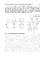
Fig. 9. (a) Schematic bottom view of multi-segment OLED device with and without metal-
dielectric AR. (b) Picture of such a device after fabrication. This device corresponds to the
design presented in Figure 8.
During theses optimizations, it was important to constrain the thickness values of organic
materials to ensure high efficiency OLEDs. For a similar reason, we introduced an Au layer
(which has a higher work function than Ag) to facilitate hole injection in the hole transport
layer (see Sec. 7). In addition, the thickness of the ITO film had to be large enough to form a
low resistivity anode and facilitate the contact with an external lead (although in some cases,
we found that the Au/Ag layer was thick enough so that no ITO layer was required).
Figures 7 and 8 show two different designs with a different number of layers in the metal-
dielectric AR part of the structure, along with their calculated performances (reflectance and
luminance spectra). The complex refractive index of all layers were measured from films
deposited in the same conditions as our devices. When compared to the performance of a
conventional OLED shown in Fig. 3(b) and (c), we see that the new designs reduce the
reflectance to 2% and less, which is 25 times less than that of a typical OLED, and that the
emission is of the same order of magnitude.
Figure 7(c) and 8(c) also show the distribution of the irradiance inside the OLEDs at the peak
wavelength. The maximum of irradiance at the position of the emitting layer indicates that a
microcavity effect occurs in the OLED. Not shown here is the fact that the optimization of
such designs with absorbing layers involves the adjustment of phase values φ
anode
and φ
cathode
in Eq. 3 (Poitras et al., 2003). In addition, the reduced irradiance values at positions
corresponding to the metal layers contribute to reduce the absorption of emitted light in
these layers (see Eq. 6).
Organic Light Emitting Diode138
6.2 Example of actual device
SiO
2
, TiO
2
and Inconel were deposited in a dual ion-beam sputtering deposition chamber
(Spector, Veeco-IonTech), and all other materials were thermally evaporated in a high-
vacuum cluster tool (Kurt J. Lesker), in separate chambers for metals and organics to avoid
cross-contamination and interface degradation. The complex refractive index spectra of
individual films were derived from measurements by ex-situ variable-angle spectroscopic
ellipsometer (VASE, J.A. Woollam Co.). These spectra were used to produce the final design
described and simulated in Figure 8.
The profile of the calculated irradiance, which is the light radiant flux per unit area, is
shown in Figure 1 at the peak wavelength of emission. The cavity is designed so that the
irradiance has a maximum in the Alq
3
layer at the NPB interface, where the emission
originates, and a minimum in the Ag/Au absorbing bilayer, where light absorption is
reduced. High contrast is obtained because the Au/Ag bilayer is highly absorbing seen from
the outside. Using published extinction coefficients for evaporated Au and Ag films (AIP,
1972), the transmittance of the Au/Ag bilayer without the cavity effect is calculated to be
0.042.
Actual devices were fabricated with the DBR materials sputtered through a shadow mask
on only half of a 2x2 in
2
glass slide to provide direct comparison between filtered and
unfiltered sides (see Figure 9). Ag and Au were evaporated through a shadow-mask to
define electrode tracks and an electrical separator lithographically patterned to define diode
segments (Roth et al., 2001). NPB, Alq
3
, Mg:Ag and a Ag capping layer were evaporated
with the contacts masked off. The samples were not encapsulated.
Reflectance measurements were performed using a spectrophotometer (Lambda-19, Perkin-
Elmer) equipped with a reflectance accessory (with an angle of incidence of 7°). The values
obtained (see Figure 10) are in qualitative agreement with our simulation, and show a very
clear improvement of the contrast. The spectral shift and discrepancy in values of reflectance
between simulated and measured spectra is due to the cumulative error in film thicknesses,
most probably from organic materials for which the control is less precise, but also from
variations in the optical constants of metallic films, which are critical.
The unfiltered OLED shows a deep absorption peak due to the Fabry-Perot resonance of the
naturally-occurring weak microcavity, and the filtered OLED shows oscillations in the
reflectance due to the same effect. Lower reflectance filters could be designed with more
layers in the DBR, at the expense of added complexity.
7. Conclusion
It is conceivable that future outdoor displays will combine different approaches: intensity
control, microstructure for light extraction, or displays based on reflection might be used,
but they will certainly include reflection-suppressing designs. As we saw earlier, efficiently
suppressing the light reflection from the device requires an integration of the antireflection
layers with the entire display device.
We have demonstrated the concept of a multilayer anode comprising an Au/Ag bilayer and
a metal-dielectric AR coating that has both a high internal reflectance and a low outside
reflectance. The former property is used to maintain a microcavity effect in the OLED that is
tuned to maximize light out-coupling, and the latter to improve the OLED contrast ratio.
Fig. 10. Theoretical and measured reflectance spectra, for OLED with and without integrated
metal-dielectric layers.
Further designs are being considered with varying thicknesses of the Au/Ag layer, and
fewer layers in the metal-dielectric coating for a simpler fabrication process.
Although the basic concepts described concerning the microcavity effect have been applied
in the present work to bottom-emission OLEDs and specific materials only, they are general
and will remain true whatever the materials used in the device (i.e. polymer-based), and for
other device structures (such as top-emitting-OLED, tandem-OLED, etc.).
The problem of contrast is complex: the optimum contrast for which a viewer is comfortable
depends on the color, and the surrounding light. For outside application, ideal solutions will
probably involve not only the reduction of the reflectance of the display, such as explained
here, but also the adjustment of display luminance and correction for the gamma parameter
(Poynton, 1993; Devlin et al., 2006).
Acknowledgments
The authors wish to thank Hiroshi Fukutani, Eric Estwick and Xiaoshu Tong for their
technical assistance. We also are grateful to Dr. Ye Tao for many fruitful discussions, and to
Prof. C.C. Lee.
Parts of this work were presented at the OSA 2007 Optical Interference Coating Conference
(Tucson, June 2007) and at the 13th Canadian Semiconductor Technology Conference
(Montreal, August 2007).
400 500 600 700 800
0
10
20
30
40
50
60
70
80
90
100
Reflectance (%)
Wavelength (nm)
Measured
Calculated
without metal/dielectric AR
with metal/dielectric AR
High-Contrast OLEDs with High-Efciency 139
6.2 Example of actual device
SiO
2
, TiO
2
and Inconel were deposited in a dual ion-beam sputtering deposition chamber
(Spector, Veeco-IonTech), and all other materials were thermally evaporated in a high-
vacuum cluster tool (Kurt J. Lesker), in separate chambers for metals and organics to avoid
cross-contamination and interface degradation. The complex refractive index spectra of
individual films were derived from measurements by ex-situ variable-angle spectroscopic
ellipsometer (VASE, J.A. Woollam Co.). These spectra were used to produce the final design
described and simulated in Figure 8.
The profile of the calculated irradiance, which is the light radiant flux per unit area, is
shown in Figure 1 at the peak wavelength of emission. The cavity is designed so that the
irradiance has a maximum in the Alq
3
layer at the NPB interface, where the emission
originates, and a minimum in the Ag/Au absorbing bilayer, where light absorption is
reduced. High contrast is obtained because the Au/Ag bilayer is highly absorbing seen from
the outside. Using published extinction coefficients for evaporated Au and Ag films (AIP,
1972), the transmittance of the Au/Ag bilayer without the cavity effect is calculated to be
0.042.
Actual devices were fabricated with the DBR materials sputtered through a shadow mask
on only half of a 2x2 in
2
glass slide to provide direct comparison between filtered and
unfiltered sides (see Figure 9). Ag and Au were evaporated through a shadow-mask to
define electrode tracks and an electrical separator lithographically patterned to define diode
segments (Roth et al., 2001). NPB, Alq
3
, Mg:Ag and a Ag capping layer were evaporated
with the contacts masked off. The samples were not encapsulated.
Reflectance measurements were performed using a spectrophotometer (Lambda-19, Perkin-
Elmer) equipped with a reflectance accessory (with an angle of incidence of 7°). The values
obtained (see Figure 10) are in qualitative agreement with our simulation, and show a very
clear improvement of the contrast. The spectral shift and discrepancy in values of reflectance
between simulated and measured spectra is due to the cumulative error in film thicknesses,
most probably from organic materials for which the control is less precise, but also from
variations in the optical constants of metallic films, which are critical.
The unfiltered OLED shows a deep absorption peak due to the Fabry-Perot resonance of the
naturally-occurring weak microcavity, and the filtered OLED shows oscillations in the
reflectance due to the same effect. Lower reflectance filters could be designed with more
layers in the DBR, at the expense of added complexity.
7. Conclusion
It is conceivable that future outdoor displays will combine different approaches: intensity
control, microstructure for light extraction, or displays based on reflection might be used,
but they will certainly include reflection-suppressing designs. As we saw earlier, efficiently
suppressing the light reflection from the device requires an integration of the antireflection
layers with the entire display device.
We have demonstrated the concept of a multilayer anode comprising an Au/Ag bilayer and
a metal-dielectric AR coating that has both a high internal reflectance and a low outside
reflectance. The former property is used to maintain a microcavity effect in the OLED that is
tuned to maximize light out-coupling, and the latter to improve the OLED contrast ratio.
Fig. 10. Theoretical and measured reflectance spectra, for OLED with and without integrated
metal-dielectric layers.
Further designs are being considered with varying thicknesses of the Au/Ag layer, and
fewer layers in the metal-dielectric coating for a simpler fabrication process.
Although the basic concepts described concerning the microcavity effect have been applied
in the present work to bottom-emission OLEDs and specific materials only, they are general
and will remain true whatever the materials used in the device (i.e. polymer-based), and for
other device structures (such as top-emitting-OLED, tandem-OLED, etc.).
The problem of contrast is complex: the optimum contrast for which a viewer is comfortable
depends on the color, and the surrounding light. For outside application, ideal solutions will
probably involve not only the reduction of the reflectance of the display, such as explained
here, but also the adjustment of display luminance and correction for the gamma parameter
(Poynton, 1993; Devlin et al., 2006).
Acknowledgments
The authors wish to thank Hiroshi Fukutani, Eric Estwick and Xiaoshu Tong for their
technical assistance. We also are grateful to Dr. Ye Tao for many fruitful discussions, and to
Prof. C.C. Lee.
Parts of this work were presented at the OSA 2007 Optical Interference Coating Conference
(Tucson, June 2007) and at the 13th Canadian Semiconductor Technology Conference
(Montreal, August 2007).
400 500 600 700 800
0
10
20
30
40
50
60
70
80
90
100
Reflectance (%)
Wavelength (nm)
Measured
Calculated
without metal/dielectric AR
with metal/dielectric AR
Organic Light Emitting Diode140
8. References
AIP (1972) American Institute of Physics Hanbook, Gray, D.E. ed. McGraw-Hill, 3
rd
edition,
ISBN 978-0070014855, New York.
Anderson, P. (2005). Advance Display Technologies, JISC Technology & Standards Watch
Report, August 2005. />
_techwatch/techwatch/techwatch_reports_0503.aspx
Aziz, H.; Liew, Y F.; Grandin, H. M. & Popovic, Z. D. (2003). Reduced reflectance cathode
for organic light-emitting devices using metalorganic mixtures, Appl. Phys. Lett.
Vol. 83, pp. 186—188.
Bahadur, B. (1991). Display parameters and requirements, In: Liquid Crystals: Applications and
Uses, B. Bahadur (Ed.), p. 82, World Scientific, ISBN 978-981-02-0111-1, Singapore.
Björk, G. (1991). Modification of spontaneous emission rate in planar dielectric microcavity
structures, Physical Review A, Vol. 44, No. 1, pp. 669—681.
Boff, K.R.; Lincoln, J.E. & Armstrong, H.G. (1988). Engineering Data Compendium. Vol.1.
Human Perception and Performance, Aerospace Medical Research Laboratory,
Wright-Patterson Air Force Base, ISBN 978-9992149201, Ohio.
Bulovic, V.; Khalfin, V.B; Gu, G.; Burrows, P.E.; Garbuzov, D.Z. & Forrest, S.R. (1998). Weak
microcavity effects in organic light-emitting devices, Phys. Rev. B. Vol. 58, No. 7,
p. 3730.
Devlin, K.; Chalmers, A. & Reinhard, E. (2006). Visual calibration and correction for ambient
illumination, ACM Transactions on Applied Perception. Vol. 3, No. 4, pp. 429—452.
Dobrowolski, J.A. (1981). Versatile computer program for absorbing optical thin film
systems, Appl. Opt. Vol. 20, pp. 74-81.
Dobrowolski, J.A.; Sullivan, B.T. & Bajcar, R.C. (1992). Optical interference, contrast-
enhanced electroluminescent device. Applied Optics, Vol. 31, No. 28, pp. 5988—5996,
ISSN 0003-6935.
Goos, F. (1937). Durchlässigkeit und reflexionsvermögen dünner silberschichten von
ultrarot bis ultraviolet, Zeitschrift für Physik A Hadrons and Nuclei. Vol. 106, No. 9—
10, pp. 606—619.
Jordan, R.H.; Rothberg, L.J.; Dodabalapur, A. & Slusher, R.E. (1996). “Efficiency-
enhancement of microcavity organic light-emitting diodes, Appl. Phys. Lett. Vol. 69,
No. 14, p. 1997.
Krasnov, A. N. (2002). High-contrast organic light-emitting diodes on flexible substrates,
Appl. Phys. Lett. Vol. 80, pp. 3853—3855.
Lemarquis, F. & Marchand, G. (1999). Analytical achromatic design of metal-dielectric
absorbers, Appl. Opt. Vol. 38, pp. 4876—4884.
Lee, G.J.; Jung, B. Y.; Hwangbo, C. K. & Yoon, J. S. (2002). Photoluminescence characteristics
in metal-distributed feedback-mirror microcavity containing luminescent polymer
and filler, Jpn. J. Appl. Phys. Vol. 41, p. 5241.
Macleod, H.A. (1978). A new approach in the design of metal-dielectric thin-film optical
coatings, Optica Acta. Vol. 25, No. 2, pp. 93—106.
Macleod, H.A. (2001). Thin-Film Optical Filters, Institute of Physics Publishing, ISBN
0750306882, Bristol.
Nuijs, A. M. & Horikx, J. J. L. (1994). Diffraction and scattering at antiglare structures for
display devices, Appl. Opt. Vol. 33, No. 18, pp. 4058—4068.
Palik, E. D. (1985). Handbook of Optical Constants of Solids, Vols. I and II, Academic Press,
ISBN 0125444222, New York.
Poitras, D.; Dalacu, D.; Liu, X.; Lefebvre, J.; Poole, P.J. & Williams, R. L. (2003). Luminescent
devices with symmetrical and asymmetrical microcavity structures, Proceedings of
the 46th Annual Tech. Conf. of Society of Vacuum Coaters, pp. 317—322, Philadelphia,
May 2003, ISSN 0737-5921, SVC Publication, Albuquerque.
Poynton, C.A. (1993). ‘Gamma’ and its Disguises: The Nonlinear Mappings of Intensity in
Perception, CRTs, Film and Video, SMPFTE Journal, Vol. 102, No. 12, pp. 1099—
1108.
Poynton, C.A. (2003). Digital video and HDTV – algorithms and interfaces, Morgan Kaufmann
Publisher, ISBN 1558607927, San Francisco.
Py, C.; Poitras, D.; Kuo, C C. & Fukutani, H. (2008). High-contrast Organic Light Emitting
Diodes with a partially absorbing anode, Opt. Lett. Vol. 33, No. 10, pp. 1126—1128.
Renault, O.; Salata, O. V.; Etchells, M.; Dobson, P. J. & Christou, V. (2000). A low reflectivity
multilayer cathode for organic light-emitting diodes, Thin Solid Films, Vol. 379, pp.
195—198.
Roth, D.; Py, C.; Fukutani, H.; Marshall, P.; Popela, M. & Leong, D. (2001). An Organic
Digital Integrated Multiplexing Clock Display, Presented at the 10th Canadian
Semiconductor Technology Conference, Ottawa, Canada, Aug 13—17.
Smith, S.D. (1958). Design of multilayer filters by considering two effective interfaces, J. Opt.
Soc. Am. Vol. 48, No. 1, pp. 43—50.
Tang, C.W. & VanSlyke, S.A. (1987) Organic electroluminescent diodes, Appl. Phys. Lett. Vol.
51, No. 11, pp. 913 915.
Trapani, G.; Pawlak, R.; Carlson, G. R. & Gordon, J. N. (2003). High durability circular
polarizer for use with emissive displays, US Patent 6549335.
Uriba, T.; Yamada, J.; Sasaoka, T. (2004) Display and method of manufacturing the same,
US Patent 2004/0147200A1.
Wu, C C.; Chen, C W.; Lin, C L. & Yang, C J. (2005) Advanced Organic Light-Emitting
Devices for Enhancing Display Performances, J. Display Technol. Vol. 1, No. 2,
pp. 248—266.
Wyszecki, G. (1968). Recent Agreements Reached by the Colorimetry Committee of the
Commission Internationale de l'Eclairage (abstract). , J. Opt. Soc. Am. Vol. 58, No. 2,
pp. 290—292.
WVASE32 software (J.A. Woollam Co., Lincolrn NE)
High-Contrast OLEDs with High-Efciency 141
8. References
AIP (1972) American Institute of Physics Hanbook, Gray, D.E. ed. McGraw-Hill, 3
rd
edition,
ISBN 978-0070014855, New York.
Anderson, P. (2005). Advance Display Technologies, JISC Technology & Standards Watch
Report, August 2005.
_techwatch/techwatch/techwatch_reports_0503.aspx
Aziz, H.; Liew, Y F.; Grandin, H. M. & Popovic, Z. D. (2003). Reduced reflectance cathode
for organic light-emitting devices using metalorganic mixtures, Appl. Phys. Lett.
Vol. 83, pp. 186—188.
Bahadur, B. (1991). Display parameters and requirements, In: Liquid Crystals: Applications and
Uses, B. Bahadur (Ed.), p. 82, World Scientific, ISBN 978-981-02-0111-1, Singapore.
Björk, G. (1991). Modification of spontaneous emission rate in planar dielectric microcavity
structures, Physical Review A, Vol. 44, No. 1, pp. 669—681.
Boff, K.R.; Lincoln, J.E. & Armstrong, H.G. (1988). Engineering Data Compendium. Vol.1.
Human Perception and Performance, Aerospace Medical Research Laboratory,
Wright-Patterson Air Force Base, ISBN 978-9992149201, Ohio.
Bulovic, V.; Khalfin, V.B; Gu, G.; Burrows, P.E.; Garbuzov, D.Z. & Forrest, S.R. (1998). Weak
microcavity effects in organic light-emitting devices, Phys. Rev. B. Vol. 58, No. 7,
p. 3730.
Devlin, K.; Chalmers, A. & Reinhard, E. (2006). Visual calibration and correction for ambient
illumination, ACM Transactions on Applied Perception. Vol. 3, No. 4, pp. 429—452.
Dobrowolski, J.A. (1981). Versatile computer program for absorbing optical thin film
systems, Appl. Opt. Vol. 20, pp. 74-81.
Dobrowolski, J.A.; Sullivan, B.T. & Bajcar, R.C. (1992). Optical interference, contrast-
enhanced electroluminescent device. Applied Optics, Vol. 31, No. 28, pp. 5988—5996,
ISSN 0003-6935.
Goos, F. (1937). Durchlässigkeit und reflexionsvermögen dünner silberschichten von
ultrarot bis ultraviolet, Zeitschrift für Physik A Hadrons and Nuclei. Vol. 106, No. 9—
10, pp. 606—619.
Jordan, R.H.; Rothberg, L.J.; Dodabalapur, A. & Slusher, R.E. (1996). “Efficiency-
enhancement of microcavity organic light-emitting diodes, Appl. Phys. Lett. Vol. 69,
No. 14, p. 1997.
Krasnov, A. N. (2002). High-contrast organic light-emitting diodes on flexible substrates,
Appl. Phys. Lett. Vol. 80, pp. 3853—3855.
Lemarquis, F. & Marchand, G. (1999). Analytical achromatic design of metal-dielectric
absorbers, Appl. Opt. Vol. 38, pp. 4876—4884.
Lee, G.J.; Jung, B. Y.; Hwangbo, C. K. & Yoon, J. S. (2002). Photoluminescence characteristics
in metal-distributed feedback-mirror microcavity containing luminescent polymer
and filler, Jpn. J. Appl. Phys. Vol. 41, p. 5241.
Macleod, H.A. (1978). A new approach in the design of metal-dielectric thin-film optical
coatings, Optica Acta. Vol. 25, No. 2, pp. 93—106.
Macleod, H.A. (2001). Thin-Film Optical Filters, Institute of Physics Publishing, ISBN
0750306882, Bristol.
Nuijs, A. M. & Horikx, J. J. L. (1994). Diffraction and scattering at antiglare structures for
display devices, Appl. Opt. Vol. 33, No. 18, pp. 4058—4068.
Palik, E. D. (1985). Handbook of Optical Constants of Solids, Vols. I and II, Academic Press,
ISBN 0125444222, New York.
Poitras, D.; Dalacu, D.; Liu, X.; Lefebvre, J.; Poole, P.J. & Williams, R. L. (2003). Luminescent
devices with symmetrical and asymmetrical microcavity structures, Proceedings of
the 46th Annual Tech. Conf. of Society of Vacuum Coaters, pp. 317—322, Philadelphia,
May 2003, ISSN 0737-5921, SVC Publication, Albuquerque.
Poynton, C.A. (1993). ‘Gamma’ and its Disguises: The Nonlinear Mappings of Intensity in
Perception, CRTs, Film and Video, SMPFTE Journal, Vol. 102, No. 12, pp. 1099—
1108.
Poynton, C.A. (2003). Digital video and HDTV – algorithms and interfaces, Morgan Kaufmann
Publisher, ISBN 1558607927, San Francisco.
Py, C.; Poitras, D.; Kuo, C C. & Fukutani, H. (2008). High-contrast Organic Light Emitting
Diodes with a partially absorbing anode, Opt. Lett. Vol. 33, No. 10, pp. 1126—1128.
Renault, O.; Salata, O. V.; Etchells, M.; Dobson, P. J. & Christou, V. (2000). A low reflectivity
multilayer cathode for organic light-emitting diodes, Thin Solid Films, Vol. 379, pp.
195—198.
Roth, D.; Py, C.; Fukutani, H.; Marshall, P.; Popela, M. & Leong, D. (2001). An Organic
Digital Integrated Multiplexing Clock Display, Presented at the 10th Canadian
Semiconductor Technology Conference, Ottawa, Canada, Aug 13—17.
Smith, S.D. (1958). Design of multilayer filters by considering two effective interfaces, J. Opt.
Soc. Am. Vol. 48, No. 1, pp. 43—50.
Tang, C.W. & VanSlyke, S.A. (1987) Organic electroluminescent diodes, Appl. Phys. Lett. Vol.
51, No. 11, pp. 913 915.
Trapani, G.; Pawlak, R.; Carlson, G. R. & Gordon, J. N. (2003). High durability circular
polarizer for use with emissive displays, US Patent 6549335.
Uriba, T.; Yamada, J.; Sasaoka, T. (2004) Display and method of manufacturing the same,
US Patent 2004/0147200A1.
Wu, C C.; Chen, C W.; Lin, C L. & Yang, C J. (2005) Advanced Organic Light-Emitting
Devices for Enhancing Display Performances, J. Display Technol. Vol. 1, No. 2,
pp. 248—266.
Wyszecki, G. (1968). Recent Agreements Reached by the Colorimetry Committee of the
Commission Internationale de l'Eclairage (abstract). , J. Opt. Soc. Am. Vol. 58, No. 2,
pp. 290—292.
WVASE32 software (J.A. Woollam Co., Lincolrn NE)
Organic Light Emitting Diode142
Optimum Structure Adjustment for Flexible
Fluorescent and Phosphorescent Organic Light Emitting Diodes 143
Optimum Structure Adjustment for Flexible Fluorescent and
Phosphorescent Organic Light Emitting Diodes
Fuh-Shyang Juang, Yu-Sheng Tsai, Shun-Hsi Wang, Shin-Yuan Su, Shin-Liang Chen and
Shen-Yaur Chen
X
Optimum Structure Adjustment for Flexible
Fluorescent and Phosphorescent Organic
Light Emitting Diodes
Fuh-Shyang Juang, Yu-Sheng Tsai, Shun-Hsi Wang,
Shin-Yuan Su, Shin-Liang Chen and Shen-Yaur Chen
National Formosa University
Taiwan
1. Introduction
The organic light emitting diodes (OLEDs) [1] is a new-generation flat panel display with
the advantages of self-luminescence, wide viewing angle (> 160°), prompt response time (~1
μs), low operating voltage (3~10 V), high luminance efficiency, high color purity, and easy
to be made on various substrates. Therefore, it’s an important topic that how to improve the
luminance efficiency, lifetime and the adhesion characters of ITO/organic interface of
flexible OLEDs. Zugang Liu et al. reported that the NPB (HTL) is suitable in contact with the
emission layer and when they form an energy ladder structure, the driving voltage
decreased and the electroluminescent output increased [2]. Thus it can be seen, the hole
transport layer [3-6] is very important to balance the injection of hole and electron, to
increase the luminance efficiency and lifetime. In recent years, the hole buffer layer of device
typically employs LiF [7], CuPc [8], Pani:PSS [9-10] or PEDOT:PSS [9-11] to improve the hole
injection efficiency. In addition, a flexible substrate (PET, metal foil, etc.) surface is not
completely smooth and will usually have spikes. After the organic thin film evaporates onto
the ITO substrate surface the spikes will still exist. When the device is operated under high
voltage or high current density, a heavy amount of electric current will concentrate at the
spikes and damage the device by causing the device to short circuit, creating Joule heat. The
luminance efficiency of the device will therefore be reduced producing shorter device
lifetime. Thus, the PEDOT:PSS fabrication process uses spin-coating to obtain a thin film
with a smoother surface than that produced by thermal deposition. Spin-coating enhances
the organic material adhesion in subsequent processes, thereby directly affecting the
performance of flexible OLED. For the above reason, this research dissolved hole transport
material N,N’-diphenyl-N,N’-bis(1-naphthyl)- 1,1’biphenyl-4,4’’diamine (α-NPD), N,N’-
Bis(naphthalene- l-yl) -N,N’-bis(phenyl)-benzidine (NPB) or α-NPD:NPB in tetrahydrfuran
(THF) solvent and spin-coated the buffer layer onto ITO surface of flexible OLEDs.
Phosphorescent dye gains energy from the radiative recombination of both singlet and
triplet excitons [12], improving the internal quantum efficiency of fluorescent OLEDs
(FOLEDs) typically 25% at maximum to nearly 100% [13]. Enhancing the luminance
8
Organic Light Emitting Diode144
efficiency of phosphorescent OLED has attracted the interest of many researchers.
Improving device efficiency, the triplet state excitons must be confined in the emitting layer
to increase the chance for energy transfer from host to guest. The material that achieves this
effect is called the hole blocking layer (HBL), CF-X [14], CF-Y [14], BCP [12], TPBi [15], and
BAlq [16]. These materials have higher ionization energy and band gap that can block the
diffusion of excitons. When the host-guest orbit overlap is weak, the blocking layer action is
particularly important.
2. Experiment
The ITO substrate used in this study was 80Ω/□ PET substrate. Before depositing the
patterned ITO substrate was placed in O
2
plasma for surface cleaning. The spin-coating
solvents were then prepared by dissolving hole transport materials N,N’-diphenyl-N,N’-
bis(1-naphthyl)- 1,1’biphenyl-4,4’’diamine (α-NPD) and N,N’-Bis(naphthalene-l-yl) -N,N’-
bis(phenyl)-benzidine (NPB) (α-NPD mixed NPB with 1:1 wt%) in tetrahydrfuran (THF)
solvent. The chemicals are vibrated ultrasonically in solution for 60 minutes to facilitate the
dissolving process. The coating process is then carried out for 35 seconds at 4500 r.p.m. to
deposit the buffer layer onto the ITO surface. After that the substrate was placed in an
organic evaporation chamber to deposit the organic layers under 2×10
-6
torr, α-NPD or NPB
was deposited as hole transport layer (HTL), 4,4'-Bis(carbazol-9-yl) biphenyl (CBP) was
deposited as the phosphorescent device host, Tris(2-pheny-lpyridine) iridium(III) (Ir(ppy)
3
)
was deposited as the phosphorescent device guest material, 2,9-Dime-thyl-4,7-diphenyl-
1,10-phenanhroline (BCP) or 2,2',2''-(1,3,5-Benzinetriyl) -tris(1-phenyl-1-H-benzimidazole)
(TPBi) was deposited as the hole blocking layer (HBL), Tris(8-hydroxy-
quinolinato)aluminum (Alq3) was deposited as emitting layer (EML) of fluorescent and
electron transport layer (ETL), and 1,3-Bis[2-(2,2'-bipyridine-6-yl)-1,3,4-oxadiazo-5-
yl]benzene (Bpy-OXD) was deposited as electron transport layer/ hole blocking layer. The
chemical structures of all used organic materials are shown in Fig. 1. SpectraScan PR650 and
Keithley 2400 equipment were employed to measure the luminance and current-voltage
characteristics.
(a) (b) (c)
(d) (e) (f)
(g) (h)
Fig. 1. The chemical structures of all used organic materials (a) NPB, (b) α-NPD, (c) CBP, (d)
Ir(ppy)
3
, (e) BCP, (f) TPBi, (g) Alq3 and (h) Bpy-OXD
3. Results and discussion
3.1 Optimum Structure Adjustment for Flexible Phosphorescent Organic Light
Emitting Diodes
NO.
Sub.
ITO NPB
Dopant 7% Ir(ppy)
3
in CBP
HBL
Alq3LiFAl
A1
Plastic
(PET)
ITO
(80/)
40
20
BCP
0
40
0.5
65
A2
BCP
5
A3
BCP
10*
A4
BCP
15
B1
30
20
BCP
10
40
A3
40
B2
50*
B3
70
C1
50
20
BCP
10
30
B2
40
C2
50*
C3
70
D1
50
10
BCP
10
50
C2
20
D2
30
D3
40*
E1
50
40
TPBi
5
50 E2
TPBi
10*
E3
TPBi
15
*optimum parameters
Table 1. Adjustment parameters of Phosphorescent organic light emitting diodes (unit: nm)
Optimum Structure Adjustment for Flexible
Fluorescent and Phosphorescent Organic Light Emitting Diodes 145
efficiency of phosphorescent OLED has attracted the interest of many researchers.
Improving device efficiency, the triplet state excitons must be confined in the emitting layer
to increase the chance for energy transfer from host to guest. The material that achieves this
effect is called the hole blocking layer (HBL), CF-X [14], CF-Y [14], BCP [12], TPBi [15], and
BAlq [16]. These materials have higher ionization energy and band gap that can block the
diffusion of excitons. When the host-guest orbit overlap is weak, the blocking layer action is
particularly important.
2. Experiment
The ITO substrate used in this study was 80Ω/□ PET substrate. Before depositing the
patterned ITO substrate was placed in O
2
plasma for surface cleaning. The spin-coating
solvents were then prepared by dissolving hole transport materials N,N’-diphenyl-N,N’-
bis(1-naphthyl)- 1,1’biphenyl-4,4’’diamine (α-NPD) and N,N’-Bis(naphthalene-l-yl) -N,N’-
bis(phenyl)-benzidine (NPB) (α-NPD mixed NPB with 1:1 wt%) in tetrahydrfuran (THF)
solvent. The chemicals are vibrated ultrasonically in solution for 60 minutes to facilitate the
dissolving process. The coating process is then carried out for 35 seconds at 4500 r.p.m. to
deposit the buffer layer onto the ITO surface. After that the substrate was placed in an
organic evaporation chamber to deposit the organic layers under 2×10
-6
torr, α-NPD or NPB
was deposited as hole transport layer (HTL), 4,4'-Bis(carbazol-9-yl) biphenyl (CBP) was
deposited as the phosphorescent device host, Tris(2-pheny-lpyridine) iridium(III) (Ir(ppy)
3
)
was deposited as the phosphorescent device guest material, 2,9-Dime-thyl-4,7-diphenyl-
1,10-phenanhroline (BCP) or 2,2',2''-(1,3,5-Benzinetriyl) -tris(1-phenyl-1-H-benzimidazole)
(TPBi) was deposited as the hole blocking layer (HBL), Tris(8-hydroxy-
quinolinato)aluminum (Alq3) was deposited as emitting layer (EML) of fluorescent and
electron transport layer (ETL), and 1,3-Bis[2-(2,2'-bipyridine-6-yl)-1,3,4-oxadiazo-5-
yl]benzene (Bpy-OXD) was deposited as electron transport layer/ hole blocking layer. The
chemical structures of all used organic materials are shown in Fig. 1. SpectraScan PR650 and
Keithley 2400 equipment were employed to measure the luminance and current-voltage
characteristics.
(a) (b) (c)
(d) (e) (f)
(g) (h)
Fig. 1. The chemical structures of all used organic materials (a) NPB, (b) α-NPD, (c) CBP, (d)
Ir(ppy)
3
, (e) BCP, (f) TPBi, (g) Alq3 and (h) Bpy-OXD
3. Results and discussion
3.1 Optimum Structure Adjustment for Flexible Phosphorescent Organic Light
Emitting Diodes
NO.
Sub.
ITO NPB
Dopant 7% Ir(ppy)
3
in CBP
HBL
Alq3LiFAl
A1
Plastic
(PET)
ITO
(80/)
40
20
BCP
0
40
0.5
65
A2
BCP
5
A3
BCP
10*
A4
BCP
15
B1
30
20
BCP
10
40
A3
40
B2
50*
B3
70
C1
50
20
BCP
10
30
B2
40
C2
50*
C3
70
D1
50
10
BCP
10
50
C2
20
D2
30
D3
40*
E1
50
40
TPBi
5
50 E2
TPBi
10*
E3
TPBi
15
*optimum parameters
Table 1. Adjustment parameters of Phosphorescent organic light emitting diodes (unit: nm)
Organic Light Emitting Diode146
In this study the device structures are shown in Table 1. First, we inserted a hole blocking
layer (HBL) to effectively confine the holes in the emitting layer (EML) for improving the
luminance efficiency of the devices. Moreover, varied the thickness of BCP from 0 to 15 nm;
it was found that the best hole-blocking result was present at 10 nm of the thickness of BCP
(as shown in Fig.1). However, if the thickness of BCP was increased to 15 nm, the hole
blocking result was better, but the distance of injecting electrons to EML was increased and
caused the brightness decreased. Then, we tried to vary the thickness of NPB to make the
amount of the hole injected into EML match with the amount of the electron for increasing
the luminance efficiency of the device. From Fig. 2, it was found that the maximum
luminance efficiency of the device can be obtained at 50 nm of the thickness of NPB.
Furthermore, we varied the thickness of Alq3 to make the amount of the electron injected
into EML match with the amount of the hole. From Fig. 3, it was found that the maximum
luminance efficiency of the device can be obtained at 50 nm of the thickness of Alq3.
However, if the thickness of Alq3 was increased to 70 nm, the distance of the electron
injecting to EML was enhanced to decrease the amount of the electron injected into the EML
to cause the brightness greatly decreased. At last, we varied the thickness of the EML of
CBP:Ir(ppy)3 from 10 nm to 40 nm and hoped that the chance of recombining electron-hole
will be increased via varying the thickness of the EML to increase the brightness and
luminance efficiency. From the experiment result, it was found that the best luminance
efficiency would be obtained at the layer thickness of 40 nm (as shown in Fig. 4); at the
moment, the device efficiency was greatly increased to 30.4 cd/A.
0 20 40 60
Curren
t
Densi
t
y
(
m
A
/
cm
2
)
0
3
6
9
12
15
18
21
2
4
Yield (cd
/
A)
BCP-10nm
BCP-15nm
BCP-5nm
BCP-0nm
Fig. 1. Luminance efficiency-current density curves for different thicknesses of HBL
0 2 4 6 8 10
Current Densit
y
(
m
A
/
cm
2
)
9
12
15
18
21
24
27
30
Yield (cd/A)
NPB-70nm
NPB-50nm
NPB-40nm
NPB-30nm
Fig. 2. Luminance efficiency-current density curves for different thicknesses of HTL
0 5 10 15 20 25 30
Curren
t
Densi
t
y
(
m
A
/
cm
2
)
5
10
15
20
25
30
Yield (cd/A)
Alq3-70nm
Alq3-50nm
Alq3-40nm
Alq3-30nm
Fig. 3. Luminance efficiency-current density curves for different thicknesses of ETL
Optimum Structure Adjustment for Flexible
Fluorescent and Phosphorescent Organic Light Emitting Diodes 147
In this study the device structures are shown in Table 1. First, we inserted a hole blocking
layer (HBL) to effectively confine the holes in the emitting layer (EML) for improving the
luminance efficiency of the devices. Moreover, varied the thickness of BCP from 0 to 15 nm;
it was found that the best hole-blocking result was present at 10 nm of the thickness of BCP
(as shown in Fig.1). However, if the thickness of BCP was increased to 15 nm, the hole
blocking result was better, but the distance of injecting electrons to EML was increased and
caused the brightness decreased. Then, we tried to vary the thickness of NPB to make the
amount of the hole injected into EML match with the amount of the electron for increasing
the luminance efficiency of the device. From Fig. 2, it was found that the maximum
luminance efficiency of the device can be obtained at 50 nm of the thickness of NPB.
Furthermore, we varied the thickness of Alq3 to make the amount of the electron injected
into EML match with the amount of the hole. From Fig. 3, it was found that the maximum
luminance efficiency of the device can be obtained at 50 nm of the thickness of Alq3.
However, if the thickness of Alq3 was increased to 70 nm, the distance of the electron
injecting to EML was enhanced to decrease the amount of the electron injected into the EML
to cause the brightness greatly decreased. At last, we varied the thickness of the EML of
CBP:Ir(ppy)3 from 10 nm to 40 nm and hoped that the chance of recombining electron-hole
will be increased via varying the thickness of the EML to increase the brightness and
luminance efficiency. From the experiment result, it was found that the best luminance
efficiency would be obtained at the layer thickness of 40 nm (as shown in Fig. 4); at the
moment, the device efficiency was greatly increased to 30.4 cd/A.
0 20 40 60
Curren
t
Densi
t
y
(
m
A
/
cm
2
)
0
3
6
9
12
15
18
21
2
4
Yield (cd
/
A)
BCP-10nm
BCP-15nm
BCP-5nm
BCP-0nm
Fig. 1. Luminance efficiency-current density curves for different thicknesses of HBL
0 2 4 6 8 10
Current Densit
y
(
m
A
/
cm
2
)
9
12
15
18
21
24
27
30
Yield (cd/A)
NPB-70nm
NPB-50nm
NPB-40nm
NPB-30nm
Fig. 2. Luminance efficiency-current density curves for different thicknesses of HTL
0 5 10 15 20 25 30
Curren
t
Densi
t
y
(
m
A
/
cm
2
)
5
10
15
20
25
30
Yield (cd/A)
Alq3-70nm
Alq3-50nm
Alq3-40nm
Alq3-30nm
Fig. 3. Luminance efficiency-current density curves for different thicknesses of ETL
Organic Light Emitting Diode148
0 5 10 15 20 25 30
Current Densit
y
(
m
A
/
cm
2
)
0
5
10
15
20
25
30
Yield (cd/A)
CBP:7%Ir(ppy)
3
-40nm
CBP:7%Ir(ppy)
3
-30nm
CBP:7%Ir(ppy)
3
-20nm
CBP:7%Ir(ppy)
3
-10nm
Fig. 4. Luminance efficiency-current density curves for different thicknesses of EML
Finally the doping concentration of (Ir(ppy)
3
) was adjusted as shown in Table 2. We found
in Fig. 5 that when the doping concentration was 7 wt% the device has optimum luminance
efficiency. In this study we also changed different hole blocking layers (HBL) BCP and TPBi,
whose structures are shown in Table 1, respectively. It is found from luminance efficiency -
current density in Fig. 5 that using TPBi as hole blocking layer could enhance the luminance
efficiency further to 34.2 cd/A. This is because the HOMO of TPBi (6.7 eV) is higher than the
HOMO of BCP (6.3 eV), which confines holes and excitons in the emitting layer more
effectively and prevents direct diffusion of holes or excitons to Alq3 layer. After comparing
the effects of different HBLs on luminance efficiency as shown in Fig. 5, it is found a suitable
material of HBL can improve the luminance efficiency of device effectively.
From the results of these serial experiments, it is found that whenever the thickness of an
organic layer has been adjusted, the luminance efficiency of the device has increased (as
shown in Fig. 6). It is because the amount of electron-hole of the device becomes more
balanced via the optimization of the hole transport layer and the electron transport layer. In
addition, extending the charge carrier recombining area and using more suitable HBL
material and suitable thickness of its thin film will gradually increase and improve the
luminance efficiency of the device.
NO. Sub. ITO NPB
Ir(ppy)
3
:CBP
HBL
Alq3
LiF Al
concen
.
thickness
F1
Plastic
(PET)
ITO
(80/)
50
4%
40
BCP
10
50 0.5 65
D3 7%*
F2 8%
F3 10%
*optimum parameters
Table 2. Adjustment parameters of PHOLEDs with different Ir(ppy)
3
doping concentrations
(unit: nm)
0 3 6 9 12 15 18 21 24 27
Current Densit
y
(
m
A
/
cm
2
)
15
18
21
24
27
30
33
36
Yield (cd/A)
CBP:7%Ir(ppy)
3
/ /TPBi 10nm
CBP:4%Ir(ppy)
3
/ /BCP 10nm
CBP:7%Ir(ppy)
3
/ /BCP 10nm
CBP:8%Ir(ppy)
3
/ /BCP 10nm
CBP:10%Ir(ppy)
3
/ /BCP 10nm
Fig. 5. Luminance efficiency-current density curves of PHOLEDs with different Ir(ppy)
3
doping concentrations and HBL materials
0 10 20 30 40 50
Current Densit
y
(
m
A
/
cm
2
)
10
15
20
25
30
3
5
Yield (cd
/
A)
TPBi(10nm)
EML(40nm)
Alq3(50nm)
NPB(50nm)
BCP(10nm)
optimum for each
adjusted group
Fig. 6. Luminance efficiency-current density of optimum thickness for each adjusted layer
3.2 Spin-coating (α-NPD:NPB)+THF as the buffer layer and evaporating NPB as the
hole transport layer to improve fluorescent OLED characteristics
Because the spin-coating rotation speed directly affects the film thickness, we fixed the spin-
coating time at 35 seconds from the beginning of the experiment. The rotation speed of the
spinα-NPD:NPB layer (3500, 4000, 4500 and 5000 r.p.m.) was varied to study how the device
optoelectronic characteristic was affected by the rotation speed of spin-coating. The device
structure was PET/ ITO (160 nm)/spin-coated (NPB:α-NPD)+THF (different rotation
speed)/evaporated NPB (41 nm)/Alq3 (52 nm)/Bpy-OXD (15 nm)/LiF (0.5 nm)/Al (135
nm). The device energy band structure was shown in Figs. 7(a). Because the coated film
Optimum Structure Adjustment for Flexible
Fluorescent and Phosphorescent Organic Light Emitting Diodes 149
0 5 10 15 20 25 30
Current Densit
y
(
m
A
/
cm
2
)
0
5
10
15
20
25
30
Yield (cd/A)
CBP:7%Ir(ppy)
3
-40nm
CBP:7%Ir(ppy)
3
-30nm
CBP:7%Ir(ppy)
3
-20nm
CBP:7%Ir(ppy)
3
-10nm
Fig. 4. Luminance efficiency-current density curves for different thicknesses of EML
Finally the doping concentration of (Ir(ppy)
3
) was adjusted as shown in Table 2. We found
in Fig. 5 that when the doping concentration was 7 wt% the device has optimum luminance
efficiency. In this study we also changed different hole blocking layers (HBL) BCP and TPBi,
whose structures are shown in Table 1, respectively. It is found from luminance efficiency -
current density in Fig. 5 that using TPBi as hole blocking layer could enhance the luminance
efficiency further to 34.2 cd/A. This is because the HOMO of TPBi (6.7 eV) is higher than the
HOMO of BCP (6.3 eV), which confines holes and excitons in the emitting layer more
effectively and prevents direct diffusion of holes or excitons to Alq3 layer. After comparing
the effects of different HBLs on luminance efficiency as shown in Fig. 5, it is found a suitable
material of HBL can improve the luminance efficiency of device effectively.
From the results of these serial experiments, it is found that whenever the thickness of an
organic layer has been adjusted, the luminance efficiency of the device has increased (as
shown in Fig. 6). It is because the amount of electron-hole of the device becomes more
balanced via the optimization of the hole transport layer and the electron transport layer. In
addition, extending the charge carrier recombining area and using more suitable HBL
material and suitable thickness of its thin film will gradually increase and improve the
luminance efficiency of the device.
NO. Sub. ITO NPB
Ir(ppy)
3
:CBP
HBL
Alq3
LiF Al
concen
.
thickness
F1
Plastic
(PET)
ITO
(80/)
50
4%
40
BCP
10
50 0.5 65
D3 7%*
F2 8%
F3 10%
*optimum parameters
Table 2. Adjustment parameters of PHOLEDs with different Ir(ppy)
3
doping concentrations
(unit: nm)
0 3 6 9 12 15 18 21 24 27
Current Densit
y
(
m
A
/
cm
2
)
15
18
21
24
27
30
33
36
Yield (cd/A)
CBP:7%Ir(ppy)
3
/ /TPBi 10nm
CBP:4%Ir(ppy)
3
/ /BCP 10nm
CBP:7%Ir(ppy)
3
/ /BCP 10nm
CBP:8%Ir(ppy)
3
/ /BCP 10nm
CBP:10%Ir(ppy)
3
/ /BCP 10nm
Fig. 5. Luminance efficiency-current density curves of PHOLEDs with different Ir(ppy)
3
doping concentrations and HBL materials
0 10 20 30 40 50
Current Densit
y
(
m
A
/
cm
2
)
10
15
20
25
30
3
5
Yield (cd
/
A)
TPBi(10nm)
EML(40nm)
Alq3(50nm)
NPB(50nm)
BCP(10nm)
optimum for each
adjusted group
Fig. 6. Luminance efficiency-current density of optimum thickness for each adjusted layer
3.2 Spin-coating (α-NPD:NPB)+THF as the buffer layer and evaporating NPB as the
hole transport layer to improve fluorescent OLED characteristics
Because the spin-coating rotation speed directly affects the film thickness, we fixed the spin-
coating time at 35 seconds from the beginning of the experiment. The rotation speed of the
spinα-NPD:NPB layer (3500, 4000, 4500 and 5000 r.p.m.) was varied to study how the device
optoelectronic characteristic was affected by the rotation speed of spin-coating. The device
structure was PET/ ITO (160 nm)/spin-coated (NPB:α-NPD)+THF (different rotation
speed)/evaporated NPB (41 nm)/Alq3 (52 nm)/Bpy-OXD (15 nm)/LiF (0.5 nm)/Al (135
nm). The device energy band structure was shown in Figs. 7(a). Because the coated film
Organic Light Emitting Diode150
thickness will become thick under lower rotation speed, from Fig. 7(b), we can see the
lowest current density flowing through the device at the lowest rotation speed (3500 r.p.m.).
According to the Mott-Gurney rule [17], we know that the current density presents an
inverse-proportion relation with the thickness, and the greatest NPB spin-coating layer
thickness can be estimated to appear at a rotation speed of 3500 r.p.m. However, the layer
thickness will become thinner as the rotation speed increases and the current density will
increase accordingly. However, at 5000 r.p.m., we found that the device current density
decreased. The major reason results from too high rotation speed which causes the
centrifugal force to become too strong, preventing the NPB+THF solution from attaching
onto the ITO surface; hence, the film thickness becomes uneven. From Fig. 8 luminance-
current density characteristic curve, we can observe the same trend in the current density-
voltage curve. Hence, we determined that 4500 r.p.m. is the optimal spin-coating parameter
to get the best optoelectronic characteristic.
Alq3
5.7eV
3.1eV
ITO
4.7eV
spin
NPB:
α
-NPD
5.6eV
2.5eV
5.3eV
2.1eV
evap.
NPB
5.3eV
2.1eV
Bpy-
OXD
2.92eV
6.56eV
Al
4.2eV
LiF
Alq3
5.7eV
3.1eV
Alq3
5.7eV
3.1eV
ITO
4.7eV
spin
NPB:
α
-NPD
5.6eV
2.5eV
5.3eV
2.1eV
spin
NPB:
α
-NPD
5.6eV
2.5eV
5.3eV
2.1eV
evap.
NPB
5.3eV
2.1eV
evap.
NPB
5.3eV
2.1eV
Bpy-
OXD
2.92eV
6.56eV
Bpy-
OXD
2.92eV
6.56eV
Al
4.2eV
AlAl
4.2eV
LiFLiF
0 2 4 6 8 1 0
V
olta
g
e
(
volt
)
0
40
80
12 0
16 0
Current Density (mA/cm
2
)
spin NPB:
-NPD/NPB(41)Alq3(52)/Bpy-OXD(15)
5000 r.p.m.
4500 r.p.m.
4000 r.p.m.
3500 r.p.m.
`
(a) (b)
Fig. 7. (a) The energy band structure of the device with spin-coating (NPB:α-NPD)+THF
buffer layer; (b) J–V characteristics for different rotation speeds
0 2 4 6 8 1 0
V
o
lta
g
e
(
v
o
lt
)
0
1000
2000
3000
4000
5000
Lu
m
in
a
n
c
e (
c
d
/
m
2
)
spin (NPB:
-NPD)+THF
/NPB(41)/Alq3(52)/Bpy-OXD(15)
5000 rpm
4500 rpm
4000 rpm
3500 rpm
Fig. 8. L–V characteristics for spino-coating (NPB:α-NPD)+THF with different rotation
speeds
To further verify the first HTL (NPB:α-NPD)+THF manufacturing process versus improving
the device optoelectronic characteristics, the following experiment was conducted. Devices
with PET/ITO(160 nm)/ HTL/Alq3(52 nm)/Bpy-OXD(15 nm)/LiF(0.5 nm)/Al(135 nm)
structures wherein the HTL was produced via the spin-coating or thermal-evaporation
process or both, are shown in Table 3.
Under same current density, the optoelectronic characteristics of Devices G1 and G2
(employing both spin-coated and evaporated double HTLs structures) were higher than that
of traditional devices made with single HTL using only thermal-evaporation (Device G3), as
shown in Fig. 9(a) and 9(b). The device characteristics with double HTLs were also found
better than those with the single HTL spin-coated structure (NPB:α-NPD)+THF only (Device
G4). Because spin-coating the film in the amorphous mode on the ITO surface does not
easily generate pin holes, and the organic layer contact with the ITO becomes tighter, the
HTL surface roughness can be greatly improved [18-21]. Therefore, the holes are injected
more easily from the ITO electrode into the NPB layer. Furthermore, the optoelectronic
characteristics of Device G1 were better than Device G2 because spin-coating (NPB:α-
NPD)+THF has similar p-type doping properties that enable holes to be injected efficiently
[22]. NPB and α-NPD co-doping will produce band bending and enable the holes to tunnel
from the ITO electrode into the HTL, forming an Ohmic contact interface [23]. Consequently
the Device G1 exhibited the best performances than the other devices. Fourier Transform
Infrared Spectroscopy (FTIR) was also performed on the HTL films to study the variation in
molecular structure. Moreover, from the lifetime test results shown in Fig. 10, the lifetime of
Device G1 was the longest, increased by about 41 % longer than Device G3 (fabricated
without spin-coating (NPB:α-NPD)+THF layer).
Optimum Structure Adjustment for Flexible
Fluorescent and Phosphorescent Organic Light Emitting Diodes 151
thickness will become thick under lower rotation speed, from Fig. 7(b), we can see the
lowest current density flowing through the device at the lowest rotation speed (3500 r.p.m.).
According to the Mott-Gurney rule [17], we know that the current density presents an
inverse-proportion relation with the thickness, and the greatest NPB spin-coating layer
thickness can be estimated to appear at a rotation speed of 3500 r.p.m. However, the layer
thickness will become thinner as the rotation speed increases and the current density will
increase accordingly. However, at 5000 r.p.m., we found that the device current density
decreased. The major reason results from too high rotation speed which causes the
centrifugal force to become too strong, preventing the NPB+THF solution from attaching
onto the ITO surface; hence, the film thickness becomes uneven. From Fig. 8 luminance-
current density characteristic curve, we can observe the same trend in the current density-
voltage curve. Hence, we determined that 4500 r.p.m. is the optimal spin-coating parameter
to get the best optoelectronic characteristic.
Alq3
5.7eV
3.1eV
ITO
4.7eV
spin
NPB:
α
-NPD
5.6eV
2.5eV
5.3eV
2.1eV
evap.
NPB
5.3eV
2.1eV
Bpy-
OXD
2.92eV
6.56eV
Al
4.2eV
LiF
Alq3
5.7eV
3.1eV
Alq3
5.7eV
3.1eV
ITO
4.7eV
spin
NPB:
α
-NPD
5.6eV
2.5eV
5.3eV
2.1eV
spin
NPB:
α-NPD
5.6eV
2.5eV
5.3eV
2.1eV
evap.
NPB
5.3eV
2.1eV
evap.
NPB
5.3eV
2.1eV
Bpy-
OXD
2.92eV
6.56eV
Bpy-
OXD
2.92eV
6.56eV
Al
4.2eV
AlAl
4.2eV
LiFLiF
0 2 4 6 8 1 0
V
olta
g
e
(
volt
)
0
40
80
12 0
16 0
Current Density (mA/cm
2
)
spin NPB:
-NPD/NPB(41)Alq3(52)/Bpy-OXD(15)
5000 r.p.m.
4500 r.p.m.
4000 r.p.m.
3500 r.p.m.
`
(a) (b)
Fig. 7. (a) The energy band structure of the device with spin-coating (NPB:α-NPD)+THF
buffer layer; (b) J–V characteristics for different rotation speeds
0 2 4 6 8 1 0
V
o
lta
g
e
(
v
o
lt
)
0
1000
2000
3000
4000
5000
Lu
m
in
a
n
c
e (
c
d
/
m
2
)
spin (NPB:
-NPD)+THF
/NPB(41)/Alq3(52)/Bpy-OXD(15)
5000 rpm
4500 rpm
4000 rpm
3500 rpm
Fig. 8. L–V characteristics for spino-coating (NPB:α-NPD)+THF with different rotation
speeds
To further verify the first HTL (NPB:α-NPD)+THF manufacturing process versus improving
the device optoelectronic characteristics, the following experiment was conducted. Devices
with PET/ITO(160 nm)/ HTL/Alq3(52 nm)/Bpy-OXD(15 nm)/LiF(0.5 nm)/Al(135 nm)
structures wherein the HTL was produced via the spin-coating or thermal-evaporation
process or both, are shown in Table 3.
Under same current density, the optoelectronic characteristics of Devices G1 and G2
(employing both spin-coated and evaporated double HTLs structures) were higher than that
of traditional devices made with single HTL using only thermal-evaporation (Device G3), as
shown in Fig. 9(a) and 9(b). The device characteristics with double HTLs were also found
better than those with the single HTL spin-coated structure (NPB:α-NPD)+THF only (Device
G4). Because spin-coating the film in the amorphous mode on the ITO surface does not
easily generate pin holes, and the organic layer contact with the ITO becomes tighter, the
HTL surface roughness can be greatly improved [18-21]. Therefore, the holes are injected
more easily from the ITO electrode into the NPB layer. Furthermore, the optoelectronic
characteristics of Device G1 were better than Device G2 because spin-coating (NPB:α-
NPD)+THF has similar p-type doping properties that enable holes to be injected efficiently
[22]. NPB and α-NPD co-doping will produce band bending and enable the holes to tunnel
from the ITO electrode into the HTL, forming an Ohmic contact interface [23]. Consequently
the Device G1 exhibited the best performances than the other devices. Fourier Transform
Infrared Spectroscopy (FTIR) was also performed on the HTL films to study the variation in
molecular structure. Moreover, from the lifetime test results shown in Fig. 10, the lifetime of
Device G1 was the longest, increased by about 41 % longer than Device G3 (fabricated
without spin-coating (NPB:α-NPD)+THF layer).
Organic Light Emitting Diode152
Devices
HTL thickness
(
NPB:α-NPD
)
dissolved in THF then s
p
in-coatin
g
eva
p
orate
G1
s
p
in
(
NPB:α-NPD
)
+THF
NPB
58 nm
41 nm
G2
s
p
in NPB +THF
NPB
37 nm
41 nm
G3
s
p
in
(
NPB:α-NPD
)
+THF
NPB
0 nm
41 nm
G4
s
p
in
(
NPB:α-NPD
)
+THF
NPB
58 nm
0 nm
Table 3. Different parameters of hole transport layer structures (unit: nm)
0 2 4 6 8 10
V
olta
g
e
(
v
olt
)
0
1000
2000
3000
4000
5000
L
uminance
(
cd/m
2
)
HTL/Alq3(52)/Bpy-OXD(15)
Device G1
Device G2
Device G3
Device G4
0 40 80 120
Current Density (mA/cm
2
)
0
1
2
3
4
5
Yield (
c
d/
A
)
HTL/Alq3(52)/Bpy-OXD(15)
Device
G1
G3
G4
G2
(a) (b)
Fig. 9. (a) L–V and (b) Y–J characteristics for different HTL structures
0 3 6 9 12 15 18 21 24 27
Time (hou
r
)
0
0.25
0.5
0.75
1
Normalized Luminance (L/L
0
)
HTL/Alq3(52)/Bpy-OXD(15)
spin NPB:
-NPD(58)/evap.NPB(41)
spin NPB (37)/evap.NPB(41)
spin NPB:
-NPD( 0)/evap.NPB(41)
spin NPB:
-NPD(58)/evap.NPB( 0)
Constant Current 3 mA
G1
G2
G3
G4
Fig. 10. The lifetime of flexible OLEDs with different HTL structures, and the devices were
packaged by evaporating m-MTDATA 500 nm on the device surface
4. Conclusion
This research successfully improved the luminance efficiency and lifetime of flexible
fluorescent and phosphorescent organic light emitting diodes by optimizing organic layer
thicknesses or inserting a spin-coated buffer layer. From the results, the best phosphorescent
device structure (ITO/ NPB (50nm)/ Ir(ppy)
3
:CBP (40nm)/ TPBi (10nm)/ Alq3 (50nm)/ LiF
(0.5nm)/ Al (65nm)) has a maximum luminance efficiency of 34.2 cd/A by optimizing
organic layer thicknesses. This device performance improvement is attributed to increased
hole injection and improved hole-electron balance. In addition, extending the charge carrier
recombining area and using more suitable HBL material and suitable thickness of its thin
film will gradually increase and improve the luminance efficiency of the device. Comparing
devices with TPBi and BCP as the HBL, it was found that devices fabricated with TPBi as the
HBL exhibited better luminance efficiency than BCP.
We also discussed the effect with/without a spin-coated buffer layer on device performance.
It was found that devices inserted with a spin-coated buffer layer had better brightness,
luminance efficiency and lifetime than conventional devices (without spin-coating buffer
layer). Furthermore, the research demonstrated the advantage of using spin-coating co-
doping (NPB:α-NPD)+THF (exhibit the similar p-type doping properties and metal-like
Ohmic contact interface) plus thermal-evaporation in fabricating flexible fluorescent organic
light emitting diodes with double-hole transport layer structures. The performance of the
best Device G1 exhibited a luminance of 4634 cd/m
2
at 9 V and a luminance efficiency 4.18
cd/A at 68 mA/cm
2
. Compared with the single thermal-evaporated NPB only HTL
structure, the luminance efficiency of device with spin-coated (NPB:α-NPD)+THF as buffer
layer was increased by about 1.32 cd/A and its half-lifetime was increased by about 41 %
longer than the device without spin-coated buffer layer.
5. References
[1] C. W. Tang, and S. A. VanSlyke, (1987). Organic electroluminescent diodes. Appl. Phys.
Lett., Vol. 51, pp. 913-915.
[2] Z. Liu, J. Pinto, J. Soares, E. Pereira, (2001). Efficiency multilayer organic light emitting
diode. Synth. Met., Vol. 122, pp. 177-179.
[3] Y. Shirota, Y. Kuwabara, H. Inada, T. Wakimoto, H. Nakada, Y. Yonemoto, S. Kawami,
K. Imai, (1994). Multilayered organic electroluminescent device using a novel
starburst molecule, 4,4 ,4 -tris(3-methylphenylphenylamino)triphenylamine, as a
hole transport material. Appl. Phys. Lett., Vol. 65, No. 7, pp. 807-809.
[4] J. Shi, C.W. Tang, (1997). Doped organic electroluminescent devices with improved
stability. Appl. Phys. Lett., Vol. 70, No. 13, pp. 1665-1667.
[5] C. Giebeler, H. Antoniadis, D. D. C. Bradley, Y. Shirota, (1999). Influence of the hole
transport layer on the performance of organic light-emitting diodes. J. Appl. Phys.,
Vol. 85, No. 1, pp. 608-615.
[6] Z. Liu, Z. Weiming, J. Rongbin, Z. Zhilin, J. Xuejing and X. Minzhao, (1996). Organic thin
film electroluminescent devices with ZnO:Al as the anode. J. Phys.: Condens.
Matter., Vol. 8, pp. 3221-3228.
[7] F. Zhu, B. Low, K. Zhang, and S. Chua, (2001). Lithium–fluoride-modified indium tin
oxide anode for enhanced carrier injection in phenyl-substituted polymer
electroluminescent devices. Appl. Phys. Lett., Vol. 79, pp. 1205-1207.
[8] W. L. Yu, J. Pei, Y. Cao, and W. Huang, (2001). Hole-injection enhancement by copper
phthalocyanine (CuPc) in blue polymer light-emitting diodes. J. Appl. Phys., Vol.
89, pp. 2343-2350.
Optimum Structure Adjustment for Flexible
Fluorescent and Phosphorescent Organic Light Emitting Diodes 153
Devices
HTL thickness
(
NPB:α-NPD
)
dissolved in THF then s
p
in-coatin
g
eva
p
orate
G1
s
p
in
(
NPB:α-NPD
)
+THF
NPB
58 nm
41 nm
G2
s
p
in NPB +THF
NPB
37 nm
41 nm
G3
s
p
in
(
NPB:α-NPD
)
+THF
NPB
0 nm
41 nm
G4
s
p
in
(
NPB:α-NPD
)
+THF
NPB
58 nm
0 nm
Table 3. Different parameters of hole transport layer structures (unit: nm)
0 2 4 6 8 10
V
olta
g
e
(
v
olt
)
0
1000
2000
3000
4000
5000
L
uminance
(
cd/m
2
)
HTL/Alq3(52)/Bpy-OXD(15)
Device G1
Device G2
Device G3
Device G4
0 40 80 120
Current Density (mA/cm
2
)
0
1
2
3
4
5
Yield (
c
d/
A
)
HTL/Alq3(52)/Bpy-OXD(15)
Device
G1
G3
G4
G2
(a) (b)
Fig. 9. (a) L–V and (b) Y–J characteristics for different HTL structures
0 3 6 9 12 15 18 21 24 27
Time (hou
r
)
0
0.25
0.5
0.75
1
Normalized Luminance (L/L
0
)
HTL/Alq3(52)/Bpy-OXD(15)
spin NPB:
-NPD(58)/evap.NPB(41)
spin NPB (37)/evap.NPB(41)
spin NPB:
-NPD( 0)/evap.NPB(41)
spin NPB:
-NPD(58)/evap.NPB( 0)
Constant Current 3 mA
G1
G2
G3
G4
Fig. 10. The lifetime of flexible OLEDs with different HTL structures, and the devices were
packaged by evaporating m-MTDATA 500 nm on the device surface
4. Conclusion
This research successfully improved the luminance efficiency and lifetime of flexible
fluorescent and phosphorescent organic light emitting diodes by optimizing organic layer
thicknesses or inserting a spin-coated buffer layer. From the results, the best phosphorescent
device structure (ITO/ NPB (50nm)/ Ir(ppy)
3
:CBP (40nm)/ TPBi (10nm)/ Alq3 (50nm)/ LiF
(0.5nm)/ Al (65nm)) has a maximum luminance efficiency of 34.2 cd/A by optimizing
organic layer thicknesses. This device performance improvement is attributed to increased
hole injection and improved hole-electron balance. In addition, extending the charge carrier
recombining area and using more suitable HBL material and suitable thickness of its thin
film will gradually increase and improve the luminance efficiency of the device. Comparing
devices with TPBi and BCP as the HBL, it was found that devices fabricated with TPBi as the
HBL exhibited better luminance efficiency than BCP.
We also discussed the effect with/without a spin-coated buffer layer on device performance.
It was found that devices inserted with a spin-coated buffer layer had better brightness,
luminance efficiency and lifetime than conventional devices (without spin-coating buffer
layer). Furthermore, the research demonstrated the advantage of using spin-coating co-
doping (NPB:α-NPD)+THF (exhibit the similar p-type doping properties and metal-like
Ohmic contact interface) plus thermal-evaporation in fabricating flexible fluorescent organic
light emitting diodes with double-hole transport layer structures. The performance of the
best Device G1 exhibited a luminance of 4634 cd/m
2
at 9 V and a luminance efficiency 4.18
cd/A at 68 mA/cm
2
. Compared with the single thermal-evaporated NPB only HTL
structure, the luminance efficiency of device with spin-coated (NPB:α-NPD)+THF as buffer
layer was increased by about 1.32 cd/A and its half-lifetime was increased by about 41 %
longer than the device without spin-coated buffer layer.
5. References
[1] C. W. Tang, and S. A. VanSlyke, (1987). Organic electroluminescent diodes. Appl. Phys.
Lett., Vol. 51, pp. 913-915.
[2] Z. Liu, J. Pinto, J. Soares, E. Pereira, (2001). Efficiency multilayer organic light emitting
diode. Synth. Met., Vol. 122, pp. 177-179.
[3] Y. Shirota, Y. Kuwabara, H. Inada, T. Wakimoto, H. Nakada, Y. Yonemoto, S. Kawami,
K. Imai, (1994). Multilayered organic electroluminescent device using a novel
starburst molecule, 4,4 ,4 -tris(3-methylphenylphenylamino)triphenylamine, as a
hole transport material. Appl. Phys. Lett., Vol. 65, No. 7, pp. 807-809.
[4] J. Shi, C.W. Tang, (1997). Doped organic electroluminescent devices with improved
stability. Appl. Phys. Lett., Vol. 70, No. 13, pp. 1665-1667.
[5] C. Giebeler, H. Antoniadis, D. D. C. Bradley, Y. Shirota, (1999). Influence of the hole
transport layer on the performance of organic light-emitting diodes. J. Appl. Phys.,
Vol. 85, No. 1, pp. 608-615.
[6] Z. Liu, Z. Weiming, J. Rongbin, Z. Zhilin, J. Xuejing and X. Minzhao, (1996). Organic thin
film electroluminescent devices with ZnO:Al as the anode. J. Phys.: Condens.
Matter., Vol. 8, pp. 3221-3228.
[7] F. Zhu, B. Low, K. Zhang, and S. Chua, (2001). Lithium–fluoride-modified indium tin
oxide anode for enhanced carrier injection in phenyl-substituted polymer
electroluminescent devices. Appl. Phys. Lett., Vol. 79, pp. 1205-1207.
[8] W. L. Yu, J. Pei, Y. Cao, and W. Huang, (2001). Hole-injection enhancement by copper
phthalocyanine (CuPc) in blue polymer light-emitting diodes. J. Appl. Phys., Vol.
89, pp. 2343-2350.
Organic Light Emitting Diode154
[9] S. A. Carter, M. Angelopoulous, S. Karg, P. J. Brock, and J. C. Scott, (1997). Polymeric
anodes for improved polymer light-emitting diode performance. Appl. Phys. Lett.,
Vol. 70, pp. 2067-2069.
[10] J. C. Scott, S. A. Carter, S. Karg, and M. Angelopoulous, (1997).
Polymeric anodes for
organic light-emitting diodes
. Synth. Met., Vol. 85, pp. 1197-1200.
[11] T. M. Brown, J. S. Kim, R. H. Friend, F. Cacialli, R. Daik, and W. J. Feast, (1999). Built-in
field electroabsorption spectroscopy of polymer light-emitting diodes incorporating
a doped poly(3,4-ethylene dioxythiophene) hole injection layer. Appl. Phys. Lett.,
Vol. 75, pp. 1679-1681.
[12] M. A. Baldo, S. Lamansky, P. E. Burrows, M. E. Thompson, and S. R. Forrest, (1999).
Very high-efficiency green organic light-emitting devices based on
electrophosphorescence. Appl. Phys. Lett., Vol. 75, pp. 4-6.
[13] C. Adachi, M. A. Baldo, M. E. Thompson, and S. R. Forrest, (2000). High-efficiency
organic electrophosphorescent devices with tris(2-phenylpyridine)iridium doped
into electron-transporting materials. Appl. Phys. Lett., Vol. 77, pp. 904-906.
[14] M. Ikai, S. Tokito, Y. Sakamoto, T. Suzuki and Y. Taga, (2001). Highly efficient
phosphorescence from organic light-emitting devices with an exciton-block layer.
Appl. Phys. Lett., Vol. 79, pp. 156-158.
[15] T. D. Anthopoulos, Jonathan P. J. Markham, E. B. Namdas, Ifor D. W. Samuel, S. C. Lo
and P. L. Burn, (2003). Highly efficient single-layer dendrimer light-emitting diodes
with balanced charge transport. Appl. Phys. Lett., Vol. 82, pp. 4824-4826.
[16] B. D. Chin, M. C. Suh, M. H. Kim, S. T. Lee, H. D. Kim, and H. K. Chung, (2005). Carrier
trapping and efficient recombination of electrophosphorescent device with
stepwise doping profile. Appl. Phys. Lett., Vol. 86, pp. 133505-1~4.
[17] M. A. Lambert and P. Mark, Current Injection in Solids (Academic Press, New York,
1970).
[18] Y. S. Tsai, S. H. Wang and S. L. Chen, (2009). Performance Improvement of Flexible
Organic Light-Emitting Diodes with Double Hole Transport Layers by Spin-
Coating and Evaporation. Jpn. J. Appl. Phys., Vol. 48, pp. 052103-1~3.
[19] Y. S. Tsai, S. H. Wang, S. Y. Chen, S. Y. Su, F. S. Juang, (2009). Efficiency improvement of
flexible fluorescent and phosphorescent organic light-emitting diodes by inserting a
spin-coating buffer layer. Thin Solid Films, Vol. 517, pp. 5334~5342.
[20] S. Y. Su, F. S. Juang and Y. S. Tsai, (2006). High Efficiency Flexible Organic Light-
Emitting Diodes by Phosphorescent Dopant. Master thesis of Graduate Institute of
Electro-Optical and Materials Science, National Formosa University.
[21] S. L. Chen, F. S. Juang and Y. S. Tsai, (2007) Double Hole Transport Layers Deposited by
Spin-Coating and Thermal-Evaporating for Flexible Organic Light Emitting Diodes.
Master thesis of Graduate Institute of Electro-Optical and Materials Science,
National Formosa University.
[22] A. Yamamori, C. Adachi, T. Koyama and Y. Taniguchi, (1998). Doped organic light
emitting diodes having a 650-nm-thick hole transport layer. Appl. Phys. Lett., Vol.
72, pp. 2147~2149.
[23] J. Blochwitz, M. Pfeiffer, T. Fritz, and K. Leo, (1998). Low voltage organic light emitting
diodes featuring doped phthalocyanine as hole transport material. Appl. Phys.
Lett., Vol. 73, pp. 729~731.