Organic Light Emitting Diodeedited by Marco MazzeoSCIYO Part 12 pot
Bạn đang xem bản rút gọn của tài liệu. Xem và tải ngay bản đầy đủ của tài liệu tại đây (817.76 KB, 18 trang )
Organic Light Emitting Diode for White Light Emission 191
spots (Burrows et al 1994, Aziz et al 1998, Cumpston et al 1996). Water and oxygen are
known to cause problems in OLEDs. Therefore, a great deal of effort has been directed
toward the encapsulation of devices. Encapsulation is typically carried out under a nitrogen
atmosphere inside a glove box.
In addition to extrinsic environmental causes of degradation in OLEDs, some groups have
explored the stability problem related to the individual device materials to transport charge
and emit light. For example, Aziz et al 1999 have proposed that in simple Alq
3
devices hole
transport through the Alq
3
layer is the dominant cause of device degradation due to the
instability of the Alq
3
+
cationic species. A useful overview of the factors affecting device
reliability is given by Forrest et al. (1997) and Popovic and Aziz (2002).
3.4 Encapsulation
In the OLED fabrication process encapsulation is the final step to ensure a long device
lifetime. OLEDs (Tang and Vanslyake 1987, Adachi et al 2000, Burroughs et al 1990) built on
glass substrates have been shown to have lifetimes of tens of thousands of hours (Shi and
Tang 1997, Burrows et al 2000). There have been many proposed mechanisms for the decay
in luminance, but most theories agree that one of the dominant degradation mechanisms in
unencapsulated OLEDs, which have far shorter lifetimes than encapsulated devices, is the
exposure of the organic–cathode interface to atmospheric oxygen and water. This leads to
oxidation and delamination of the metal cathode (Liew et al 2000, Kolosov et al 2001) as well
as potential chemical reactions within the organic layers. The device acts like
electrochemical cell producing H
2
and O
2
at the electrodes there by, degrading the device.
As most of the OLED work, to date, has been focused on the development and manufacture
of glass-based displays, the degradation problem is a meliorated by sealing the display in an
inert atmosphere, e.g., in a nitrogen or argon glove box (< 1 ppm water and oxygen), using a
glass or metal lid attached by a bead of UV cured epoxy resin (Burrows et al 1994). A
desiccant such as CaO or BaO is often located in the package to react with any residual
water incorporated in the package or diffusing through the epoxy seal. In addition to
encapsulation techniques using a lid, thin-film encapsulation techniques are also possible.
Wong et al have done effective thin film encapsulation of OLED by altering and repeating
deposition of multilayers of CF
x
and Si
3
N
4
films (Wong et al 2008).
4. Generation of White Light
As discussed earlier for generation of white light, all the three primary colors have to be
produced simultaneously and for illumination purpose should have good colour rendering
index (>75) and good position close to (0.33, 0.33) on the CIE-1931 diagram. Since it is
difficult to obtain all primary emissions from a single molecule, excitation of more than one
organic species are often necessary. Generally two methods are used to generate white light
from OLEDs i.e (a) Colour mixing and (b) Wavelength conversion.
4.1 Colour mixing
In the colour mixing technique, no phosphors are used, and therefore the losses associated
with the wavelength conversion do not occur and this approach has the potential for the
highest efficiency. This method uses multiple emitters in a single device and mixing of
different lights from different emitters produces white light. White light can be obtained by
mixing two complementary colours (blue and orange) or three primary colours (red, green
and blue). The typical techniques used for the production of white light by colour mixing
are (a) Multilayer structure consisting of red, green and blue emissive layers, (b) Single
emissive layer structure (c) exciplex/excimer structure and (d) microcavity structure.
4.1.1 Multilayer device structure
Most widely used approach to achieve white light is a multilayer structure where
simultaneous emission of light from two or more separate emitting layers with different
emission colours results in white light. This technique is based on the consecutive
deposition or co-evaporation of different emitting materials and control of the exciton
recombination zone. This structure consists of many organic–organic interfaces leading to
interface barriers, which may result in the inhibition of carrier injection and joule heating.
Therefore to minimize the charge injection barriers and joule heating at the organic/organic
interfaces the emissive materials are chosen in such a way that the highest occupied
molecular orbital (HOMO) and the lowest unoccupied molecular orbital (LUMO) of
different adjacent emissive materials closely match with each other. The emission from the
device depends on the thickness and composition of each layer, and is to be precisely
controlled to achieve color balance. The exciton recombination zone is controlled by
inserting blocking layers that block only one type of carrier between the hole transporting
layers (HTL) and electron transporting layers (ETL), so that the recombination takes place in
two or three different layers (Deshpande et al 1999, Li and Shinar 2003, Ko and Tao 2001,
Tokito et al 2003, Yang et al 2002, Kim et al 2004, Zugang and Nazar´e 2000, Lee et al 2002,
Xie et al 2003, Cheng et al 2004, Zhang et al 2005, Guo et al 2005). This results in emission
from different layers (Fig. 7). By controlling the recombination current within individual
organic layers, emission from red, green and blue light emitting layers is balanced to obtain
white light of the desired colour purity.
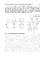
Deshpande et al (1999) achieved white light emission by the sequential energy transfer
between different layers. The device was fabricated in the configuration ITO/
-NPD/-
NPD:DCM2(0.6–8 wt%)/BCP/Alq3/Mg:Ag (20:1)/Ag. Here 4,4’ bis (N-(1-napthyl-N-phenyl-
amino)) biphenyl (α-NPD) was used as a hole injection layer,
-NPD: DCM2 (2, 4-
(dicyanomethylene)-2-methyl-6-(2- (2, 3, 6, 7-tetrahydro-1H, 5H benzo(I, j)quinolizin-8-
yl)vinyl)- 4H-pyran) layer was used as a hole transport layer (HTL) as well as an emitting
layer, 2,9-dimethyl-4,7-diphenyl-1,10- phenanthroline (BCP) layer was deposited for the
purpose of hole blocking, Alq
3
was used as a green emitting electron transporting layer
(ETL) and Mg:Ag alloy followed by a thick layer of Ag was deposited as the cathode.
Organic Light Emitting Diode192
Fig. 7. Schematic diagram of multilayer white OLED
A maximum luminance of 13 500 cd/m
2
, a maximum external quantum efficiency>0.5% and
an average power efficiency of 0.3 lm/W were reported for the above configuration.
Recently Wu et al (2005) reported white light emission from a dual emitting layer OLED
with and without blocking layers. The device with a blocking layer exhibited better
performance with an external quantum efficiency of 3.86%. The emission colour of these
devices strongly depends upon the thickness of the emissive layer and the applied voltage.
The drawback of this technique is that it requires complex processing and a large amount of
wasted organic materials resulting in relatively high fabrication cost. The CIE coordinates
are often dependent upon the driving current due to shift of the exciton recombination zone.
Brian et al (2002) have demonstrated that multi-emissive layer fully electrophosphorescent
WOLEDs can take advantage of the diffusion of triplets to produce bright white devices
with high power and quantum efficiencies. The device color can be tuned by varying the
thickness and the dopant concentrations in each layer, and by introducing exciton blocking
layers between emissive layers.
Gong et al (2005) have reported that high performance multilayer white light emitting
PLEDs can be fabricated by using a blend of luminescent semiconducting polymers and
organometallic complexes as the emission layer and water soluble (or ethanol soluable)PVK-
SO
3
Li as the hole injection/transport layer (HIL/HTL) and t-Bu-PBD-SO
3
Na as the electron
injection/electron transport layer (EIL/ETL). Each layer is spin-cost sequentially from
solution. Illumination quality white light is emitted with stable CIE coordinates, stable
colour temperature and stable clour rendering indices.
Tayagi et al (2010) have demonstrated a WOLED by double layers of blue Zn(hpb)
2
and
yellow Zn(hpb)mq emitting materials. Broad electroluminescence spectrum has been
observed and as the thickness of Zn(hpb)mq layer increases the dominant wavelength shifts
from bluish region to yellowish region. Three peaks have been observed in the EL spectrum
at wavelengths 450 nm, 485 nm and 550 nm. The peak at 450 nm and 485 nm are due to the
recombination of electrons and holes in Zn(hpb)
2
layer and the peak at 550 nm is due to the
recombination in Zn(hpb)mq layer. The peak at 485 nm has been attributed to the excimer
formation in Zn(hpb)
2
. The EL spectrum of duoble layer was found to be an overlap of the
EL spectrum of Zn(hpb)
2
and Zn(hpb)mq layers. CIE coordinates (0.29, 0.38) were well
within the white region and have low turn on voltage (5V).The highest brightness obtained
was 8390 Cd/m
2
at a current density of 518 mA/cm
2
.
White OLEDs which comprised of separate emitters having independent electrodes stacked
one over the other in which separate voltage source control the emission from each device is
known as stacked OLED. Stacking is advantageous due to better luminous efficiency, better
color contrast and good color rendering over a wide range. Furthermore, this tuning
strategy can delay the onset of differential aging of the several emitting layer. It has been
shown that by layering several devices in this manner, a high total brightness OLED can be
achieved without driving any particular element in the stack at such a high intensity that its
operational life time is reduced (Lu and Sturn 2002, Brian et al 2002).
V
Al Al Al
Red emitter Green emitter
Blue emitter
White Light
Glass substrate
ITO
LiF
V
Al Al Al
Red emitter Green emitter
Blue emitter
White Light
Glass substrate
ITO
LiF
(a)
(b)
Fig. 8. Schematic diagram of (a) horizontally and (b) vertically stacked OLED.
Organic Light Emitting Diode for White Light Emission 193
Fig. 7. Schematic diagram of multilayer white OLED
A maximum luminance of 13 500 cd/m
2
, a maximum external quantum efficiency>0.5% and
an average power efficiency of 0.3 lm/W were reported for the above configuration.
Recently Wu et al (2005) reported white light emission from a dual emitting layer OLED
with and without blocking layers. The device with a blocking layer exhibited better
performance with an external quantum efficiency of 3.86%. The emission colour of these
devices strongly depends upon the thickness of the emissive layer and the applied voltage.
The drawback of this technique is that it requires complex processing and a large amount of
wasted organic materials resulting in relatively high fabrication cost. The CIE coordinates
are often dependent upon the driving current due to shift of the exciton recombination zone.
Brian et al (2002) have demonstrated that multi-emissive layer fully electrophosphorescent
WOLEDs can take advantage of the diffusion of triplets to produce bright white devices
with high power and quantum efficiencies. The device color can be tuned by varying the
thickness and the dopant concentrations in each layer, and by introducing exciton blocking
layers between emissive layers.
Gong et al (2005) have reported that high performance multilayer white light emitting
PLEDs can be fabricated by using a blend of luminescent semiconducting polymers and
organometallic complexes as the emission layer and water soluble (or ethanol soluable)PVK-
SO
3
Li as the hole injection/transport layer (HIL/HTL) and t-Bu-PBD-SO
3
Na as the electron
injection/electron transport layer (EIL/ETL). Each layer is spin-cost sequentially from
solution. Illumination quality white light is emitted with stable CIE coordinates, stable
colour temperature and stable clour rendering indices.
Tayagi et al (2010) have demonstrated a WOLED by double layers of blue Zn(hpb)
2
and
yellow Zn(hpb)mq emitting materials. Broad electroluminescence spectrum has been
observed and as the thickness of Zn(hpb)mq layer increases the dominant wavelength shifts
from bluish region to yellowish region. Three peaks have been observed in the EL spectrum
at wavelengths 450 nm, 485 nm and 550 nm. The peak at 450 nm and 485 nm are due to the
recombination of electrons and holes in Zn(hpb)
2
layer and the peak at 550 nm is due to the
recombination in Zn(hpb)mq layer. The peak at 485 nm has been attributed to the excimer
formation in Zn(hpb)
2
. The EL spectrum of duoble layer was found to be an overlap of the
EL spectrum of Zn(hpb)
2
and Zn(hpb)mq layers. CIE coordinates (0.29, 0.38) were well
within the white region and have low turn on voltage (5V).The highest brightness obtained
was 8390 Cd/m
2
at a current density of 518 mA/cm
2
.
White OLEDs which comprised of separate emitters having independent electrodes stacked
one over the other in which separate voltage source control the emission from each device is
known as stacked OLED. Stacking is advantageous due to better luminous efficiency, better
color contrast and good color rendering over a wide range. Furthermore, this tuning
strategy can delay the onset of differential aging of the several emitting layer. It has been
shown that by layering several devices in this manner, a high total brightness OLED can be
achieved without driving any particular element in the stack at such a high intensity that its
operational life time is reduced (Lu and Sturn 2002, Brian et al 2002).
V
Al Al Al
Red emitter Green emitter
Blue emitter
White Light
Glass substrate
ITO
LiF
V
Al Al Al
Red emitter Green emitter
Blue emitter
White Light
Glass substrate
ITO
LiF
(a)
(b)
Fig. 8. Schematic diagram of (a) horizontally and (b) vertically stacked OLED.
Organic Light Emitting Diode194
In a similar concept to the stacked OLED, tunable emitters of different colours (red-, green-,
and blue) are placed side by side in strips. If spaced sufficiently very closely the colors will
merge, as in full color display, producing bright and efficient white light similar to SOLED
emitter with less complexity (Brian et al 2002). This technology is similar to liquid crystal at
panel displays. Here the pixels of the three principal colours are patterned separately either
horizontally or vertically and addressing them independently (Burrows et al 1997, Forrest et
al 1997, Burrows et al 1998) (see Fig. 8). In the horizontally stacked pattern the individual
colour emitting pixels are deposited either in the form of dots, squares, circles, thin lines or
very thin strips. As a result of mixing of these colours any desired range of colours can be
produced in the same pane. As each colour component is addressed individually, the
differential colour ageing can be mitigated by changing the current through the
components. Each pixel can be optimized to operate at a minimum operating voltage and
for highest efficiency. Also by reducing the size of the pixels the lifetime of the device can be
controlled to the maximum.
Stacked white OLEDs usually produce higher brightness and efficiency than those of
conventional WOLED and can be a good candidate as a light source because double or even
triple current efficiency can be obtained in such devices as compared to the single emitter
device. Recently Sun et al (2005) reported an efficient stacked WOLED using a novel anode
cathode layer (ACL) for connecting a blue phosphorescent and red phosphorescent emissive
unit. This ACL layer was used as a middle electrode and EL characteristics of two individual
emissive units were also studied. By biasing the two emissive units in a proper ratio white
emission was obtained. They reported a maximum luminescence of 40000 cd/ m
2
at 26 V
with CIE coordinates of (0.32, 0.38). The luminescence efficiency was 11.6 cd /A at 28 mA/
cm
2
.
Liao et al(2004) and Kido et al (2003) have demonstrated a variant of the SOLED that allows
the contacts between intermediate OLED in the stack to electrically “float” and performs as
a series of independent OLEDs, with a single electron exciting the multiple OLEDs as it
passes through the circuit.
Chang et al (2005) fabricated two types of stacked/tandem WOLEDs containing an
interconnecting layer of Mg:Alq
3
/WO and one control white emitting device for
comparison. In these devices white emission was obtained by mixing complementary blue
and yellow colours. Device 1 was obtained by connecting blue and yellow devices in series,
while device 2 stacked two white emitting devices with the same blue and yellow dopants
as used in device 1. Device 2 shows better performance compared to device1 and the control
device. An interesting amplication effect was observed in device 2 such that it exhibited the
highest efciency of 22 cd /A, which was almost three times that of the control device. This
was due to the microcavity effect, which enhances the amount of light emitted in the
forward direction. This shows that by just connecting two devices higher efficiency can be
achieved. It was found that the driving voltage increases with increasing number of active
units. Device 2 was the least stable, while the control device showed the longest half-life.
This was due to the fact that device 2 suffered more driving power than the control and
device 1. The thermal breakdown process may be present in these stacked devices due to
non-ohmic contact of the interconnecting layers. However the half-life of device 2 at 100 cd/
m
2
was projected to be greater than 80000 h. In these stacked devices the emissive intensity
and colour were dependent on the viewing angle. This viewing angle dependence of
emissive intensity and colour was attributed to the microcavity effect. Therefore it is
important to have a good optical design for the stacked devices. Such device structures had
disadvantages of having complex layer structure and lack of known methods for damage
free post deposition patterning of organic layers at resolution required for color displays.
Another approach for white light emission from multilayer OLEDs is the multiple quantum
well structure (Liu et al 2000) (Fig. 9), which includes two or more emissive layers separated
by blocking layers. Electrons and holes tunnel through the potential barriers of the blocking
layers and distribute uniformly in different wells and emit light. Matching of the energy
levels of different organic materials is not so critical in this system. Excitons are formed in
different wells and decay to produce different coloured lights in their own wells. The
confinement of charge carriers inside the quantum well improves the probability of exciton
formation and they do not move to other zones or transfer their energy to the next zone. But
this approach is very complicated and requires the optimization of thicknesses of various
light emitting and blocking layers. This multilayer architecture has relatively high operating
voltage due to the combined thickness of many layers used.
Fig. 9. Schematic diagram of a multiple quantum well white OLED
4.1.2 Single emissive layer structure
The fabrication process and device operation of white OLEDs through multilayer structure
is very complex and several parameters need to be optimized for good colour rendering and
to have luminescence efficiency. Also, these devices have high operating voltage because of
the thick profile due to the several stacked organic layers used to perform different
functions for efficient WOLEDs. The device profile must be as thin as possible to ensure low
voltage operation. Single layer white light emitting devices consist of only one active
organic layer can emit in the entire visible range and can overcome all such complexities. In
comparison to other structures single layer structure can achieve higher emission colour
stability. White emission from a single layer consisting of a blue emitter doped with
different dyes or blending two or more polymers has been reported by many authors
(Mazzeo et al 2003, Lee et al 2002, Al Attar et al 2005, Tasch et al 1997, Ko et al 2003, Chuen
and Tao 2002, Shao and Yang 2005, Yang et al 2000, Chang et al 2005, Tsai et al 2003).
Organic Light Emitting Diode for White Light Emission 195
In a similar concept to the stacked OLED, tunable emitters of different colours (red-, green-,
and blue) are placed side by side in strips. If spaced sufficiently very closely the colors will
merge, as in full color display, producing bright and efficient white light similar to SOLED
emitter with less complexity (Brian et al 2002). This technology is similar to liquid crystal at
panel displays. Here the pixels of the three principal colours are patterned separately either
horizontally or vertically and addressing them independently (Burrows et al 1997, Forrest et
al 1997, Burrows et al 1998) (see Fig. 8). In the horizontally stacked pattern the individual
colour emitting pixels are deposited either in the form of dots, squares, circles, thin lines or
very thin strips. As a result of mixing of these colours any desired range of colours can be
produced in the same pane. As each colour component is addressed individually, the
differential colour ageing can be mitigated by changing the current through the
components. Each pixel can be optimized to operate at a minimum operating voltage and
for highest efficiency. Also by reducing the size of the pixels the lifetime of the device can be
controlled to the maximum.
Stacked white OLEDs usually produce higher brightness and efficiency than those of
conventional WOLED and can be a good candidate as a light source because double or even
triple current efficiency can be obtained in such devices as compared to the single emitter
device. Recently Sun et al (2005) reported an efficient stacked WOLED using a novel anode
cathode layer (ACL) for connecting a blue phosphorescent and red phosphorescent emissive
unit. This ACL layer was used as a middle electrode and EL characteristics of two individual
emissive units were also studied. By biasing the two emissive units in a proper ratio white
emission was obtained. They reported a maximum luminescence of 40000 cd/ m
2
at 26 V
with CIE coordinates of (0.32, 0.38). The luminescence efficiency was 11.6 cd /A at 28 mA/
cm
2
.
Liao et al(2004) and Kido et al (2003) have demonstrated a variant of the SOLED that allows
the contacts between intermediate OLED in the stack to electrically “float” and performs as
a series of independent OLEDs, with a single electron exciting the multiple OLEDs as it
passes through the circuit.
Chang et al (2005) fabricated two types of stacked/tandem WOLEDs containing an
interconnecting layer of Mg:Alq
3
/WO and one control white emitting device for
comparison. In these devices white emission was obtained by mixing complementary blue
and yellow colours. Device 1 was obtained by connecting blue and yellow devices in series,
while device 2 stacked two white emitting devices with the same blue and yellow dopants
as used in device 1. Device 2 shows better performance compared to device1 and the control
device. An interesting amplication effect was observed in device 2 such that it exhibited the
highest efciency of 22 cd /A, which was almost three times that of the control device. This
was due to the microcavity effect, which enhances the amount of light emitted in the
forward direction. This shows that by just connecting two devices higher efficiency can be
achieved. It was found that the driving voltage increases with increasing number of active
units. Device 2 was the least stable, while the control device showed the longest half-life.
This was due to the fact that device 2 suffered more driving power than the control and
device 1. The thermal breakdown process may be present in these stacked devices due to
non-ohmic contact of the interconnecting layers. However the half-life of device 2 at 100 cd/
m
2
was projected to be greater than 80000 h. In these stacked devices the emissive intensity
and colour were dependent on the viewing angle. This viewing angle dependence of
emissive intensity and colour was attributed to the microcavity effect. Therefore it is
important to have a good optical design for the stacked devices. Such device structures had
disadvantages of having complex layer structure and lack of known methods for damage
free post deposition patterning of organic layers at resolution required for color displays.
Another approach for white light emission from multilayer OLEDs is the multiple quantum
well structure (Liu et al 2000) (Fig. 9), which includes two or more emissive layers separated
by blocking layers. Electrons and holes tunnel through the potential barriers of the blocking
layers and distribute uniformly in different wells and emit light. Matching of the energy
levels of different organic materials is not so critical in this system. Excitons are formed in
different wells and decay to produce different coloured lights in their own wells. The
confinement of charge carriers inside the quantum well improves the probability of exciton
formation and they do not move to other zones or transfer their energy to the next zone. But
this approach is very complicated and requires the optimization of thicknesses of various
light emitting and blocking layers. This multilayer architecture has relatively high operating
voltage due to the combined thickness of many layers used.
Fig. 9. Schematic diagram of a multiple quantum well white OLED
4.1.2 Single emissive layer structure
The fabrication process and device operation of white OLEDs through multilayer structure
is very complex and several parameters need to be optimized for good colour rendering and
to have luminescence efficiency. Also, these devices have high operating voltage because of
the thick profile due to the several stacked organic layers used to perform different
functions for efficient WOLEDs. The device profile must be as thin as possible to ensure low
voltage operation. Single layer white light emitting devices consist of only one active
organic layer can emit in the entire visible range and can overcome all such complexities. In
comparison to other structures single layer structure can achieve higher emission colour
stability. White emission from a single layer consisting of a blue emitter doped with
different dyes or blending two or more polymers has been reported by many authors
(Mazzeo et al 2003, Lee et al 2002, Al Attar et al 2005, Tasch et al 1997, Ko et al 2003, Chuen
and Tao 2002, Shao and Yang 2005, Yang et al 2000, Chang et al 2005, Tsai et al 2003).
Organic Light Emitting Diode196
4.1.2.1 Host Guest structure
One of the most widely used methods to generate white light is host- guest structure. In this
structure often a higher energy-emitting host (donor) material is doped with lower energy
emitting guest (dye, dopant or acceptor) materials to cause energy transfer from the host to
the guests. The dopant site can be excited directly by capturing the charge carriers or by
energy transfer from the host to guest, as a result light emission can come from both the host
and guests, the combined effect of which produces white light and is called emission due to
the incomplete energy transfer. There are many examples where blue and red/orange color
emitting dyes are co-deposited to form the emission layer (Chuen and Tao 2002, Koo et al
2003, Zheng et al 2003, Jiang et al 2002).
An important aspect of host–guest systems is the choice of host and guest materials for both
single and multidoped systems. The energy transfer from host to guest can be either Förster
(Lakowicz 1999) type energy transfer or Dexter type (Turro 1991) charge transfer or due to
the formation of excimer or exciplexes (the principles are discussed in section 5). The
primary conditions for such energy transfers are overlap of the emission spectrum of the
host and absorption spectrum of the guest (Fig. 10). Therefore, the host material is always
one with emission at higher energies, generally a blue-emitting material.
Fig. 10. Spectral overlapping between emission of donor and absorption of acceptor.
The host–guest system for white light generation can be either a single-doped or a multi-
doped system in a single layer (D’Andrade et al 2004) or a multilayer structure (Lim et al
2002). The simplest device structure with a single emitting layer is obtained by doping
primary (Kido et al 1994, Hu and Karasz 2003,) or complementary (Kawamura 2002, Zhang
et al 2003, 2003a) color emitting dyes in a conductive polymer/small molecule host. In these
devices, the concentration of the dopants was so maintained that emission from the host was
small or negligible.
It is not necessary to use only dyes to take advantage of the energy transfer; blends of two
polymers can also be used as host–guest systems (Lee et al 2002). The guest molecules can
be florescent or phosphorescent in nature. However, phosphorescent dyes based on Ir and
Pt complexes have provided significantly higher efficiency of OLEDs because of their ability
to emit from both singlet and triplet excitons of the host molecule (Kamata et al 2002),
whereas a florescent dye can only utilize the singlet exciton. The devices based on
phosphorescent dyes are named as electrophosphorescent devices. Representative examples
of various host materials, florescent and phosphorescent dyes are listed in Table 2.
Host materials 1. Poly(N-vinylcarbazole) (PVK)
2. 1,1,4,4-Tetraphenyl-1,3-butadiene (TPD)
3. 4,4’,N,N’-Dicarbazole-biphenyl (CBP)
4. 9,10-Bis(3’5’-diaryl)phenyl anthracene (JBEM)
5. 9,10-Bis(2’-naphthyl)anthracene (BNA)
6. Bis(2-methyl-8-quinolato) (triphenylsiloxy) aluminum (III)
(SAlq)
7. 4-{4-(N-(1-Naphthyl)-N-phenylaminophenyl)}-1,7-diphenyl-
3,5-dimethyl-1,7-dihydro-dipyrazolo(3,4-b;4’3’-e)pyridine
(PAP-NPA)
8. Bis (2-(2-hydroxyphenyl)benzothiazolate)zinc (Zn(BTZ)
2
)
9. 4,4’Bis(N-(1-naphthyl)-N-phenyl-amino)-biphenyl (-NPD)
Florescent dyes Red 1. 4-(Dicyanomethylene)-2-methyl-6-(p-dimethyl-aminostyryl)-
4H-pyran (DCM1)
2. 4-(Dicyanomethylene)-2-methyl-6-(2-(2,3,6,7-tetrahydro-1H,
5H-benzo(I,j)quinolizin-8-yl)vinyl)-4H-pyran (DCM2) (–)
3.4-(Dicyanomethylene)-2,6-di-(4-dimethylaminobenzaldehyde)-
-pyran (DCDM)
4.4-(Dicyanomethylene)-2-tert-butyl-6(1,1,7,tetramethyljulolidyl-
9-enyl)-4H-pyran (DCJTB)
5. 5,6,11,12-Tetraphenyl-naphthacene (Rubrene) (orange)
6. Zinc tetraphenylporphyrin (ZnTPP)
Green 1. Coumarin6
2. 9-Cyanoanthracene (CNA)
3. Tris(8-quinolato)aluminum (III) (AlQ
3
)
Blue 1. (perylene)
2. 4,4’-Bis(2,2’-diphenylvinyl)-1,1’-biphenyl(DPVBi)
3. 9,10-Bis(3’5’-diaryl)phenyl anthracene(JBEM)
Phosphorescent dyes Red 1. Fac-tris(2-phenyl)-bis(2-(2’-benzothienyl)-pyridinato-
N,C’)(acetylacetonate)Ir(III) (Bt
2
Ir (acac))
2.Bis(2-(2’-benzothienyl)-pyridinato-
N,C
3’
)(acetylacetonate)Ir(III)(Btp
2
Ir (acac))
3.Bis(2-phenylbenzothiozolato-
N,C
2’
)(acetylacetonate)Ir(III)(Bt
2
Ir (acac))
Green Fac-tris(2-phenylpyridyl)iridium(III)(Ir(ppy)
3
)
Blue1.Bis((4,6-difluorophenyl)-pyridinato-
N,C)(picolinato)Ir(III)(FIrpic)
2.Bis{2-(3,5-bis(trifluoromethyl)phenyl)-pyridinato-
N,C
3’
}iridium(III)picolinate ((CF
3
ppy)
2
Ir(pic)) (greenish-
blue)
Table 2. List of various host materials and fluorescent and phosphorescent dyes used for
fabrication of WOLED
Organic Light Emitting Diode for White Light Emission 197
4.1.2.1 Host Guest structure
One of the most widely used methods to generate white light is host- guest structure. In this
structure often a higher energy-emitting host (donor) material is doped with lower energy
emitting guest (dye, dopant or acceptor) materials to cause energy transfer from the host to
the guests. The dopant site can be excited directly by capturing the charge carriers or by
energy transfer from the host to guest, as a result light emission can come from both the host
and guests, the combined effect of which produces white light and is called emission due to
the incomplete energy transfer. There are many examples where blue and red/orange color
emitting dyes are co-deposited to form the emission layer (Chuen and Tao 2002, Koo et al
2003, Zheng et al 2003, Jiang et al 2002).
An important aspect of host–guest systems is the choice of host and guest materials for both
single and multidoped systems. The energy transfer from host to guest can be either Förster
(Lakowicz 1999) type energy transfer or Dexter type (Turro 1991) charge transfer or due to
the formation of excimer or exciplexes (the principles are discussed in section 5). The
primary conditions for such energy transfers are overlap of the emission spectrum of the
host and absorption spectrum of the guest (Fig. 10). Therefore, the host material is always
one with emission at higher energies, generally a blue-emitting material.
Fig. 10. Spectral overlapping between emission of donor and absorption of acceptor.
The host–guest system for white light generation can be either a single-doped or a multi-
doped system in a single layer (D’Andrade et al 2004) or a multilayer structure (Lim et al
2002). The simplest device structure with a single emitting layer is obtained by doping
primary (Kido et al 1994, Hu and Karasz 2003,) or complementary (Kawamura 2002, Zhang
et al 2003, 2003a) color emitting dyes in a conductive polymer/small molecule host. In these
devices, the concentration of the dopants was so maintained that emission from the host was
small or negligible.
It is not necessary to use only dyes to take advantage of the energy transfer; blends of two
polymers can also be used as host–guest systems (Lee et al 2002). The guest molecules can
be florescent or phosphorescent in nature. However, phosphorescent dyes based on Ir and
Pt complexes have provided significantly higher efficiency of OLEDs because of their ability
to emit from both singlet and triplet excitons of the host molecule (Kamata et al 2002),
whereas a florescent dye can only utilize the singlet exciton. The devices based on
phosphorescent dyes are named as electrophosphorescent devices. Representative examples
of various host materials, florescent and phosphorescent dyes are listed in Table 2.
Host materials 1. Poly(N-vinylcarbazole) (PVK)
2. 1,1,4,4-Tetraphenyl-1,3-butadiene (TPD)
3. 4,4’,N,N’-Dicarbazole-biphenyl (CBP)
4. 9,10-Bis(3’5’-diaryl)phenyl anthracene (JBEM)
5. 9,10-Bis(2’-naphthyl)anthracene (BNA)
6. Bis(2-methyl-8-quinolato) (triphenylsiloxy) aluminum (III)
(SAlq)
7. 4-{4-(N-(1-Naphthyl)-N-phenylaminophenyl)}-1,7-diphenyl-
3,5-dimethyl-1,7-dihydro-dipyrazolo(3,4-b;4’3’-e)pyridine
(PAP-NPA)
8. Bis (2-(2-hydroxyphenyl)benzothiazolate)zinc (Zn(BTZ)
2
)
9. 4,4’Bis(N-(1-naphthyl)-N-phenyl-amino)-biphenyl (-NPD)
Florescent dyes Red 1. 4-(Dicyanomethylene)-2-methyl-6-(p-dimethyl-aminostyryl)-
4H-pyran (DCM1)
2. 4-(Dicyanomethylene)-2-methyl-6-(2-(2,3,6,7-tetrahydro-1H,
5H-benzo(I,j)quinolizin-8-yl)vinyl)-4H-pyran (DCM2) (–)
3.4-(Dicyanomethylene)-2,6-di-(4-dimethylaminobenzaldehyde)-
-pyran (DCDM)
4.4-(Dicyanomethylene)-2-tert-butyl-6(1,1,7,tetramethyljulolidyl-
9-enyl)-4H-pyran (DCJTB)
5. 5,6,11,12-Tetraphenyl-naphthacene (Rubrene) (orange)
6. Zinc tetraphenylporphyrin (ZnTPP)
Green 1. Coumarin6
2. 9-Cyanoanthracene (CNA)
3. Tris(8-quinolato)aluminum (III) (AlQ
3
)
Blue 1. (perylene)
2. 4,4’-Bis(2,2’-diphenylvinyl)-1,1’-biphenyl(DPVBi)
3. 9,10-Bis(3’5’-diaryl)phenyl anthracene(JBEM)
Phosphorescent dyes Red 1. Fac-tris(2-phenyl)-bis(2-(2’-benzothienyl)-pyridinato-
N,C’)(acetylacetonate)Ir(III) (Bt
2
Ir (acac))
2.Bis(2-(2’-benzothienyl)-pyridinato-
N,C
3’
)(acetylacetonate)Ir(III)(Btp
2
Ir (acac))
3.Bis(2-phenylbenzothiozolato-
N,C
2’
)(acetylacetonate)Ir(III)(Bt
2
Ir (acac))
Green Fac-tris(2-phenylpyridyl)iridium(III)(Ir(ppy)
3
)
Blue1.Bis((4,6-difluorophenyl)-pyridinato-
N,C)(picolinato)Ir(III)(FIrpic)
2.Bis{2-(3,5-bis(trifluoromethyl)phenyl)-pyridinato-
N,C
3’
}iridium(III)picolinate ((CF
3
ppy)
2
Ir(pic)) (greenish-
blue)
Table 2. List of various host materials and fluorescent and phosphorescent dyes used for
fabrication of WOLED
Organic Light Emitting Diode198
In most of the electrophosphorescence based OLEDs the device quantum efficiencies drop
rapidly with increasing current density and consequently with the brightness due to triplet–
triplet annihilation at high current densities. WOLED based on phosphorescent material had
a maximum forward viewing power efficiency of 26 ± 3 lm W
−1
at low luminosity,
decreasing to 11 ± 1 lm W−1 at 1000 cd m
−2
(Kamata et al 2002, D’Andrade et al 2004).
The color tenability and spectral characteristics in host–guest systems is achieved by
changing the concentration of the dopants and the energy transfer rate to each dopant and
energy transfer between the dopants in multi-doped systems respectively (Kido et al 1994,
Kamata et al 2002, Kawamura et al 2002). The range in which the dopant concentration can
be varied is limited, usually less than 1 wt.% and 10 wt.% for florescent and phosphorescent
dyes, respectively and the upper limit for dopant concentration is due to aggregate
formation at higher concentration or quenching of luminescence due to non-radiative
processes. For example, in a single dopant system, energy transfer from host to guest can be
fast enough to saturate all the guest sites leading to change in spectral characteristics for
higher current densities in a device or higher excitation intensity in PL measurements
(Cheun and Tao 2002, Zheng et al 2003). Similarly, in case of multi-doped systems the
emission from the higher energy dopant increases due to the filled lower energy states
(Kamata et al 2002). Therefore, the concentration ratio of the dopants has to be carefully
balanced in order to have stable white emission over the entire operating conditions of the
device.
Theoretically, for single layer white OLEDs, the organic material should have chromophores
that emit in different visible regions but most of the single molecule used as emitting
material show the photoluminescence (PL) peak in the high-energy blue region (Tsai et al
2003, Paik et al 2002). It is their electroluminescence (EL) that is white or near white, which
implies that some other emitting species like aggregates (Tsai et al 2003) or intramolecular
charge transfer complex (Paik et al 2002) form in the solid state of the film during operation
of the device, which is responsible for the additional peaks in the longer wavelength
regions. Also, the formation of red-shifted peaks and their relative intensity is highly
dependent on the applied bias and thus the emission spectrum is again voltage dependent
(Tsai et al 2003, Paik et al 2002). In the case of emission through aggregates, the relative
intensity of the peaks becomes further dependent on the solvent used for spin coating and
the morphology of the film (Tsai et al 2003). Various molecules that are reported to give
white or near-white emission are listed in Table 3.
Materials Reference
Anthracene fused norbornadiene derivatives (Tsai et al 2003)
Silicon-based alternating copolymers (Paik et al 2002)
containing carbazole and oxadiazole moieties
1,4-Bis-(9-anthrylvinyl)-benzene polymer (Romdhane et al 2003)
Table 3. List of organic molecules that are reported to give white or near-white
electroluminescence
Rai et al (2009) reported the fabrication of a WOLED by using Zn(hpb)
2
doped with an
orange fluorescent dye DCM in the configuration ITO/-NPD/
Zn(hpb)
2
:DCM/BCP/Alq
3
/LiF/Al and obtained white light emission with broad spectrum
for very low concentration of the dye (0.01%). Since Förster type energy transfer (Rai et al
2008a, Shoustikov et al 1998) was improbable at such low dye concentration, the reason for
emission from such low concentration was ascribed as due to trapping of carrier on to dye
molecule followed by recombination. The white EL spectrum (Fig11) of device with suitable
color coordinates was independent of the applied voltage.
Fig. 11. Electroluminescence spectrum of WOLED at 6–10 V.
The most important benefit of OLEDs with only one emission zone over the others is the fact
that high emission colour stability can be achieved. But the approach of white emission by
two or three different light emitting dopants in a single layer has its own problem that
different rates of energy transfer between dopants may lead to colour imbalance. Some
fraction of the highest energy (blue) will readily transfer energy to the green and red
emitters and the green emitter can transfer energy to the red emitter. If the three emitters are
at equal concentrations the red emitter will dominate the spectrum. So the doping ratio must
be blue > green > red at a very carefully balanced ratio.
Shao et al (2005) demonstrated the achievement of highly colour stable WOLED using a
single emissive layer containing a uniformly doped host. To avoid the difficulties in the
precise control of dopants by thermal co-evaporation, the host α-naphthylphenylbiphenyl
diamine (
-NPD) was uniformly doped by the fused organic solid solution method prior to
the deposition with 4,4’-bis(2,2-diphenylethen-1-yl) biphenyl (DPVBi) for the blue emission,
and 10-(2- benzothiazolyl)-2,3,6,7-tetrahydro-1,1,7,7,-tetra methyl-1H, 5H,11H
benzopyrano(6,7,8-ij) quinolizin-11-one (C545T) for the green emission, 5,6,11,12
tetraphenylnaphthacene (rubrene) for the yellow emission and 4-(dicyanomethylene)- 2-
tertbutyl-6-(1,1,7,7 -teramethyljulolidyl -9 –enyl)-4H-pyan (DCJTB) for the red emission. The
correct weight ratio of -NPD, DPVBi, rubrene, DCJTB and C545T for stable white light
emission was 100:5.81:0.342:0.304:0.394. The excitons generated from the blue dopant easily
transfered their energy to other dopants. But the energy transfer from host to guest exhibits
Organic Light Emitting Diode for White Light Emission 199
In most of the electrophosphorescence based OLEDs the device quantum efficiencies drop
rapidly with increasing current density and consequently with the brightness due to triplet–
triplet annihilation at high current densities. WOLED based on phosphorescent material had
a maximum forward viewing power efficiency of 26 ± 3 lm W
−1
at low luminosity,
decreasing to 11 ± 1 lm W−1 at 1000 cd m
−2
(Kamata et al 2002, D’Andrade et al 2004).
The color tenability and spectral characteristics in host–guest systems is achieved by
changing the concentration of the dopants and the energy transfer rate to each dopant and
energy transfer between the dopants in multi-doped systems respectively (Kido et al 1994,
Kamata et al 2002, Kawamura et al 2002). The range in which the dopant concentration can
be varied is limited, usually less than 1 wt.% and 10 wt.% for florescent and phosphorescent
dyes, respectively and the upper limit for dopant concentration is due to aggregate
formation at higher concentration or quenching of luminescence due to non-radiative
processes. For example, in a single dopant system, energy transfer from host to guest can be
fast enough to saturate all the guest sites leading to change in spectral characteristics for
higher current densities in a device or higher excitation intensity in PL measurements
(Cheun and Tao 2002, Zheng et al 2003). Similarly, in case of multi-doped systems the
emission from the higher energy dopant increases due to the filled lower energy states
(Kamata et al 2002). Therefore, the concentration ratio of the dopants has to be carefully
balanced in order to have stable white emission over the entire operating conditions of the
device.
Theoretically, for single layer white OLEDs, the organic material should have chromophores
that emit in different visible regions but most of the single molecule used as emitting
material show the photoluminescence (PL) peak in the high-energy blue region (Tsai et al
2003, Paik et al 2002). It is their electroluminescence (EL) that is white or near white, which
implies that some other emitting species like aggregates (Tsai et al 2003) or intramolecular
charge transfer complex (Paik et al 2002) form in the solid state of the film during operation
of the device, which is responsible for the additional peaks in the longer wavelength
regions. Also, the formation of red-shifted peaks and their relative intensity is highly
dependent on the applied bias and thus the emission spectrum is again voltage dependent
(Tsai et al 2003, Paik et al 2002). In the case of emission through aggregates, the relative
intensity of the peaks becomes further dependent on the solvent used for spin coating and
the morphology of the film (Tsai et al 2003). Various molecules that are reported to give
white or near-white emission are listed in Table 3.
Materials Reference
Anthracene fused norbornadiene derivatives (Tsai et al 2003)
Silicon-based alternating copolymers (Paik et al 2002)
containing carbazole and oxadiazole moieties
1,4-Bis-(9-anthrylvinyl)-benzene polymer (Romdhane et al 2003)
Table 3. List of organic molecules that are reported to give white or near-white
electroluminescence
Rai et al (2009) reported the fabrication of a WOLED by using Zn(hpb)
2
doped with an
orange fluorescent dye DCM in the configuration ITO/-NPD/
Zn(hpb)
2
:DCM/BCP/Alq
3
/LiF/Al and obtained white light emission with broad spectrum
for very low concentration of the dye (0.01%). Since Förster type energy transfer (Rai et al
2008a, Shoustikov et al 1998) was improbable at such low dye concentration, the reason for
emission from such low concentration was ascribed as due to trapping of carrier on to dye
molecule followed by recombination. The white EL spectrum (Fig11) of device with suitable
color coordinates was independent of the applied voltage.
Fig. 11. Electroluminescence spectrum of WOLED at 6–10 V.
The most important benefit of OLEDs with only one emission zone over the others is the fact
that high emission colour stability can be achieved. But the approach of white emission by
two or three different light emitting dopants in a single layer has its own problem that
different rates of energy transfer between dopants may lead to colour imbalance. Some
fraction of the highest energy (blue) will readily transfer energy to the green and red
emitters and the green emitter can transfer energy to the red emitter. If the three emitters are
at equal concentrations the red emitter will dominate the spectrum. So the doping ratio must
be blue > green > red at a very carefully balanced ratio.
Shao et al (2005) demonstrated the achievement of highly colour stable WOLED using a
single emissive layer containing a uniformly doped host. To avoid the difficulties in the
precise control of dopants by thermal co-evaporation, the host α-naphthylphenylbiphenyl
diamine (
-NPD) was uniformly doped by the fused organic solid solution method prior to
the deposition with 4,4’-bis(2,2-diphenylethen-1-yl) biphenyl (DPVBi) for the blue emission,
and 10-(2- benzothiazolyl)-2,3,6,7-tetrahydro-1,1,7,7,-tetra methyl-1H, 5H,11H
benzopyrano(6,7,8-ij) quinolizin-11-one (C545T) for the green emission, 5,6,11,12
tetraphenylnaphthacene (rubrene) for the yellow emission and 4-(dicyanomethylene)- 2-
tertbutyl-6-(1,1,7,7 -teramethyljulolidyl -9 –enyl)-4H-pyan (DCJTB) for the red emission. The
correct weight ratio of -NPD, DPVBi, rubrene, DCJTB and C545T for stable white light
emission was 100:5.81:0.342:0.304:0.394. The excitons generated from the blue dopant easily
transfered their energy to other dopants. But the energy transfer from host to guest exhibits
Organic Light Emitting Diode200
energy losses which has been avoided by the process of direct triplet exciton formation in
the phosphorescent dyes. This leads to reduction in the operating voltage and hence
increases the power efficiency.
D’Andrade et al (2004) reported white light emission from a single emissive layer WOLED.
The emissive layer contained three organometallic phosphorescent dopants: tris(2-
phenylpyridine) iridium(III) (Ir(ppy)
3
) for green light emission, iridium (III)bis(2-
phenylquinolyl-N, C2’) (acetylacetonate) (PQIr) for red light emission and iridium(III)bis(4’,
6’-difluorophenylpyridinato) tetrakis(1-pyrazolyl) borate (FIr6) providing blue light
emission. The materials were simultaneously codoped into wide energy gap p-
bis(triphenylsilyly)benzene (UGH2) host. The triplet doped WOLED exhibited a peak power
efficiency of 42 lm /W with a colour rendering index 80 and a maximum external quantum
efficiency of 12%.
Srivastava et al (2009) used single emission layer device structure in which two
phosphorescent materials were co-doped in suitable ratio and fabricated organic LEDs to get
the white light emission from the devices. The greenish blue and red emission came from
the single emitting layer by an incomplete energy transfer process in which a mixture of
highly efficient phosphorescent materials (FIrPic) (Bis(2-(4,6-difluorophenyl)pyridinato-
N,C
2’
) iridium(III)) (greenish blue) and (Ir-BTPA) (bis(2-(2’-benzothienyl) pyridinato-N,C
3’
)
(acetyl-acetonate) iridium(III)) (red) were used as guest molecules and 4,4’ bis 9 carbozyl
(biphenyl) (CBP) as host. BCP (2, 9 dimethyl 4, 7 diphenyl 1, 1’ phenanthrolene) was used as
hole blocking material. A suitable combination of charge carrier transport material and
electrode materials were used to fabricate white light emitting diodes. Varying dopant
concentrations controls the color of the device (Fig. 12). The maximum luminance of the
device is 4450 cd/m
2
. The CIE coordinates of the device are (0.27, 0.32) which is well within
the white region.
Fig. 12. Electroluminescence spectrum of WOLED at different applied voltages
Further, Rai et al (2010) fabricated an efficient WOLED using a blue light emitting material
namely Zn(hpb)
2
and tuning its spectral response for white light emission by optimally
doping it with bis(2-(2’-benzothienyl) pyridinato-N,C30) iridium(acetylacetonate)
(Ir(btp)
2
acac) that results in emission from both the host and the guest. The blue component
for the white emission has been obtained from the singlet state of the host material Zn(hpb)
2
and red component from the triplet energy transfer from the triplet state of the host to the
triplet state of the guest as shown in Fig. 13. The color coordinates of the white emission
spectrum was controlled by optimizing the concentration of red dopant in the blue
fluorescent emissive layer. Organic light-emitting diodes were fabricated in the
configuration ITO/-NPD/Zn(hpb)
2
:0.01 wt%Ir(btp)
2
acac/BCP/Alq3/LiF/Al. The J–V–L
characteristic of the device shows a turn on voltage of 5 V. The electroluminescence (EL)
spectra of the device cover a wide range of visible region of the electromagnetic spectrum
with three peaks around 450, 485 and 610 nm. A maximum white luminance of 3500 cd/m
2
with CIE coordinates of (x, y=0.34, 0.27) at 15 V has been achieved. The maximum current
efficiency and power efficiency of the device was 5.2 cd/A and 1.43 lm/W respectively at
11.5 V.
EL spectrum of the white emitting device (0.01wt% Ir(btp)
2
acac) at various voltages i.e. 6 to
12V is shown in Fig.14 which consist of emission in red, green and blue of the
electromagnetic spectra.
Fig. 13. Energy transfer mechanism for Zn(hpb)
2
doped with phosphorescent dopant
Ir(btp)
2
acac in electroluminescence process.
Fig. 14 EL spectrum of WOLED at different bias voltage (6 to 12 V).
4.1.2.2 Solution processed WOLED
One of the ways to get white light emission from conjugated polymers is by using blends of
two polymers to extend their emission spectrum (Lee et al 2002, Gong et al 2005, Granstrom
Organic Light Emitting Diode for White Light Emission 201
energy losses which has been avoided by the process of direct triplet exciton formation in
the phosphorescent dyes. This leads to reduction in the operating voltage and hence
increases the power efficiency.
D’Andrade et al (2004) reported white light emission from a single emissive layer WOLED.
The emissive layer contained three organometallic phosphorescent dopants: tris(2-
phenylpyridine) iridium(III) (Ir(ppy)
3
) for green light emission, iridium (III)bis(2-
phenylquinolyl-N, C2’) (acetylacetonate) (PQIr) for red light emission and iridium(III)bis(4’,
6’-difluorophenylpyridinato) tetrakis(1-pyrazolyl) borate (FIr6) providing blue light
emission. The materials were simultaneously codoped into wide energy gap p-
bis(triphenylsilyly)benzene (UGH2) host. The triplet doped WOLED exhibited a peak power
efficiency of 42 lm /W with a colour rendering index 80 and a maximum external quantum
efficiency of 12%.
Srivastava et al (2009) used single emission layer device structure in which two
phosphorescent materials were co-doped in suitable ratio and fabricated organic LEDs to get
the white light emission from the devices. The greenish blue and red emission came from
the single emitting layer by an incomplete energy transfer process in which a mixture of
highly efficient phosphorescent materials (FIrPic) (Bis(2-(4,6-difluorophenyl)pyridinato-
N,C
2’
) iridium(III)) (greenish blue) and (Ir-BTPA) (bis(2-(2’-benzothienyl) pyridinato-N,C
3’
)
(acetyl-acetonate) iridium(III)) (red) were used as guest molecules and 4,4’ bis 9 carbozyl
(biphenyl) (CBP) as host. BCP (2, 9 dimethyl 4, 7 diphenyl 1, 1’ phenanthrolene) was used as
hole blocking material. A suitable combination of charge carrier transport material and
electrode materials were used to fabricate white light emitting diodes. Varying dopant
concentrations controls the color of the device (Fig. 12). The maximum luminance of the
device is 4450 cd/m
2
. The CIE coordinates of the device are (0.27, 0.32) which is well within
the white region.
Fig. 12. Electroluminescence spectrum of WOLED at different applied voltages
Further, Rai et al (2010) fabricated an efficient WOLED using a blue light emitting material
namely Zn(hpb)
2
and tuning its spectral response for white light emission by optimally
doping it with bis(2-(2’-benzothienyl) pyridinato-N,C30) iridium(acetylacetonate)
(Ir(btp)
2
acac) that results in emission from both the host and the guest. The blue component
for the white emission has been obtained from the singlet state of the host material Zn(hpb)
2
and red component from the triplet energy transfer from the triplet state of the host to the
triplet state of the guest as shown in Fig. 13. The color coordinates of the white emission
spectrum was controlled by optimizing the concentration of red dopant in the blue
fluorescent emissive layer. Organic light-emitting diodes were fabricated in the
configuration ITO/-NPD/Zn(hpb)
2
:0.01 wt%Ir(btp)
2
acac/BCP/Alq3/LiF/Al. The J–V–L
characteristic of the device shows a turn on voltage of 5 V. The electroluminescence (EL)
spectra of the device cover a wide range of visible region of the electromagnetic spectrum
with three peaks around 450, 485 and 610 nm. A maximum white luminance of 3500 cd/m
2
with CIE coordinates of (x, y=0.34, 0.27) at 15 V has been achieved. The maximum current
efficiency and power efficiency of the device was 5.2 cd/A and 1.43 lm/W respectively at
11.5 V.
EL spectrum of the white emitting device (0.01wt% Ir(btp)
2
acac) at various voltages i.e. 6 to
12V is shown in Fig.14 which consist of emission in red, green and blue of the
electromagnetic spectra.
Fig. 13. Energy transfer mechanism for Zn(hpb)
2
doped with phosphorescent dopant
Ir(btp)
2
acac in electroluminescence process.
Fig. 14 EL spectrum of WOLED at different bias voltage (6 to 12 V).
4.1.2.2 Solution processed WOLED
One of the ways to get white light emission from conjugated polymers is by using blends of
two polymers to extend their emission spectrum (Lee et al 2002, Gong et al 2005, Granstrom
Organic Light Emitting Diode202
and Inganas 1996). Gong et al (2005) achieved WOLED by using a blend of conjugated
polymers (PFO-ETM and PFO-F (1%)) and organometallic complex (Ir(HFP)
3
) as an emissive
layer. The device exhibited a maximum brightness of 10 000 cd/m
2
at 25 V. The emission of
white light can be understood as the electrons and holes are recombined by two processes:
direct recombination on the main chain (PFO-ETM) to produce blue and green emission in
parallel with electron and hole trapping on the fluorenone units and on the Ir(HFP)
3
followed by radiative recombination with green light from PFO-F (1%) and red light from
the triplet excited states of Ir(HFP)
3
. As a result the mixture of these primary colours gives
white light. The devices had a CCT value of ~4500 K, which is very close to that of sunlight
(~4700 K) at a solar altitude of 22◦ and a CRI value of 86. Both CCT and CRI values were
insensitive to applied voltage and current density. It has been seen that the quality of
emission colour in doped/blend devices is very sensitive to doping/blending concentration
and a minor shift in the dopant or polymer ratio will significantly affect the quality of
colour. This problem can be solved if a single material is used as an emissive layer and the
material has chromophores emitting in the different visible regions. Research is in progress
on the development of white OLEDs based on a single molecule as emissive material (Tsai et
al 2003, Bai et al 2004, Tu et al 2004). Mazzeo et al (2005) reported a bright single layer white
OLED by spin coating a single emitting molecule 3,5 dimethyl 2,6-bis (dimesitylboryl)-
dithieno(3,2’ b:2’,3’-d)thiophene. White emission was achieved by the superposition of
intrinsic blue-green light emission of the single molecule with red shifted emission from
cross-linked dimers. Bright white electroluminescence was obtained with a maximum
luminance of 3800 cd/ m
2
at 18 V and an external quantum efficiency of 0.35%. Tu et al
(2006) reported a successful development of a WOLED by using a single polymer:
polyfluorene derivatives with 1,8-naphthalimide chromophores chemically attached on to
the polyfluorene backbones. Optimization of the relative content of 1,8-naphthalimide
derivatives in the polymer resulted in pure white-light electroluminescence from a single
polymer. The external quantum efficiency of the single emissive WOLEDs is significantly
affected by the thickness of emissive and transport layers. Better device efficiency requires
the optimization of these layers for balanced charge recombination within the emissive
layer.
4.1.3 Exciplex –Excimer structure
OLED characteristics are largely affected by the chemical and physical interaction at
organic/organic interfaces. An interaction of organic materials at interface forms a charge-
transfer excited-state complex which is known as exciplex/excimer (Li et al 2006, Su et al
2007). An exciplex/excimer is a transient charge transfer complex formed due to the
interaction between the excited states of one molecule with the ground state of neighbouring
molecule. The resulting electron–hole pair complex decays radiatively, the emission of
which is considerably red shifted and broadened as compared to the individual molecules.
When the two molecules are same, the transient complex is known as excimer on the other
hand if they are different, they are termed as exciplex. The schematic diagram of the
emission from the exciplex/excimer is shown below (Fig. 15).
Fig. 15. Schematic diagram showing the formation of excimer/exciplex in organic molecule
and light emission from excimer/exciplex molecule is red shifted from the excited monomer
emission.
Depending upon the spin multiplicity, excimer and exciplexes can be fluorescencent or
phosphorescencent. When singlet excited state of the donor molecule interact with the
singlet ground state of acceptor molecule, fluorescence excimer/exciplex are formed where
as interaction of triplet excited state of donor and triplet state of acceptor gives
phosphorescence excimer/exciplex (Fig. 16).
Donor and acceptors, from same molecule excimer are formed
Donor and acceptor, from different molecules exciplex are formed
Fig. 16. Formation of excimer and exciplexes
Organic Light Emitting Diode for White Light Emission 203
and Inganas 1996). Gong et al (2005) achieved WOLED by using a blend of conjugated
polymers (PFO-ETM and PFO-F (1%)) and organometallic complex (Ir(HFP)
3
) as an emissive
layer. The device exhibited a maximum brightness of 10 000 cd/m
2
at 25 V. The emission of
white light can be understood as the electrons and holes are recombined by two processes:
direct recombination on the main chain (PFO-ETM) to produce blue and green emission in
parallel with electron and hole trapping on the fluorenone units and on the Ir(HFP)
3
followed by radiative recombination with green light from PFO-F (1%) and red light from
the triplet excited states of Ir(HFP)
3
. As a result the mixture of these primary colours gives
white light. The devices had a CCT value of ~4500 K, which is very close to that of sunlight
(~4700 K) at a solar altitude of 22◦ and a CRI value of 86. Both CCT and CRI values were
insensitive to applied voltage and current density. It has been seen that the quality of
emission colour in doped/blend devices is very sensitive to doping/blending concentration
and a minor shift in the dopant or polymer ratio will significantly affect the quality of
colour. This problem can be solved if a single material is used as an emissive layer and the
material has chromophores emitting in the different visible regions. Research is in progress
on the development of white OLEDs based on a single molecule as emissive material (Tsai et
al 2003, Bai et al 2004, Tu et al 2004). Mazzeo et al (2005) reported a bright single layer white
OLED by spin coating a single emitting molecule 3,5 dimethyl 2,6-bis (dimesitylboryl)-
dithieno(3,2’ b:2’,3’-d)thiophene. White emission was achieved by the superposition of
intrinsic blue-green light emission of the single molecule with red shifted emission from
cross-linked dimers. Bright white electroluminescence was obtained with a maximum
luminance of 3800 cd/ m
2
at 18 V and an external quantum efficiency of 0.35%. Tu et al
(2006) reported a successful development of a WOLED by using a single polymer:
polyfluorene derivatives with 1,8-naphthalimide chromophores chemically attached on to
the polyfluorene backbones. Optimization of the relative content of 1,8-naphthalimide
derivatives in the polymer resulted in pure white-light electroluminescence from a single
polymer. The external quantum efficiency of the single emissive WOLEDs is significantly
affected by the thickness of emissive and transport layers. Better device efficiency requires
the optimization of these layers for balanced charge recombination within the emissive
layer.
4.1.3 Exciplex –Excimer structure
OLED characteristics are largely affected by the chemical and physical interaction at
organic/organic interfaces. An interaction of organic materials at interface forms a charge-
transfer excited-state complex which is known as exciplex/excimer (Li et al 2006, Su et al
2007). An exciplex/excimer is a transient charge transfer complex formed due to the
interaction between the excited states of one molecule with the ground state of neighbouring
molecule. The resulting electron–hole pair complex decays radiatively, the emission of
which is considerably red shifted and broadened as compared to the individual molecules.
When the two molecules are same, the transient complex is known as excimer on the other
hand if they are different, they are termed as exciplex. The schematic diagram of the
emission from the exciplex/excimer is shown below (Fig. 15).
Fig. 15. Schematic diagram showing the formation of excimer/exciplex in organic molecule
and light emission from excimer/exciplex molecule is red shifted from the excited monomer
emission.
Depending upon the spin multiplicity, excimer and exciplexes can be fluorescencent or
phosphorescencent. When singlet excited state of the donor molecule interact with the
singlet ground state of acceptor molecule, fluorescence excimer/exciplex are formed where
as interaction of triplet excited state of donor and triplet state of acceptor gives
phosphorescence excimer/exciplex (Fig. 16).
Donor and acceptors, from same molecule excimer are formed
Donor and acceptor, from different molecules exciplex are formed
Fig. 16. Formation of excimer and exciplexes
Organic Light Emitting Diode204
In the OLEDs there is a high possibility that exciplex formation occurs at the ETL/EML or
HTL/EML interfaces because HTL and electron transport layer (ETL) usually have an
electron-donating and an electron-accepting nature, respectively. There have been some
researches on the application of exciplexes for the tuning of emission colors (Li et al 2006,
Liang and Choy 2006) and white emitting OLEDs (Tong et al 2007). Extensive studies on
exited bi-molecular complexes and their application in electrophosphorescent devices have
been done by Kalinowski et al (2007) and Cocchi et al (2006).
Mazzeo et al. (2002, 2003, 2003a, Blyth et al 2003) obtained white-light emission by spin
coating the blend of two different blue-emitting molecules having significant spatial overlap
between their LUMOs. The green–red emission from the exciplex combined with the blue
emission from the individual molecules gives white- or near-white-light emission. A host
material can also be doped with two blue emitting and a red emitting material resulting in
green emission from the exciplex, blue and red emission of guests through the energy
transfer from host (Kim et al 2003). The concept of exciplex formation between two blue-
emitting molecules can be extended to multi-layer device design in which these layers are
placed adjacent to each other and the exciplex formation occurs at their interface (Cha and
Jin 2003, Cocchi et al 2002 Liu et al 2002, Fang et al 2004). The exciplex emission is more
favored if the difference between the HOMOs and LUMOs of the two molecules is large.
This will tend to accumulate the charge carriers at the interface, causing increase in the
probability of recombination near the interface. The emission color of these devices is highly
dependent upon the thickness of the layers (Feng et al 2003) and the applied electric field
(Cha and Jin 2003). The layer emitting in the red (Feng et al 2003, 2003a) or green/blue
(Liang et al 2003) region can also be placed adjacent to the cathode if the white light is weak
in intensity for red or green/blue emission.
WOLEDs can also be fabricated based on phosphorescence excimers. A high energy host
organic material is doped with two blue-emitting phosphorescent dyes, namely iridum-
bis(4,6,-difluorophenyl-pyridinato- N, C
2
)-picolinate (FIrpic) and platinum(II)(2-(4’,6’-
difluorophenyl)pyridinato-N, C
2’
)(2,4-pentanedionato) (FPt1) (D’ Andrade et al 2002). The
white emission is obtained by combining the blue monomer emission from FIrpic through
energy transfer from the host and excimer emission from the square planar complex of FPt1.
Another simplification in the device structure is made using a single dopant only and
coupling the monomer and excimer emission of the same molecule (D’ Andrade et al 2002,
Adamovich et al 2002). The monomer to excimer ratio in these devices is very important to
achieve balanced white-light emission and, therefore, the concentration of the dopants
becomes crucial (Adamovich et al 2002, D’ Andrade and Forrest 2003).
Kumar et al (2010) has demonstrated the formation of exciplexes at the -NPD/2-methyl 8-
hydroxy quinolinalo lithium (LiMeq) interface using an ultra thin layer of DCM dye as a
probe. They have placed the thin layer of DCM dye layer (1nm) at different distance from
the interface. The exciplexes formed at the interface transferred their energy to the DCM dye
by a Förster type energy transfer. Excitons were formed at the dye molecule and was
detected which gave its characteristics emission. As the dye layer is moved away from the
interface the intensity of emission from DCM decreased and emission from the exciplex
increased indicating that the exciplexes are generated at the interface only. The maximum
energy transfer was observed when the dye layer was placed at the interface which was
limited by the number of dye molecules. At an optimum distance from the interface the
emission from the exciplexes together with that from the dye gave white light emission. The
origin of exciplex formation was explained as due to a mismatch of the HOMO and LUMO
(Fig17) energies and accumulation of charges at the -NPD/LiMeq interface.
Fig. 17. Energy level diagram showing the formation of exciplexes at the interface
There are several issues involved in formation of exciplexes and excimers that limit the
device performance. In the blended emissive layers, the formation of exciplex strongly
depends on the concentration, structure and morphology of the film (Mazzeo et al 2002). In
such cases fine-tuning of the emission spectrum can be done by concentration variation.
However, there is a limit for concentration variation since phase separation or aggregation
occurs above an optimum concentration, which in turn, will not allow spatial overlap of the
LUMOs of the donor and the acceptor (Mazzeo et al 2002). Another difficulty in exciplex
formation is the temperature dependence since at low temperatures the emission by exciton
recombination will be predominant while at high temperatures, the exciplex emission will
be predominant (Chao and Chen 1998).
The external quantum efficiencies of most of the exiplex emitting devices are usually low
(~1%)(Noda et al 1999, Wang et al 1998, Kawabe and Abe 2002, Cocchi et al 2002). Indeed
the appearance of exiplex is often considered as a major reason for the poor device
performance but the dissociative property of the exiplex of the ground state imparts in to
broad featureless emission band which is red shifted from the parent molecule emission
spectrum. This is the reason that exiplex light emitting devices can be considered as
promising technologies for manufacturing WOLEDs (Feng et al 2001).
4.1.4 Microcavity structure
WOLED fabricated by optical optimization through multimode resonant cavities have also
getting some attention (Singha et al 2003, Dodabalapur 1994, 1994a). The microcavity is a
system consisting of a pair of highly reflecting mirrors having separation of the order of a
micron and utilizes the concept of Fabry-Perot resonant cavity. A resonant microcavity is
formed when the emissive material is sandwiched between two metallic mirrors or a
metallic mirror and semitransparent distributed Bragg reflector (DBR) (Peng et al 2003).
During the operation of device, standing waves are generated, the wavelength of which
depends upon the length and refractive index of the cavity. In conventional structures, light
is wasted since it leaks in all directions. But in a microcavity light emerges only from one
Organic Light Emitting Diode for White Light Emission 205
In the OLEDs there is a high possibility that exciplex formation occurs at the ETL/EML or
HTL/EML interfaces because HTL and electron transport layer (ETL) usually have an
electron-donating and an electron-accepting nature, respectively. There have been some
researches on the application of exciplexes for the tuning of emission colors (Li et al 2006,
Liang and Choy 2006) and white emitting OLEDs (Tong et al 2007). Extensive studies on
exited bi-molecular complexes and their application in electrophosphorescent devices have
been done by Kalinowski et al (2007) and Cocchi et al (2006).
Mazzeo et al. (2002, 2003, 2003a, Blyth et al 2003) obtained white-light emission by spin
coating the blend of two different blue-emitting molecules having significant spatial overlap
between their LUMOs. The green–red emission from the exciplex combined with the blue
emission from the individual molecules gives white- or near-white-light emission. A host
material can also be doped with two blue emitting and a red emitting material resulting in
green emission from the exciplex, blue and red emission of guests through the energy
transfer from host (Kim et al 2003). The concept of exciplex formation between two blue-
emitting molecules can be extended to multi-layer device design in which these layers are
placed adjacent to each other and the exciplex formation occurs at their interface (Cha and
Jin 2003, Cocchi et al 2002 Liu et al 2002, Fang et al 2004). The exciplex emission is more
favored if the difference between the HOMOs and LUMOs of the two molecules is large.
This will tend to accumulate the charge carriers at the interface, causing increase in the
probability of recombination near the interface. The emission color of these devices is highly
dependent upon the thickness of the layers (Feng et al 2003) and the applied electric field
(Cha and Jin 2003). The layer emitting in the red (Feng et al 2003, 2003a) or green/blue
(Liang et al 2003) region can also be placed adjacent to the cathode if the white light is weak
in intensity for red or green/blue emission.
WOLEDs can also be fabricated based on phosphorescence excimers. A high energy host
organic material is doped with two blue-emitting phosphorescent dyes, namely iridum-
bis(4,6,-difluorophenyl-pyridinato- N, C
2
)-picolinate (FIrpic) and platinum(II)(2-(4’,6’-
difluorophenyl)pyridinato-N, C
2’
)(2,4-pentanedionato) (FPt1) (D’ Andrade et al 2002). The
white emission is obtained by combining the blue monomer emission from FIrpic through
energy transfer from the host and excimer emission from the square planar complex of FPt1.
Another simplification in the device structure is made using a single dopant only and
coupling the monomer and excimer emission of the same molecule (D’ Andrade et al 2002,
Adamovich et al 2002). The monomer to excimer ratio in these devices is very important to
achieve balanced white-light emission and, therefore, the concentration of the dopants
becomes crucial (Adamovich et al 2002, D’ Andrade and Forrest 2003).
Kumar et al (2010) has demonstrated the formation of exciplexes at the -NPD/2-methyl 8-
hydroxy quinolinalo lithium (LiMeq) interface using an ultra thin layer of DCM dye as a
probe. They have placed the thin layer of DCM dye layer (1nm) at different distance from
the interface. The exciplexes formed at the interface transferred their energy to the DCM dye
by a Förster type energy transfer. Excitons were formed at the dye molecule and was
detected which gave its characteristics emission. As the dye layer is moved away from the
interface the intensity of emission from DCM decreased and emission from the exciplex
increased indicating that the exciplexes are generated at the interface only. The maximum
energy transfer was observed when the dye layer was placed at the interface which was
limited by the number of dye molecules. At an optimum distance from the interface the
emission from the exciplexes together with that from the dye gave white light emission. The
origin of exciplex formation was explained as due to a mismatch of the HOMO and LUMO
(Fig17) energies and accumulation of charges at the -NPD/LiMeq interface.
Fig. 17. Energy level diagram showing the formation of exciplexes at the interface
There are several issues involved in formation of exciplexes and excimers that limit the
device performance. In the blended emissive layers, the formation of exciplex strongly
depends on the concentration, structure and morphology of the film (Mazzeo et al 2002). In
such cases fine-tuning of the emission spectrum can be done by concentration variation.
However, there is a limit for concentration variation since phase separation or aggregation
occurs above an optimum concentration, which in turn, will not allow spatial overlap of the
LUMOs of the donor and the acceptor (Mazzeo et al 2002). Another difficulty in exciplex
formation is the temperature dependence since at low temperatures the emission by exciton
recombination will be predominant while at high temperatures, the exciplex emission will
be predominant (Chao and Chen 1998).
The external quantum efficiencies of most of the exiplex emitting devices are usually low
(~1%)(Noda et al 1999, Wang et al 1998, Kawabe and Abe 2002, Cocchi et al 2002). Indeed
the appearance of exiplex is often considered as a major reason for the poor device
performance but the dissociative property of the exiplex of the ground state imparts in to
broad featureless emission band which is red shifted from the parent molecule emission
spectrum. This is the reason that exiplex light emitting devices can be considered as
promising technologies for manufacturing WOLEDs (Feng et al 2001).
4.1.4 Microcavity structure
WOLED fabricated by optical optimization through multimode resonant cavities have also
getting some attention (Singha et al 2003, Dodabalapur 1994, 1994a). The microcavity is a
system consisting of a pair of highly reflecting mirrors having separation of the order of a
micron and utilizes the concept of Fabry-Perot resonant cavity. A resonant microcavity is
formed when the emissive material is sandwiched between two metallic mirrors or a
metallic mirror and semitransparent distributed Bragg reflector (DBR) (Peng et al 2003).
During the operation of device, standing waves are generated, the wavelength of which
depends upon the length and refractive index of the cavity. In conventional structures, light
is wasted since it leaks in all directions. But in a microcavity light emerges only from one
Organic Light Emitting Diode206
end of the cavity and the structure is more efficient. By varying the thickness of the layer,
undesirable light can be filtered out and the emission of light can be obtained at any desired
wavelength. Since a microcavity LED is more efficient and uses less current, it lasts longer.
A microcavity resonator is one of the most effective ways of enhancing the luminance and
brightness of monochromatic OLEDs (Hsu et al 2004, Neyts 2005). Spectral narrowing and
intensity enhancement of spontaneous emission in OLEDs by microcavity has been reported
(Juang et al 2005). Dodabalapur et al (1994) demonstrated the control of the emission of
OLEDs by multimode resonant cavities such that the thickness of the cavity is greater than
the single mode cavity devices so that it has several resonant modes within the emission
spectrum of the material. White emission from the microcavity structures is obtained by a
simple modification of the Fabry–Perot resonator (Singha et al 2003) in which combined
emission from the two cavities of different lengths produces white light. Shiga et al (2003)
employed a modified Fabry–Perot resonator cavity with different cavities of different
lengths (see Fig.18, the terms MM, DM, EML and FL represent metallic mirror, dielectric
mirror, emission layer and filter layer, respectively), and produced white light. One
disadvantage of this approach is that the colour coordinates change with viewing angle and
this angular dependence of the emission limits the microcavity applications for white
OLEDs.
Fig. 18. Concept of (a) usual cavity and (b) multiwavelength resonant cavity (MWRC).
4.2 Wavelength conversion
Some blue or ultraviolet light from one OLED is used to excite several phosphors, each of
which emits a different colour and these different colours are mixed to make a white light
with the broadest and richest wavelength spectrum and is called down conversion by
phosphors.
4.2.1 Down conversion by phosphor
A difficulty of colour stability due to differential ageing of various species occurs in several
methods used for white emission from organic LEDs White emission by down conversion
phosphors may be an alternative method in which a blue emitting OLED is coupled with
one or more down conversion phosphor layers. During the operation of the device a small
portion of the blue light is scattered and goes through the phosphors without down
conversion and the phosphor layers absorb emission from the blue OLED and emit
according to their intrinsic property. The mixing of unabsorbed emission from the blue
OLED and the emission from the phosphors produces white light. A schematic diagram of
white light emission by down conversion methode is shown in Fig19. Here only the blue
emitter conducts the charge and is the only site which is directly excited. Once the excitons
are generated they excite other phosphors to produce balanced white emission. As the blue
light emission decreases with age, light from other coupled phosphors should decrease
proportionately because their relative intensities are directly related to those of the blue light
emitter there for there is no differential colour ageing in the down conversion technique.
The emission spectrum can be adjusted by varying the concentration and thickness of the
phosphor layers (Misra et al 2006, Gupta et al 2006).These down conversion WOLEDs
demonstrated the highest CRI value, 93 and efficiency 3.8 lm/W
Fig. 19. Schematic diagram of white light emission by down conversion.
Duggal et al (2002) reported white light emission from a blue OLED coupled with down
converting orange and the red organic phosphor, namely perylene orange and perylene red
dispersed in poly (methacrylate) (PMMA) followed by a layer of inorganic light scattering
phosphor, namely Y(Gd)AG:Ce dispersed in polydimethyl siloxane silicon. The quantum
efficiency of photoluminescence of dyes in PMMA was found to be >98% and the quantum
yield of Y(Gd)AG:Ce was 86%. These down conversion WOLEDs demonstrated the highest
CRI value, 93 and efficiency 3.8 lm/W.
In Materials Research Society meeting 2005 (MRS Fall Meeting, 28 November– 2 December
2005, Boston, MA, USA) one of the biggest changes pioneered by Junji Kido and Forrest’s
groups has been the switching from fluorescent materials to phosphorescent materials.
Phosphorescent dyes can convert both singlet and triplet excitons into light, making the
devices potentially much more efficient. They reported a new blue OLED based on
phosphorescent compound FIrpic, with a record breaking efficiency of 42 lm/ W at 100 cd
m
−2
. They surrounded the FIrpic containing layer with layers of other compounds that allow
triplet excitons to reside within the emissive layer. This creates an energetic well in the light
emitting material so that excitons cannot get out and they decay in the presence of blue
phosphor to give off blue light. To get white light they added a yellow phosphor to their
blue light emitting layer, converting some of the emitted light to yellow, which combined
with the blue to give off white light. The light photons emitted from OLEDs reflect off the
glass–air interface and bounce back inside the device, where many of them are reabsorbed
and generate heat instead of light. The efficiency of OLEDs has been boosted (36 lm/W to 57
lm/W) by adding a specialized antireflective coating to the outside of the glass.
White emission from down conversion can also be obtained by coupling UV light with red,
green and blue phosphors which excites several phosphors, each of which emits a different
colour, as a result of mixing these colours white light emission is obtained. The technique
Organic Light Emitting Diode for White Light Emission 207
end of the cavity and the structure is more efficient. By varying the thickness of the layer,
undesirable light can be filtered out and the emission of light can be obtained at any desired
wavelength. Since a microcavity LED is more efficient and uses less current, it lasts longer.
A microcavity resonator is one of the most effective ways of enhancing the luminance and
brightness of monochromatic OLEDs (Hsu et al 2004, Neyts 2005). Spectral narrowing and
intensity enhancement of spontaneous emission in OLEDs by microcavity has been reported
(Juang et al 2005). Dodabalapur et al (1994) demonstrated the control of the emission of
OLEDs by multimode resonant cavities such that the thickness of the cavity is greater than
the single mode cavity devices so that it has several resonant modes within the emission
spectrum of the material. White emission from the microcavity structures is obtained by a
simple modification of the Fabry–Perot resonator (Singha et al 2003) in which combined
emission from the two cavities of different lengths produces white light. Shiga et al (2003)
employed a modified Fabry–Perot resonator cavity with different cavities of different
lengths (see Fig.18, the terms MM, DM, EML and FL represent metallic mirror, dielectric
mirror, emission layer and filter layer, respectively), and produced white light. One
disadvantage of this approach is that the colour coordinates change with viewing angle and
this angular dependence of the emission limits the microcavity applications for white
OLEDs.
Fig. 18. Concept of (a) usual cavity and (b) multiwavelength resonant cavity (MWRC).
4.2 Wavelength conversion
Some blue or ultraviolet light from one OLED is used to excite several phosphors, each of
which emits a different colour and these different colours are mixed to make a white light
with the broadest and richest wavelength spectrum and is called down conversion by
phosphors.
4.2.1 Down conversion by phosphor
A difficulty of colour stability due to differential ageing of various species occurs in several
methods used for white emission from organic LEDs White emission by down conversion
phosphors may be an alternative method in which a blue emitting OLED is coupled with
one or more down conversion phosphor layers. During the operation of the device a small
portion of the blue light is scattered and goes through the phosphors without down
conversion and the phosphor layers absorb emission from the blue OLED and emit
according to their intrinsic property. The mixing of unabsorbed emission from the blue
OLED and the emission from the phosphors produces white light. A schematic diagram of
white light emission by down conversion methode is shown in Fig19. Here only the blue
emitter conducts the charge and is the only site which is directly excited. Once the excitons
are generated they excite other phosphors to produce balanced white emission. As the blue
light emission decreases with age, light from other coupled phosphors should decrease
proportionately because their relative intensities are directly related to those of the blue light
emitter there for there is no differential colour ageing in the down conversion technique.
The emission spectrum can be adjusted by varying the concentration and thickness of the
phosphor layers (Misra et al 2006, Gupta et al 2006).These down conversion WOLEDs
demonstrated the highest CRI value, 93 and efficiency 3.8 lm/W
Fig. 19. Schematic diagram of white light emission by down conversion.
Duggal et al (2002) reported white light emission from a blue OLED coupled with down
converting orange and the red organic phosphor, namely perylene orange and perylene red
dispersed in poly (methacrylate) (PMMA) followed by a layer of inorganic light scattering
phosphor, namely Y(Gd)AG:Ce dispersed in polydimethyl siloxane silicon. The quantum
efficiency of photoluminescence of dyes in PMMA was found to be >98% and the quantum
yield of Y(Gd)AG:Ce was 86%. These down conversion WOLEDs demonstrated the highest
CRI value, 93 and efficiency 3.8 lm/W.
In Materials Research Society meeting 2005 (MRS Fall Meeting, 28 November– 2 December
2005, Boston, MA, USA) one of the biggest changes pioneered by Junji Kido and Forrest’s
groups has been the switching from fluorescent materials to phosphorescent materials.
Phosphorescent dyes can convert both singlet and triplet excitons into light, making the
devices potentially much more efficient. They reported a new blue OLED based on
phosphorescent compound FIrpic, with a record breaking efficiency of 42 lm/ W at 100 cd
m
−2
. They surrounded the FIrpic containing layer with layers of other compounds that allow
triplet excitons to reside within the emissive layer. This creates an energetic well in the light
emitting material so that excitons cannot get out and they decay in the presence of blue
phosphor to give off blue light. To get white light they added a yellow phosphor to their
blue light emitting layer, converting some of the emitted light to yellow, which combined
with the blue to give off white light. The light photons emitted from OLEDs reflect off the
glass–air interface and bounce back inside the device, where many of them are reabsorbed
and generate heat instead of light. The efficiency of OLEDs has been boosted (36 lm/W to 57
lm/W) by adding a specialized antireflective coating to the outside of the glass.
White emission from down conversion can also be obtained by coupling UV light with red,
green and blue phosphors which excites several phosphors, each of which emits a different
colour, as a result of mixing these colours white light emission is obtained. The technique
Organic Light Emitting Diode208
has colour stability but the losses associated with wavelength conversion are the main
drawbacks of this technique.
There is a lack of theoretical modelling of electroluminescence in OLEDs. Tyagi et al (2010)
has developed a model based on Monte-Carlo simulation technique (Ries et al 1988, Ries
and Bässler1987, Movaghar et al 1986, Houili et al 2006) to model the disordered
semiconductor (assuming Gaussian density of states) to generate the electroluminescence
spectrum of multilayer OLED for white light emission. The electroluminescence (EL)
spectrum in an OLED was generated by the recombination of a positive charge carrier with
a negative charge carrier in the emitting layer. The emitted photons have energy equal to the
difference of energies of negative and positive charge carriers.
5. Photo physics of White OLEDs
Doping of wide band gap materials which emits in the blue region of the spectrum with
lower band gap dopants can modify the emission properties of the host molecules. The
modification of emission properties upon doping is due to efficient energy transfer process
from the host molecules to the guest molecules (dopants) and with careful balancing of the
doping it is possible to obtain white light emission. The dopants can be fluorescent or
phosphorescent in nature. The dopant site can be excited directly or by energy/charge
transfer from the host molecule.
The energy transfer in this matrix occurs in different ways. They are (i) Forster type energy
transfer, (ii) Dexter transfer (iii) Exciplex - excimer charge transfer and (iv)Trap assisted
recombination. The principles are discussed below.
5.1 Förster Type energy transfer
A molecule that is in an excited singlet or triplet state (Donor) can transfer its energy to a
molecule in the ground state (Acceptor) by electronic energy transfer (ET). Energy transfer
always involves two molecules that are in close proximity to each other. It is the
fundamental process of energy / exciton migration which consists of multiple energy
transfer processes. Radiationless energy transfer can occur via a dipole-dipole interaction
having a long range separation of about ~30-100A known as Förster transfer or via
exchange of electrons through overlapping orbitals termed as Dexter transfer. The Forster
energy transfer requires spectral overlap of the emission spectrum of the donor with the
absorption spectrum of the acceptor. The radiation field of the dipole transition of D is
coupled with the dipole transition of A through space without the requirement of spatial
overlap of wavefunctions and can be explained as
D* + A XD+A+h
where D*, A, X, D and h stand for excited donor, ground state of acceptor, intermediate
excited system, ground state of donor and energy of emitted photon respectively. A scheme
of Förster transfer is depicted in Fig. 20. The left side of Fig. 20 shows energy transfer
between molecules of similar singlet energy. This is possible due to the weak overlap of
absorption and emission spectra of identical molecules. The right side shows energy transfer
to a molecule which is lower in its singlet energy (trap state). In both cases the ET occurs
radiationless.
Fig. 20. Simplified scheme of resonant energy Forster energy transfer between a donor (D)
and an acceptor (A). Right side shows energy transfer to a trap which is lower in its singlet
energy.
Furthermore the fluorescence lifetime of the donor molecules is significantly reduced as a
consequence of efficient energy transfer to the lower energy trap. Since Förster energy
transfer is mediated by dipole-dipole interaction without the need of direct overlap of
orbitals, it can overcome distances up to 10 nm. It allows only singlet-singlet transition at
low acceptor concentration and at a much faster rate of <10
-9
s.
5.2 Dexter transfer
The second possibility of energy transfer is known as exchange type or Dexter energy
transfer. Dexter ET is based on quantum mechanical exchange interactions, therefore it
needs strong spatial overlap of the involved wavefunctions of D and A. Since the overlap of
electronic wavefunctions decays exponentially with distance, it is expected that the rate
constant k
DA
decreases even more rapidly with distance R than observed in the case of
singlet transfer. A schematic presentation of Dexter ET is shown in Fig. 21. Dexter ET occurs
typically over distances which are similar to the van-der-Waals distance, i.e. R = 0.5 - 1nm.
The rate constant drops exponentially with the distance R
DA
between D and A: