Advances in Solid State Part 13 pptx
Bạn đang xem bản rút gọn của tài liệu. Xem và tải ngay bản đầy đủ của tài liệu tại đây (2.19 MB, 30 trang )
17
Liquid Phase Oxidation on InGaP
and Its Applications
Yeong-Her Wang
1
and Kuan-Wei Lee
2
1
Institute of Microelectronics, Department of Electrical Engineering,
Advanced Optoelectronic Technology Center, National Cheng-Kung University, Tainan 701,
2
Department of Electronic Engineering, I-Shou University, Kaohsiung County 840,
Taiwan
1. Introduction
High-electron-mobility transistors (HEMTs) and heterojunction bipolar transistors (HBTs)
have attracted many attentions in high speed and power applications due to the superior
transport properties. As compared to AlGaAs pseudomorphic HEMTs (PHEMTs), InGaP-
related devices have advantages, such as higher band gaps, higher valence-band discontinuity
[1], negligible deep-complex (DX) centers [2], excellent etching selectivity between InGaP and
GaAs, good thermal stabilities [3-5], higher Schottky barrier heights [3], and so on. Particularly,
the use of an undoped InGaP insulator takes the advantages of its low DX centers and low
reactivity with oxygen [6-10], which may still suffer from the high gate leakage issue. In order
to inhibit the gate leakage issue, increase the power handling capabilities, and improve the
breakdown voltages, a metal-oxide-semiconductor (MOS) structure has been widely
investigated. However, it is still lacks a reliable native oxide film growing on InGaP, and very
few papers have reported on InGaP/InGaAs MOS-PHEMTs. In addition, the MOS-PHEMT
not only has the advantages of the MOS structure (e.g., lower leakage current and higher
breakdown voltage) but also has the high-density, high-mobility 2DEG channel.
Over the past years, a study on the liquid phase oxidation (LPO) of InGaP near room
temperature has been done [11-14]. The application of surface passivation to improve the
InGaP/GaAs HBTs’ performance has also been first demonstrated [13]. The InGaP/GaAs
HBTs with surface passivation by LPO exhibit significant improvement in current gain at
low collector current regimes due to the reduction of surface recombination current, as
compared to those without surface passivation. Moreover, a larger breakdown voltage and a
lower base recombination current are also obtained. In this chapter, the oxide film
composition and some issues are addressed. Then a thin InGaP native oxide film prepared
by the LPO as the gate dielectric for InGaP/InGaAs MOS-PHEMTs application are
discussed, and the comparisons between devices with and without LPO passivation on the
InGaP/GaAs HBTs are also reviewed.
2. Characterization of the oxide film
The root mean square (rms) value of surface roughness for the In
0.49
Ga
0.51
P sample is
estimated to be 1.1 nm before oxidation (i.e., as received) by AFM measurement, and can be
Advances in Solid State Circuits Technologies
352
improved to 0.95 nm after oxidation (i.e., as grown), as shown in Fig. 1. Fig. 2 shows the
SIMS depth profiles before and after liquid phase oxidation on In
0.49
Ga
0.51
P. Although LPO
on InGaP material has a much slower oxidation rate which is less than 10 nm/h, as
comparing to that of the GaAs material, however, it is still feasible to grow a thin oxide film
without pH control [15, 16]. The oxidation rate becomes significantly saturated when the
oxidation time is longer than an hour, which is measured using a Veeco Instrument
DEKTAK and confirmed by SEM.
The XPS depth profiles of the LPO-grown oxide for In
0.49
Ga
0.51
P are shown in Fig. 3(a). Fig.
3(b)-(d) show the XPS surface spectra of the Ga-3d, In-3d, and P-2p core levels, respectively.
The binding energies for all spectra are calibrated with the reference (as-received) signal.
The as-received sample was dipped into a solution of HF:H
2
O = 1:200 for 30 s before
measurement. From Fig. 3(c)-(d), in comparison with the previous paper [17], the spectrum
is rather similar to that of InPO
4
. This is also confirmed by the values of the O-1s peak
energy and energy separations between the main core levels (i.e., Ga-3d, In-3d, and P-2p) in
the oxide phases [18]. This clearly suggests that the oxide film is mostly composed of InPO
4
-
like and Ga oxide. In addition, the oxide film may appear to be etched back in the growth
solution after 2 h of oxidation. The thermal stability of the oxide layer is also important in
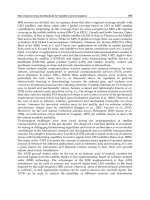
2 h oxidation
rms: 0.95 nm
LPO
rms: 1.1 nm
as received
Fig. 1. AFM images of the In
0.49
Ga
0.51
P sample before (i.e., as received) and after (i.e., as
grown) liquid phase oxidation.
Liquid Phase Oxidation on InGaP and Its Applications
353
0.00 0.02 0.04 0.06 0.08 0.10
10
1
10
2
10
3
10
4
10
5
10
6
P
Depth (
μm)
Secondary ion counts
as received
In
Ga
O
(a)
0.00 0.02 0.04 0.06 0.08 0.10
10
1
10
2
10
3
10
4
10
5
10
6
P
O
In
Ga
as grown
(50
o
C, 1 h oxidation)
Depth (μm)
Secondary ion counts
(b)
Fig. 2. SIMS depth profiles of the In
0.49
Ga
0.51
P sample before (i.e., as received) and after (i.e.,
as grown) liquid phase oxidation.
device fabrications because high-temperature processes are usually required. Again, XPS is
utilized to also important in device fabrications because high-temperature processes are
usually required. Again, XPS is utilized to analyze the surface chemistry of the oxide films,
as shown in Fig. 3. After 2 h of oxidation, the RTA processes were performed in a furnace
Advances in Solid State Circuits Technologies
354
with N
2
flowing at 300-700
o
C for 1 min [13]; however, a peak of InPO
4
-like is still observed.
InPO
4
(bandgap energy = 4.5 eV) is chemically stable and has rather good dielectric
properties [19]. As a result, the InPO
4
probably acts as a capping layer for the entire oxide
film to enhance the thermal stability. However, the experimental results show that high-
temperature treatments (700
o
C) will change the properties of Ga
2
O
3
, since the XPS energy
peak of Ga
2
O
3
shifts to a lower binding energy, and the binding energy is inferred to form
the GaO
x
or Ga
2
O
x
.
(a)
(b)
Liquid Phase Oxidation on InGaP and Its Applications
355
(c)
(d)
Fig. 3. (a) The XPS depth profiles of the as-grown oxide film on In
0.49
Ga
0.51
P.
The (b)-(d) show the XPS surface spectra for the Ga-3d, In-3d, and P-2p core levels,
respectively.
3. InGaP/InGaAs MOS-PHEMT
3.1 Experimental
Figure 4 schematically shows the PHEMT structure grown by the metallorganic chemical
vapor deposition (MOCVD) on a semi-insulating GaAs substrate. Hall measurement
indicates that the electron mobility is 4000 cm
2
/V·s, and the electron sheet density is
2.2×10
12
cm
-2
at room temperature [11]. The device isolation was accomplished by mesa wet
Advances in Solid State Circuits Technologies
356
etching down to the buffer layer. The ohmic contacts of the Au/Ge/Ni metal were
deposited by evaporation and then were patterned by lift-off processes, followed by RTA.
The depth of gate recess is 110 nm for reference PHEMT and 100 nm for MOS-PHEMT.
After etching the capping layer and the partial Schottky layer, an LPO growth solution was
used to generate the gate oxide for the MOS-PHEMT at 50
o
C for 30 min. Finally, the gate
electrode was formed with Au. Moreover, the oxide layer, as illustrated in the figure, also
selectively and simultaneously passivated the isolated surface sidewall. The gate dimension
is 2×100 μm
2
with a drain-to-source spacing of 5 μm.
Source
Drain
Gate
S. I. GaAs Substrate
Oxide Layer
GaAs Buffer Layer
i-In
0.15
Ga
0.85
As Channel Layer 14 nm
AlGaAs Barrier Layer
InGaP Barrier Layer
2DEG
PHEMT MOS-PHEMT
n
+
GaAs
60 nm
DrainSource
n-InGaP
Gate
70 nm
n
+
GaAs
60 nm
DrainSource
n-InGaP
Gate
70 nm
318
102.118
−
×− cmnmInGaPn
n
m
InGaPi 2−
GaAs 60 nm
5 x 10
18
cm
-3
317
0.510.49
cm101nm70PGaInn
−
×−
Fig. 4. The schematic drawing of the InGaP/InGaAs MOS-PHEMT.
3.2 Results and discussion
Figure 5(a) compares the measured I-V characteristics of the MOS-PHEMT with those of the
reference PHEMT fabricated under identical conditions. Clearly, good pinch-off and
saturation current characteristics are obtained. Due to the higher energy barriers between
the metal gate and the Schottky layer, the MOS-PHEMT can be operated at higher gate-to-
source voltage (V
GS
) and drain-to-source voltage (V
DS
) than those of the conventional
Schottky gate PHEMT, which can enhance the current driving capability. Fig. 5(b) compares
the transconductance g
m
and the drain current density I
D
as a function of V
GS
at V
DS
= 4 V of
the MOS-PHEMTs with those of the reference PHEMT. For MOS-PHEMT, the 1.8 V-wide
gate voltage swing (defined by 10% reduction from the maximum g
m
) is higher than that of
the PHEMT. The threshold voltage V
th
of MOS-PHEMT shifts to the left, which is similar to
the result of the one with oxide deposited on the Schottky layer [20, 21]. However, the
separation region between the oxide-InGaP interface and the InGaAs channel for MOS-
Liquid Phase Oxidation on InGaP and Its Applications
357
PHEMT is still larger than that of the reference PHEMT in this study, so the drain current
density of the PHEMT is smaller than that of the MOS-PHEMT at the same bias V
GS
due to
the decrease of the carrier concentration within the InGaAs 2DEG channel.
(a)
(b)
Fig. 5. (a) Measured I-V characteristics of MOS-PHEMT and PHEMT. (b) The
transconductance and the drain current density versus V
GS
at V
DS
= 4 V for the MOS-
PHEMT and the reference PHEMT.
Advances in Solid State Circuits Technologies
358
In addition, if the depth of gate recess is etched to be 120 nm, the V
th
becomes more positive,
-0.5 V, for MOS-PHEMT with the identical processing conditions including initial pH value
(5.0), temperature (50
o
C), and oxidation time (30 min). For V
th
shifts to the right, the
separation between the oxide-InGaP layer interface and the InGaAs channel layer is
decreased due to the consumption of the InGaP during the processes of gate recess and the
unique properties of the LPO with the reaction of InGaP, leading to the increase of the total
effect of the gate bias on the control of V
th
. However, a decrease in the maximum g
m
, 63
mS/mm, accompanies the degradation in the saturation current, 84 mA/mm at V
GS
= 1 V.
The result is also confirmed by a longer oxidation time, i.e., a thicker oxide layer. This
drawback can be overcome by suitable device structures, such as inserting a Si-planar
doping layer under the InGaAs channel to increase the carrier density.
The oxide film provides an improvement in the breakdown voltage in terms of the gate
leakage current of the MOS structure, supported by the typical gate-to-drain I-V
characteristics, as shown in Fig. 6(a). For InGaP MOS-PHEMT, the turn-on voltage, 2.2 V, is
obviously higher than that of InGaP PHEMT, 0.8 V, and the corresponding reverse gate-to-
drain breakdown voltages, BV
GD
, are -14.1 V and -6.5 V, respectively. The turn-on voltage
and the BV
GD
are defined as the voltage at which the gate current reaches 1 mA/mm. The
gate leakage current can be suppressed at least by more than two orders of magnitude with
an oxide film at V
GD
= -4 V. The smaller gate leakage current of MOS-PHEMT is due to the
MOS structure and the elimination of sidewall leakage paths that are directly passivated
during the oxidation, which is consistent with the result of Fig. 5. In addition, the gate
leakage current observed in MOS-PHEMT comes from a gate leakage path at the edge of the
mesa [22] that is not present in the MOS capacitor, which may contribute to the Schottky-
like I-V characteristics for forward biases. Fig. 6(b) shows the gate current density as a
function of reverse V
GS
at different V
DS
. Due to the high electric field existing in the gate-to-
drain region, hot electron phenomena occur in the narrow band-gap InGaAs channel.
Electrons can obtain higher energy to generate electron-hole pairs through the enhanced
impact ionization, resulting in easy injection of the holes into the gate terminal [23].
However, in InGaP-related devices, it is more difficult for the holes generated by the impact
ionization to overcome the valence band discontinuity and to reach the gate [4], so the bell
shaped behavior of the impact ionization does not appear in Fig. 6. Moreover, the gate
current density of MOS-PHEMT is significantly improved, which is less than 0.5 μA/mm, as
compared to that of PHEMT. In other words, the electrons and holes generated by the
impact ionization are decreased to further reduce the drain and gate currents owing to the
oxide layer with a high barrier height.
In order to have a better insight into the transient behavior of the studied devices, the gate
pulse measurements were performed using a Tektronix 370A curve tracer [24]. V
GS
was
pulsed from the V
th
to 0 V with a pulsewidth of 80 μs, while V
DS
was swept from 0 to 4 V.
The comparisons between the static and pulsed I-V characteristics for PHEMT and MOS-
PHEMT are shown in Fig. 7. The drain current of PHEMT decreased by 9.8%, while the
MOS-PHEMT decreased by only 0.63%. To the best of our knowledge, if the pulsewidth is
too short, electrons captured by the traps do not have enough time to be fully emitted.
However, if the pulsewidth is long enough, all the trapped electrons are de-trapped and will
contribute to the drain current. We believe that the differences between dc and pulsed I-V
become evident by applying shorter voltage pulses to the gate such as less than 10-μs pulses
for PHEMT and MOS-PHEMT. Therefore, it is clear that the oxide passivation on the
Liquid Phase Oxidation on InGaP and Its Applications
359
Schottky layer can minimize the effect of surface traps, which is consistent with the lower
gate leakage current in Fig. 6.
-14 -12 -10 -8 -6 -4 -2 0 2
10
-7
10
-6
10
-5
10
-4
10
-3
10
-2
10
-1
10
0
Gate current density (mA/mm)
Gate-to-drain voltage V
GD
(V)
InGaP MOS-PHEMT
InGaP PHEMT
(a)
-2.0 -1.5 -1.0 -0.5 0.0
-180
-160
-140
-120
-100
-80
-60
-40
-20
0
InGaP MOS-PHEMT
V
DS
= 4 V to 7 V,
step = 0.5 V
InGaP PHEMT
V
DS
= 4 V to 5 V,
step = 0.5 V
Gate current density (μA/mm)
Gate-to-source voltage V
GS
(V)
(b)
Fig. 6. (a) The typical I
G
-V
GD
characteristics of PHEMT with and without an oxide film. (b)
The gate current density versus reverse V
GS
at different V
DS
.
Advances in Solid State Circuits Technologies
360
(a)
(b)
Fig. 7. Gate pulse measurements for (a) reference PHEMT and (b) MOS-PHEMT with V
GS
pulsed from V
th
to 0 V with a pulsewidth of 80 μs, while V
DS
was swept from 0 to 4 V.
4. InGaP/GaAs HBT with LPO passivation
4.1 Experimental
The structure used for HBT is given in Table 1. The epilayers were grown by a low-pressure
MOCVD system on an (100)-oriented semi-insulating (S.I.) GaAs substrate. For InGaP/GaAs
HBTs, device fabrication began with emitter definition. The emitter cap layer was removed
and stopped at the InGaP active layer. After removing the InGaP layer, a growth solution
Liquid Phase Oxidation on InGaP and Its Applications
361
was used to form the base oxide (passivation) on the exposed extrinsic surface of base and
the base contact was then deposited. Finally, the mesa of base was defined and etched to
sub-collector before the collector contact deposition. H
3
PO
4
-based etchant was used for
GaAs and InGaP. The Au/Ge and Au/Be metals were deposited by evaporation and
patterned by lift-off processing to form emitter, base and collector regions, respectively.
Layer
Material Thickness (nm) Dopant (cm
-3
)
Cap
Graded
Sub-emitter
Emitter
Base
Collector
Etching-stop
Sub-collector
InGaAs
InGaAs
GaAs
InGaP
GaAs
GaAs
InGaP
GaAs
45
45
130
40
100
750
20
600
1×10
19
1×10
19
5×10
18
3×10
17
4×10
19
1×10
16
5×10
18
5×10
18
S.I. GaAs substrate
Table 1. The epitaxial structure of InGaP/GaAs HBT.
4.2 Results and discussion
Figure 8 shows the common-emitter I-V characteristics of the HBT with and without surface
passivation by LPO. Clearly, the dc current gain (β) of HBTs with passivation is improved
(increased) 15% when comparing to HBTs without passivation. The higher β with surface
passivation is due to the reduction of the surface recombination current in the exposed
extrinsic base regions by LPO method. The common-emitter I-V characteristics of the
devices with and without surface passivation at low collector current regimes are shown
Fig. 8. Common-emitter I-V characteristics of the HBTs with and without LPO passivation.
Advances in Solid State Circuits Technologies
362
in Fig. 9. The devices with surface passivation have higher common-emitter β than those
devices without passivation, due to the reduction of the surface combination velocity by
using an oxide layer on the base surface. In addition, the β values with and without
passivation are 13.3 and 2 at I
B
= 900 pA, respectively. The maximum increase of 7 fold in
the current gain at collector current down to nA level.
0.0 0.5 1.0 1.5 2.0
-2
0
2
4
6
8
10
12
14
16
I
C
(nA)
V
CE
(V)
without passivation
I
B
=100 pA/step
I
B
=900pA
(a)
0.00.51.01.52.0
-2
0
2
4
6
8
10
12
14
16
I
B
=100 pA/step
I
C
(nA)
V
CE
(V)
with LPO passivation
I
B
=900pA
(b)
Fig. 9. Common-emitter I-V characteristics of the HBTs (a) without and (b) with LPO
passivation at low collector current regimes.
Figure 10 illustrates the measured Gummel plots of the devices with and without LPO
passivation. The collector currents are almost identical without being affected by the
passivation treatment. However, a decrease of the base leakage current at low collector
Liquid Phase Oxidation on InGaP and Its Applications
363
current levels is obviously observed after oxidation. Moreover, it is found that the
recombination current at the extrinsic base region and the base-emitter perimeter are
competed against one another, resulting in current reduction at lower base-emitter bias V
BE
= 0.4 V. The increasing β is owing to the reduction of the surface recombination current. It
can also be indicated that the device with pasivation exhibits higher β than that without
passivation at lower V
BE
bias. The comparison of β versus the collector current is shown in
Fig. 11. The collector-base bias is maintained at 0 V. Clearly, the device with LPO
passivation shows wider collector regimes from 10
-10
A to 0.1 A. And the maximum shift of
Fig. 10. Typical Gummel plots of InGaP/GaAs HBTs with and without LPO passivation.
Fig. 11. Comparison of the β against the collector current I
C
. The inset shows the base-
collector junction breakdown characteristics with and without LPO passivation.
Advances in Solid State Circuits Technologies
364
5 fold in the current gain from collector current of 8.1×10
-10
A to 1.6×10
-10
A can be achieved.
This is attributed to the surface state density are suppressed, i.e., the surface recombination
current is effectively reduced. The inset shows the base-collector junction current against
bias voltage for the devices with and without passivation. For the device with passivation,
the breakdown voltage (23.5 V) is higher than that (21.9 V) without passivation at I = 50 μA.
The smaller leakage current is owing to the reduction of the surface recombination by the
native oxide passivation in the base region. Above results clearly indicate that the β at low
(medium) collector current regimes and the breakdown voltage will be increased.
Additionally, the base current is decreased for the devices with passivation when comparing
to those without passivation, which will be beneficial to low-power electronics and
communication applications.
5. Conclusion
The InGaP/InGaAs/GaAs MOS-PHEMT with the In
0.49
Ga
0.51
P oxide as the gate insulator
prepared by LPO has been demonstrated. As compared to the counterpart of the
conventional InGaP PHEMT, the proposed InGaP MOS-PHEMT can further reduce the gate
leakage current at least by two orders of magnitude, increase the breakdown voltage by
200%, and enhance the gate voltage swing. Also, the pulse transient measurement shows
much less impact of the surface trap effects for the InGaP MOS-PHEMT. In addition, as
compared to the conventional InGaP/GaAs HBTs without surface passivation, the HBTs
with LPO passivation possess the characteristics of lower surface recombination currents,
higher breakdown voltage and improved higher dc current gain. The HBTs with LPO
passivation exhibit 700% improvement in current gain at low collector current regimes by
the reduction of surface recombination current, as compared to those without passivation.
Therefore, the proposed low-temperature and low-cost LPO can easily be implemented and
can provide new opportunities in device applications.
6. Acknowledgements
The authors wish to thank Nan-Ying Yang whose research made this work possible. This
work was supported in part by the National Science Council of Taiwan under contract
number NSC95-2221-E-006-428-MY3, NSC97-2221-E-214-063, and the MOE Program for
Promoting Academic Excellence of Universities.
7. References
[1] M. A. Rao, E. J. Caine, H. Kroemer, S. I. Long, and D. I. Babic, “Determination of valence
and conduction-band discontinuities at the (Ga,In) P/GaAs heterojunction by C-V
profiling,” J. Appl. Phys., vol. 61, pp. 643-649, 1987.
[2] R. Menozzi, P. Cova, C. Canali, and F. Fantini, “Breakdown walkout in pseudomorphic
HEMT’s,” IEEE Trans. Electron Dev., vol. 43, pp. 543-546, 1996.
[3] S. Fujita, T. Noda, A. Wagai, C. Nozaki, and Y. Ashizawa, “Novel HEMT structures
using a strained InGaP Schottky layer,” in Proceedings of the 5th Indium Phosphide and
Related Materials (IPRM), Paris, France, April 19-22, 1993, pp. 497-500.
Liquid Phase Oxidation on InGaP and Its Applications
365
[4] H. K. Huang, C. S. Wang, Y. H. Wang, C. L. Wu, and C. S. Chang, “Temperature effects
of low noise InGaP/InGaAs/GaAs PHEMTs,” Solid-State Electron, vol. 47, pp. 1989-
1994, 2003.
[5] H. K. Huang, C. S. Wang, C. P. Chang, Y. H. Wang, C. L. Wu, and C. S. Chang, “Noise
characteristics of InGaP-gated PHEMTs under high current and thermal accelerated
stresses,” IEEE Trans. Electron Dev., vol. 52, pp. 1706-1712, 2005.
[6] Y. S. Lin, S. S. Lu and Y. J. Wang, “High-performance Ga
0.51
In
0.49
P/GaAs airbridge gate
MISFET’s grown by gas-source MBE,” IEEE Trans. Electron Dev., vol. 44, pp. 921-
929, 1997.
[7] L. W. Laih, S. Y. Cheng, W. C. Wang, P. H. Lin, J. Y. Chen, W. C. Liu, and W. Lin, “High-
performance InGaP/InGaAs/GaAs step-compositioned doped- channel field-effect
transistor (SCDCFET),” Electron. Lett., vol. 33, pp. 98-99, 1997.
[8] W. C. Liu, W. L. Chang, W. S. Lour, H. J. Pan, W. C. Wang, J. Y. Chen, K. H. Yu and S. C.
Feng, “High-performance InGaP/In
x
Ga
1-x
As HEMT with an inverted delta-doped
V-shaped channel structure,” IEEE Electron Dev. Lett., vol. 20, pp. 548-550, 1999.
[9] K. K. Yu, H. M. Chuang, K. W. Lin, S. Y. Cheng, C. C. Cheng, J. Y. Chen, and W. C. Liu,
“Improved temperature-dependent performances of a novel InGaP-InGaAs-GaAs
double channel pseudomorphic high electron mobility transistor (DC-PHEMT),”
IEEE Trans. Electron Dev., vol. 49, pp. 1687-1693, 2002.
[10] H. M. Chuang, S. Y. Cheng, C. Y. Chen, X. D. Liao, R. C. Liu, and W. C. Liu,
“Investigation of a new InGaP-InGaAs pseudomorphic double doped-channel
heterostructure field-effect transistor (PDDCHFET),” IEEE Trans. Electron Dev., vol.
50, pp. 1717-1723, 2003.
[11] K. W. Lee, P. W. Sze, Y. J. Lin, N. Y. Yang, M. P. Houng, and Y. H. Wang,
“InGaP/InGaAs metal-oxide-semiconductor pseudomorphic high-electron-
mobility transistor with a liquid-phase-oxidized InGaP as gate dielectric,” IEEE
Electron Device Lett., vol. 26, pp. 864-866, 2005.
[12] K. W. Lee, Y. J. Lin, N. Y. Yang, Y. C. Lee, P. W. Sze, Y. H. Wang, and M. P. Houng,
“InGaP/InGaAs/GaAs metal-oxide-semiconductor pseudomorphic high electron
mobility transistor with a liquid phase oxidized InGaP gate,” in Proceedings of the
7th IEEE International Conference on Solid-State and Integrated Circuits Technology
(ICSICT), Beijing, China, Oct. 18-21, 2004, pp. 2301-2304.
[13] K. W. Lee, N. Y. Yang, K. L. Lee, P. W. Sze, M. P. Houng, and Y. H. Wang, “Liquid
phase oxidation on InGaP and its application to InGaP/GaAs HBTs surface
passivation,” in Proceedings of the 17th Indium Phosphide and Related Materials (IPRM),
Glasgow, Scotland, UK, May 8-12, 2005, pp. 516-519.
[14] K. W. Lee, P. W. Sze, K. L. Lee, M. P. Houng, and Y. H. Wang, “InGaP PHEMT with a
liquid phase oxidized InGaP as gate dielectric,” in Proceedings of IEEE International
Conference on Electron Devices and Solid-State Circuits (EDSSC), Hong Kong, China,
Dec. 19-21, 2005, pp. 609-612.
[15] H. H. Wang, J. Y. Wu, Y. H. Wang, and M. P. Houng, “Effects of pH values on the
kinetics of liquid phase chemical enhanced oxidation of GaAs,” J. Electrochem. Soc.,
vol. 146, pp. 2328-2332, 1999.
[16] H. H. Wang, “Investigation of Liquid Phase Chemical-Enhanced Oxidation Technique
for GaAs and Its Application,” Ph.D. dissertation, National Cheng-Kung
University, Taiwan, Republic of China, 2000.
Advances in Solid State Circuits Technologies
366
[17] G. Hollinger, E. Bergignat, J. Joseph, and Y. Robach, “On the nature of oxides on InP
surfaces,” J. Vac. Sci. Technol. A, vol. 3, pp. 2082-2088, 1985.
[18] T. Hashizume and T. Saitoh, “Natural oxides on air-exposed and chemically treated
InGaP surfaces grown by metalorganic vapor phase epitaxy,” Appl. Phys. Lett., vol.
78, pp. 2318-2320, 2001.
[19] G. Hollinger, J. Joseph, Y. Robach, E. Bergignat, B. Commere, P. Viktorovitch, and M.
Froment, “On the chemistry of passivated oxide-InP interfaces,” J. Vac. Sci. Technol.
B, vol. 5, pp. 1108-1112, 1987.
[20] M. A. Khan, X. Hu, G. Sumin, A. Lunev, J. Yang, R. Gaska, and M. S. Shur,
“AlGaN/GaN metal oxide semiconductor heterostructure field transistor,” IEEE
Electron Device Lett., vol. 21, pp. 63-65, 2000.
[21] D. W. Chou, K. W. Lee, J. J. Huang, P. W. Sze, H. R. Wu, Y. H. Wang, M. P. Houng, S. J.
Chang, and Y. K. Su, “AlGaN/GaN metal oxide semiconductor heterostructure
field-effect transistor based on a liquid phase deposited oxide,” Jpn. J. Appl. Phys.,
vol. 41, pp. L748-L750, 2002.
[22] S. R. Bahl, M. H. Leary and J. A. del Alamo, “Mesa-sidewall gate leakage in
InAlAs/InGaAs heterostructure field-effect transistors,” IEEE Trans. Electron
Devices, vol. 39, pp. 2037-2043, 1992.
[23] T. Suemitsu, T. Enoki, N. Sano, M. Tomizawa, and Y. Ishii, “An analysis of the kink
phenomena in InAlAs/InGaAs HEMT’s using two-dimensional device
simulation,” IEEE Trans. Electron Devices, vol. 45, pp. 2390-2399, 1998.
[24] K. Balachander, S. Arulkumaran, T. Egawa, Y. Sano, and K. Baskar, “Demonstration of
AlGaN/GaN metal-oxide-semiconductor high-electron-mobility transistors with
silicon-oxy-nitride as the gate insulator,” Materials Science and Engineering: B, vol.
119, pp. 36-40, 2005.
18
Germanium Doped Czochralski Silicon
Jiahe Chen and Deren Yang
State Key Lab of Silicon Materials, Zhejiang University
People’s Republic of China
1. Introduction
Due to the development of higher integrity electronic devices, it is required to improve the
quality of Czochralski (CZ) silicon. On one hand, voids at the near-surface of wafers
degrade gate oxide integration (GOI) of MOS devices and therefore reduce the yield of
devices.
On the other hand, it is a trend for the oxygen concentration of CZ silicon used for
ultra large scale integrated circuits (ULSI) to become lower, so it will be difficult to form
oxygen precipitates and create gettering sites in the bulk for undesirable metallic
contaminants on silicon wafers. In addition, with increasing the diameter of wafers, the
dislocations due to higher thermal stress and gravitational stress will generate easily,
therefore it is desirable to enhance the mechanical property of wafers.
As an important consist for the novel “impurity engineering” for CZ silicon materials (Chen
et al., 2010; Chen & Yang, 2009; Yang et al., 2009), the behaviors of germanium in CZ silicon
have attracted considerable attention in recent years, which was invented by our group.
Compared to normal dopant elements, germanium doping will not induce electrical centers
such as shallow thermal donors due to its equivalent electrons with silicon. Furthermore, the
solubility of germanium in silicon is so large that germanium doping will not have influence
on the growth of CZ silicon, if germanium concentration is lower than 10
19
cm
-3
. And, it is
believed that germanium doping in CZ silicon could be much easier to control, so that the
influences of germanium doping to the properties of CZ silicon wafers could be adjusted”.
Recently, we have investigated the effect of germanium with concentration of 10
15
-10
19
cm
-3
on the mechanical stress, the formation of oxygen-related donors, oxygen precipitation and
void defects in CZ silicon materials. It has been established that the mechanical strength of
silicon wafers could be improved by germanium doping, which benefits the improved
production yield of wafers (Chen et al., 2008). It is also found that germanium suppresses
thermal donors (TDs) and new donors (NDs), which benefits the stable electrical property of
wafers (Cui et al., 2006; Li et al., 2004b). More importantly, germanium has been found to
suppress the formation of crystal originated particles (COPs) related to void defects, which
can be annihilated easily during high temperature treatments (Chen et al., 2007a; Yang et al.,
2002). Meanwhile, the enhancement of oxygen precipitation can be obtained by germanium
doping ( Chen et al., 2009; Chen et al., 2006a; Chen et al., 2006b; Li et al., 2004a), and
therefore internal gettering (IG) capability could be improved (Chen et al., 2007b; Chen et
al., 2007c). Up to now, ascribing to the novel properties induced from germanium atoms, it
Advances in Solid State Circuits Technologies
368
is considered that germanium doped CZ (GCZ) silicon could probably become one of the
new type silicon materials met requirements of higher performance ULSI.
In this chapter, the behaviors of germanium doping CZ silicon will be reviewed mainly
based on our recent work, and two preliminary applications of GCZ silicon wafers will be
shown as examples.
2. Mechanical strength
By alloying with oxygen and some dopants, such as nitrogen, the mechanical strength of
silicon single crystals could be increased. The strengthening is believed to be associated with
impurity concentrations and dislocation densities. Like that for nitrogen-doped float zone
(FZ) silicon, it shows a much higher yield strength than usual FZ silicon because nitrogen
atoms bring about the hardening of silicon crystals through locking of dislocations upon
congregating on the latter one (Kishino et al., 1982; Yonenaga, 2005). As a similar story, the
mechanical strength improvement of silicon crystals doped with germanium is considered
to be effective at immobilizing and retarding the velocity of dislocations while germanium
doping level excessed 6×10
19
cm
-3
(Fukuda & Ohsawa, 1992). Furthermore, dislocation-free
CZ silicon crystal could be obtained using a heavily germanium doped seed without Dash
necking(Huang et al., 2003). Recently, we emphasize that the lightly germanium doping
benefits the mechanical stress improvements for CZ silicon wafers.
Table 1 lists the statistical Total Thickness Variation (TTV), Warp and Bow data from 100
pieces of the as-processed wafer during a mass production for both the CZ and GCZ silicon
(with the germanium level of 10
18
cm
-3
) (Chen et al., 2008). Normally, Warp represents the
total amount of maximum variations between the medium and reference surfaces of wafers,
while Bow is defined as a half dispersion of concave and convexo maximum between the
medium and reference wafer surfaces, both of which are believed to characterize the extent
of warpage for silicon wafers and are controlled in production lines extensively: the smaller
they are, the slighter the warpage would be. As can be seen in Table 1, both the Warp and
Bow merits were relatively smaller in percentage for the GCZ silicon wafers than that for the
CZ silicon wafers, indicating that germanium doping in silicon inclines hardly to cause
warpage during the wafer making from monocrystalline ingots. Moreover, the fact of the
slightly smaller data for the GCZ wafers than the CZ wafers shows that the mechanical
strengths of CZ wafers might be improved slightly by germanium doping, which is
coincident with the fact that a higher yield of polished wafer could be obtained for GCZ
wafer during the assemble wafer making: the yields of polished CZ and GCZ silicon wafers
were 89.9% and 92.8%, respectively. It is therefore concluded that a slight suppression on
the warpage of CZ silicon wafer could be presented by light germanium doping. It is
considered that, compared with normal CZ silicon, grown-in oxygen precipitation could be
enhanced in GCZ silicon, which will be discussed below. Then, the enhanced grown-in
oxygen precipitates could pin up dislocations and retard their movements, so that the
macroscopical mechanical strength of GCZ silicon wafers could be increased.
Herein, it is believed that the novel concept of “mechanical strength improvement by
germanium doping” is of great merit, not limiting to the application field of IC used silicon
wafers. Especially, it is worthwhile to point out that this novel concept could be adopted in
improving the wafer production yield and producing super thin wafer support for solar
cells.
Germanium Doped Czochralski Silicon
369
TTV (μm)
Warp (μm)
Bow (μm)
Statistical Index
CZ GCZ CZ GCZ CZ GCZ
Mean 2.7 2.9 15.9 11.6 -0.31 0.26
Range 4.7 4.9 20.1 16.8 25.6 16.9
Quartile 2.0 2.3 4.7 4.5 6.2 3.4
Variance 1.6 1.6 28.5 14.1 16.2 14.4
Standard
Deviation
1.3 1.3 5.4 3.3 4.2 3.5
Table 1. Data dispersion degrees of TTV, Warp and Bow for polished CZ and GCZ silicon
wafers during the making processing. (from 300 pieces) (Chen et al., 2008)
As a detailed clarification for the mechanical strength of as-processed silicon wafers, the
indention tests performed at room temperature followed by a high temperature annealing,
which is considered to be one of the popular approaches for investigating the behaviors of
dislocations in silicon wafers (Akatsuka et al., 1997; Fukuda & Ohsawa, 1992), were also
adopted in our investigation. Fig. 1 shows the classical optical images of the indentation (as
indented) and the rosette pattern of punched out dislocations (PODs) introduced by
indentations (subjected to 1100
o
C/2h anneal) in GCZ silicon wafer. Herein, the POD
diffusion length stands for the capability of mechanical strength of silicon wafers. From the
rosette sizes shown in the GCZ silicon wafers with germanium doping (from the
concentrations from 10
16
to 10
19
cm
-3
) subjected to 1100
o
C/2h anneal (Chen et al., 2008), it
could be found that the mechanical strength was improved by germanium doping. With the
increase of germanium doping level, the POD diffusion length decreases, which should be
ascribed to the intensive dislocation pin up effects by the micro-defects (such as small-sized
oxygen precipitates).
0
30
60
90
120
150
10
19
10
18
10
17
0
10
16
Rosstte Size (μm)
Germanium Concentration (cm
-3
)
Fig. 1. Optical images of (a) the indentation and (b) the rosette pattern of PODs introduced
by indentations in the GCZ silicon wafer subjected to 1100
o
C/ 2h anneal; (c) Rosette size in
the GCZ silicon wafers with different germanium doping subjected to 1100
o
C/ 2h anneal
(Chen et al., 2008).
During ULSI device fabrication, the mechanical strength during thermal processing affects
the cracked-wafer breakdown yield and even the lithography accuracy. Considering this,
the indentation tests on thermal treated silicon wafers have been studied via varied pre-
annealing. Fig. 2 shows the optical images of PODs for the CZ and GCZ silicon, which were
annealed at 800
o
C for 16 h or plus re-annealed at 1000
o
C for 4 h. Actually, the amorphous
silicon and dislocations could be formed around the indentation positions at room
temperature and then high stress could occur under a highly localized stress (Minowa &
Advances in Solid State Circuits Technologies
370
Sumino, 1992). The amorphous silicon inclined to transform to the heavy dislocated
crystalline silicon and the dislocations began to move so as to release the stresses when high
temperature annealing was adopted. Herein, the travel distance of PODs in the GCZ silicon
samples after 800
o
C/16h annealing was calculated to be somewhat shorter than that of the
CZ silicon samples. Whereas, for 800
o
C/16h + 1000
o
C/4h annealing, the moving distance of
PODs in the GCZ silicon sample seemed to be unambiguously shorter than that in the CZ
silicon samples. And, these phenomena were consistent with the conclusions drawn from
the fracture strength measurement (Chen et al., 2008).
Fig. 2. Typical optical micrographs for the scratch-introduced CZ and GCZ silicon samples
annealed at 1000
o
C/2.5 h. (a) CZ, 800
o
C/16h, (b) GCZ, 800
o
C/16h; (c) CZ, 800
o
C/16h +
1000
o
C/4h; (d) GCZ, 800
o
C/16h + 1000
o
C/4h.
Additionally, the influence of germanium doping levels in CZ silicon on the mechanical
strength during device fabrication processing has been clarified by strain-stress checking.
The rectangular-parallelepiped-shape samples of both the 2000 μm thickness normal CZ and
GCZ silicon (GCZ2 and GCZ3, with the germanium doping level of 10
17
and 10
18
cm
-3
,
respectively) wafers were investigated after a pre-treated low-high temperature two-step
thermal anneal (800
o
C for 16h + 1000
o
C for 4h). As can be seen from the typical stress-strain
curves for both the CZ and GCZ silicon samples shown in Fig. 3, it is indicated that the
higher content of germanium benefits the improvement of the critical fracture stress (Chen
et al., 2008). It is considered that the strain field introduced by germanium doping might not
directly lead to the suppression of dislocations, whereas, the germanium-doping-related
small-sized but higher-density oxygen precipitates within the GCZ silicon can contribute to
the excess of mechanical strengths compared to the normal CZ silicon wafers.
It is considered that, the light germanium doping with the concentration of 10
16
-10
19
cm
-3
is
expected to introduce the compressive strain field into silicon matrix due to the larger atom
size of germanium. The strain fields would generally give rise to the retardation of
dislocation movements due to the potential barrier related with the interaction between the
dislocations and matrix. However, the geometrical influences induced by light germanium
doping are too slight to retard dislocation mobilization. Instead, it is considered that
germanium could combine with some point defects in CZ silicon, such as vacancy and /or
interstitial oxygen, and seeds for oxygen precipitates of smaller sizes but higher density.
Germanium Doped Czochralski Silicon
371
Fig. 3. Typical stress-strain curves for the CZ (CZ) and GCZ silicon samples (GCZ2 and
GCZ3, with the germanium concentrations of 10
17
and 10
18
cm
-3
, respectively) annealed at
800
o
C/16h + 1000
o
C/4h. (Chen et al., 2008)
Therefore, for both the grown-in case and the thermal treatment case, the oxygen precipitate
nucleation at the sites of the dislocation cores could be enhanced by light germanium
doping and the precipitates could act as the strong pinning complexes for the dislocation
mobilization. In this viewpoint, it is reasonable to understand that the higher concentration
of germanium atoms in CZ silicon could reduce the dislocation velocity and then decrease
their moving distance.
3. Oxygen-related donors
Oxygen-related donors, including thermal donors (TDs) and new donors (NDs), which are
believed to generate normally in the temperature ranges of 350-550
o
C (Fuller & Logan, 1957)
and 600-700
o
C (Capper et al., 1977), respectively, can deteriorate the electrical properties of
wafers. Impurities like germanium and nitrogen have been reported to retard TD formation
(Hild et al., 1998). Based on the experimental facts, it is considered that germanium doping
suppress the formation of TDs, but does not affect the microscopic structure of TDs, which
suggested to be the result of the reaction of germanium with point defects (like silicon
interstitial, boron, vacancy and interstitial oxygen dimer) in CZ silicon; whereas, the
germanium doping could enhance the formation of NDs in CZ silicon, which is proposed as
a process associated with the nucleation enhancement of oxygen precipitation by
germanium doping.
In this section, a conventional CZ silicon and two GCZ silicon (GCZ1 and GCZ2, with the
germanium concentrations of 10
16
and 10
18
cm
-3
at the seed-ends, respectively) ingots were
grown under almost the same conditions. Samples from different position of CZ and GCZ2
silicon ingots were annealed at 650
o
C for 30min to annihilate as-grown TDs. The resistivity
of the annealed samples was measured by means of four-point probe, and the TD
concentration ([TD]s) was converted from resistivity according to ASTM F723-88. Fig. 4
shows the distribution of the as-grown TD concentrations along the axial orientation in CZ
and GCZ2 silicon crystals (Yang et al., 2004). Compared with the CZ silicon, the TD
concentrations in the middle and the tail part of the GCZ2 silicon are much lower. The
segregation coefficient of germanium in crystal is about 0.33, indicating that the germanium
concentration would increase from the seed-end to the tang end of the crystal ingot. It is
Advances in Solid State Circuits Technologies
372
therefore believed that germanium suppresses the formation of TDs during crystal growth
so that the TD concentration is lower in the tail. Furhtermore, the TD concentration variation
in the GCZ1 ingot was similar to that in the GCZ2, which is further inferred that TDs are
inhibited in GCZ silicon when germanium concentration is above 10
16
cm
-3
.
In fact, it was also found that the TD concentrations in the GCZ samples are always lower
than those in the CZ wafers during low temperature annealing. In our experiments, the
samples were annealed at different temperatures from 350
o
C to 500
o
C for different time to
investigate the suppression effect of germanium on TD formation. The TD concentrations of
the CZ and GCZ2 samples were plotted as a function of annealing time, as shown in Fig. 5
(Yang et al., 2004). When annealed at 350
o
C or 500
o
C, there is nearly no change of the [TD]s
in both the CZ and GCZ2 samples, meaning that almost no donors have been generated at
these temperatures. When annealed at 400
o
C, [TD]s increased with the annealing time,
however, the increase speed in the thermal donors in the GCZ2 is lower than that of the CZ
samples. When annealed at 450
o
C, the [TD] variation speed is the most rapid one among all
the anneal temperatures, while the [TD]s of the GCZ2 increases still lower than that of the
CZ silicon. That is, germanium doping could suppress the formation of TDs.
0.00 0.25 0.50 0.75 1.00
0
20
40
60
[TD] (X10
13
cm
-3
)
Relative axial distance (100%)
CZ
GCZ2
Fig. 4. Distribution of the as-grown [TD]s along the axial orientation in the CZ and GCZ2
silicon. (Yang et al., 2004)
(a)
0481216
0
10
20
30
[TD] (x10
14
cm
-3
)
Time(h)
350
o
C
400
o
C
450
o
C
500
o
C
(b)
0 4 8 12 16
0
10
20
30
Donors generated (x10
14
cm
-3
)
Time(h)
350
o
C
400
o
C
450
o
C
500
o
C
Fig. 5. TD concentrations of the CZ (a) and GCZ2 (b) samples as a function of annealing
time (Yang et al., 2004).
The low temperature Fourie Tansmission Infrared (FTIR) absorption spectra of thermal
donors (TDs) in GCZ silicon were found to be similar to the one in CZ silicon, but their
density is different. Therefore, it is considered that light germanium doping suppresses the
Germanium Doped Czochralski Silicon
373
formation of TDs but does not affect the microscopic structure of TDs. Fig. 6 shows the low-
temperature FTIR spectra of the CZ and GCZ samples in far- (350-650 cm
-1
) and mid-IR (650-
1200 cm
-1
) range, respectively(Cui et al., 2006). As can be seen in Fig. 6(a), a series of
individual FTIR absorption lines related to TDs in silicon are observed in both the CZ and
GCZ silicon. These absorption lines were caused by the transitions of neutral TDDs into the
conduction band at low temperature of 10K and different absorption lines correspond with
different donor energy levels (Wagner & Hage, 1989), and the neutral donors in the GCZ
sample have the same energy levels as those in the CZ sample. Meanwhile, from the low-
temperature FTIR absorption spectra of the CZ and GCZ silicon in the range 650-1200 cm
-1
illustrated in Fig. 5(b), the similar situation could be found. These series of FTIR absorption
lines are reported to correspond with the singly ionized TDs (Wagner & Hage, 1989). It is
obviously that the FTIR absorption spectrum of the singly ionized donors in the GCZ agrees
quite well with that in the CZ silicon, but its density is much stronger. These results further
confirm that the TDs in both the silicon samples are the thermal double donors (TDDs) with
the same energy levels and microstructures. Therefore, it is considered that germanium
doping in silicon suppresses the generation of TDs, but has little influence on their
structures, which different from the results in heavily germanium content silicon, GeSi. In
GeSi, the TDs were found to be broadbands in the FTIR spectra measured at low-
temperature (Hild et al., 1998).
Fig. 6. (a) Low-temperature far-IR spectra of the CZ and GCZ silicon samples subjected to
650
o
C/30min + 450
o
C/4h annealing, (b) low temperature mid-IR spectra of the CZ and
silicon GCZ samples subjected to 450
o
C/30 min + 450
o
C/4h annealing. The TDD
n
refers to
the nth (n=1-5) neutral donor in Fig. 6(a) and singly ionized donor in Fig. 6(b). (Cui et al.,
2006)
When iso-electrical germanium atoms are incorporated into silicon lattice, they locate at
substitutional sites and usually cause the increase of internal stress. During crystal growth,
point defects could interact with germanium atoms. Vacancies incline to combine with
germanium atoms to form Ge-V
n
complexes, which have been identified by DLTS
measurements in GCZ silicon crystals (Budtz-Jorgensen et al., 1998). We have clarified that
germanium can enhance the nucleation of oxygen precipitation in the wide temperature
range of 650-1200
o
C, which is based on the assumed Ge-O and Ge-O-V complexes.
Normally, the TDs generated around 450
o
C is due to the aggregation of oxygen atoms
(Kaiser et al., 1958). The molar volume of TDs is larger than that of silicon, thus, during the
TD formation the lattice strain must be released by attracting free vacancies whose
Advances in Solid State Circuits Technologies
374
concentration is greatly decreased by the formation of Ge-V complexes. Meanwhile, the
generation of TDs is a process of oxygen clustering, so that the interactions between the
germanium and oxygen atoms together with the complexes of Ge-V with the fast diffusion
O
2i
dimmer will reduce the oxygen flux to form the smaller oxygen clusters during lower
temperatures and therefore suppress the TD formation.
Considering the effect of germanium doping on NDs, it has ever been reported that
germanium could suppress the formation of NDs (Babitskii et al., 1985) in heavily
germanium doping cases, and it was also suggested that the generate rate of oxygen
precipitates and NDs was lowered down by the lattice deformation caused by germanium
doping in silicon (Babich et al., 1995; Babitskii et al., 1988). However, our investigation
showed an opposite results in light germanium doping silicon materials.
Both the CZ and GCZ2 silicon were annealed at 650
o
C/128h and the ND concentrations
([ND]s) in the wafers as a function of the annealing time was drawn in Fig. 6 (Li et al.,
2004b). The [ND]s for both the silicon increased with the annealing time at 650
o
C due to the
formation of NDs. However, the ND formation rate in the GCZ2 sample is dramatically
higher than that in the CZ one, so that the conductivity type reversed from p-type (all the
original CZ silicon ingots are boron doped) to n-type after anneal for 128h in the GCZ2
silicon, meaning that large number of NDs have generated due to the enhancement of
germanium on the ND formation. Besides, from the oxygen concentration variation of the
annealed samples, it is found that more oxygen atoms have precipitated in the GCZ2
samples than in the CZ samples after 650
o
C/128h annealing. Generally, NDs are considered
to be the bigger oxygen clusters compared to TDs, which are generally nuclei of oxygen
precipitates during lower temperature anneal (Pensl et al., 1989). It is considered that, the
enhanced ND formation by the germanium doping, is believed to be relative to the
enhancement of oxygen precipitation. As germanium can enhance the nucleation of oxygen
precipitates based on Ge-O complexes, some precipitate nuclei might become NDs. Thus, it
is reasonable to suggest that most of these denser small oxygen precipitate nuclei become
NDs with electrical activity at 650
o
C anneal. However, when germanium concentration is
much larger than oxygen concentration, most of oxygen will be trapped by germanium to
form Ge-O complexes, resulting in the reduction of oxygen flux to form NDs. Therefore, the
formation of NDs will be suppressed, which was reported by Babitskii's work (Babitskii et
al., 1985).
04080120
0
5
10
15
20
25
n - type
p - type
[ND] (x10
14
cm
-3
)
Time ( h )
CZ
GCZ2
Fig. 7. ND concentration in the CZ and GCZ2 wafers annealed at 650
o
C as a function of the
annealing time (Li et al., 2004b).
Germanium Doped Czochralski Silicon
375
4. Oxygen precipitation
Oxygen precipitates, the main micro-defects in CZ silicon especially used for the bulk
isolated devices in early years, could not only deteriorate the electrical properties itself but
also induce the secondary defects such as stacking faults and dislocations which increase the
breakdown current of devices. However, oxygen precipitates with suitable density in bulk
benefit both for the improvement of mechanical properties and for the enhancement of
internal gettering capacitance for wafers. The super-saturated interstitial oxygen atoms in
CZ silicon will accumulate to form grown-in oxygen precipitates due to post-anneal in
crystal pullers, resulting in so called as-grown oxygen precipitates. It is also widely accepted
that the supersaturated oxygen atoms in silicon matrix can precipitate and further induce
secondary defects, so-called bulk micro-defects (BMDs), within device fabrication processes.
Oxygen precipitates as well as BMDs are believed to be the gettering sites for metallic
contamination. Thus, normally, it is required to control the concentration and distribution of
oxygen precipitates in silicon bulk so that the optimum comprehensive effects benefit the
quality of CZ silicon material.
The germanium doping in CZ silicon is found to enhance not only as-grown oxygen
precipitation but also oxygen precipitation during successive thermal anneals within a large
temperature range; and it could also vary both the distribution situations of BMDs and
microscopic morphology of oxygen precipitates, resulting in poor thermal stability of
oxygen precipitates at elevated high temperatures. We consider that a certain complexes, the
so called germanium-related complexes, could be generated in the GCZ silicon and thus
change the behavior of oxygen precipitates in GCZ silicon.
A CZ and two GCZ (GCZ1 and GCZ2 with [Ge] ~10
16
and 10
17
cm
-3
, respectively) silicon
ingots with the comparable initial oxygen concentration have been selected to investigate
the formation of grown-in oxygen precipitation: after annealing at 1270
o
C/2h to annihilate
the thermal history, both the CZ and GCZ silicon were cooled down by a controlled rate of
0.5
o
C/min and were taken out at 1150-850
o
C separately. The reductions of [O
i
] (Δ[O
i
]s) in
the CZ and GCZ samples as a function of the taking out temperatures is shown in Fig. 8(a)
(Chen et al., 2006b). Generally, the thermal history of wafers can well influence the oxygen
precipitation of CZ silicon during the successive annealing, while grown-in precipitates can
be dissolved when annealed at considerably high temperatures above 1250°C (Kishino et al.,
1982). The Δ[O
i
] variation of the CZ and GCZ silicon annealed at 1270°C/2h is shown in Fig.
8(b)(Chen et al., 2006b). It can be seen that the ratio of increased [O
i
] and as-received [O
i
] in
the CZ silicon before and after annealing is a bit smaller than that of the GCZ silicon, which
indicates the grown-in precipitates in the GCZ silicon is more than those in the CZ silicon. It
is considered that germanium enhances the formation of grown-in oxygen precipitation
during crystal growth. From Fig. 8(a), it can be also found that the [O
i
]s of the GCZ2 silicon
decreased much more dramatically than that of the CZ silicon in the whole temperature
range and that the GCZ1 silicon decreased more slightly than that of the CZ silicon below
1050
o
C, indicating that oxygen can precipitate more easily in the GCZ silicon crystals, even
at the temperatures higher than 1150
o
C.
Another ramping-up processing was also performed to investigate the effect of germanium
on as-grown oxygen precipitation in GCZ silicon. Samples were annealed at a heating rate
of 1
o
C/min starting at 750
o
C, 850
o
C, 950
o
C or 1050
o
C, and ending at 1050
o
C with a
isothermal anneal for 16 h,. The Δ[O
i
]s as a function of the starting ramping temperature is
shown in Fig. 9 (Chen et al., 2006b). It is believed that 1
o
C/min is a suitable heating rate to
grow up oxygen precipitate nuclei, if their radius is larger than the critical nucleation radius