Mobile and wireless communications network layer and circuit level design Part 9 ppt
Bạn đang xem bản rút gọn của tài liệu. Xem và tải ngay bản đầy đủ của tài liệu tại đây (1.69 MB, 30 trang )
PolyphaseFilterDesignMethodologyforWirelesscommunicationApplications 231
common-mode compensation are used with such structures allowing high dc gain and good
phase margin even in low-voltage CMOS applications (Harrison, 2002; Thandri & Silva-
Martinez, 2003). Another structure of active RC PPF proposed in (Tillman & Sjoland, 2005) is
based on CMOS inverters, with dc feedback to stabilize the bias point. It is used to generate
quadrature signals and combines high gain and good quadrature performance (quadrature
error<0.8° in the tuning range [9.14, 10.58] GHz).
Furthermore, (Chian et al, 2007) proposes a novel design idea to implement polyphase filters
based on replacing passive components by MOSFETs. This active device gives the same
functions as the conventional passive polyphase filter with a significant reduction of the
chip area; but it includes great effects of nonlinearity and parasitic components, making it
difficult to handle in the experimental plan. They can be realized also by using gyrators, but,
it is difficult to realize a gyrator using practical passive elements because of its reciprocity.
Other complex filters are reported as part of the receiver design and, therefore, details about
the filter performance were not given (Van Zeijl et al, 2002).
The active polyphase filter solutions, comparing to the passive ones, have smaller area,
making them more adequate for low and intermediate frequency applications, but have at
the same time more power consumption and lower linearity. Owing to the recent
improvements on CMOS technology, passive components present better quality, in
particular in the high frequency domain. Then, it is more convenient to use PPFs in the RF
part, with certainly a special attention to the parasitics and the matching. The electrical
model used in EDA (CAO) tools is no more sufficient or not enough accurate to underline
the parasitic contributions as well as mismatch effects while designing the RF PPFs.
Therefore, it is necessary to perform a PPF modeling to achieve the suitable performances of
the future wireless communication standards.
5. Mismatch analysis
While working with PPF, the image rejection depends on the ability of the designer to
achieve sufficient matching on the resistors and capacitors which comes from many causes
(Hastings, 2006) such as microscopic fluctuations in dimensions, process biases, diffusion
interactions, thermoelectric effects, etc. The requirements from component matching are
contradictory to that of minimization of noise coupling, signal loss and chip area. It is
known from experimental studies (McNutt et al, 1994) that the variance of adjacent resistors
and capacitors is inversely proportional to their area. Consequently, large component area is
required to achieve high IRR, but, in the same time, large area increases the parasitic
capacitances value of filter components. In fact, achieving high IRR with polyphase filter
results from an optimal sizing of the filter components. In other terms, tradeoff between the
chip area and IRR must to be considered. Furthermore, back-end design methodology
including layout consideration is mandatory in order to optimize CMOS PPF.
Different simulations related to image rejection have been done to verify multi-stage RF
PPFs for a given communication standard. In these experiments, let us consider image
rejection in a low-IF receiver with RF PPFs working around 2.4GHz. First, the characteristics
of the different stages and principally their notches frequencies are chosen. Once the notches
frequencies are determined, values of resistors and capacitors can be selected. Small signal
simulations with SpectreRF (Cadence
®
) have been considered to focus on the effect of the
component variations on the IRR and consequently to calibrate judiciously the optimal sizes
and values of resistors composing the filter allowing the required IRR. To investigate this
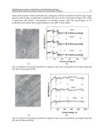
further, Fig.10 shows the simulated IRR results for different polyphase networks with
mismatch consideration. The IRR is illustrated in three-dimensional plot as a function of the
resistor’s electrical value (R) and resistor size, which for the current study corresponds to
the width (W). In the X-axis, the parameter R is used to calibrate the first stage of the
polyphase filter. The resistor values of the other stages are set to a fixed pole ratio α, as
shown in (14). The capacitors are chosen to give the right pole frequency.
These three-dimensional plots show first that multiplying the number of stages gives a
higher IRR. For example for the couple (R, W) equal to (70Ω, 10µm), the IRR increases from
52dB with three-stage polyphase design (Fig.10(a)), to 60dB with four stages (Fig.10(b)) and
reaches 65dB with five stages (Fig.10(c)). However, having many stages in the polyphase
network conducts to a growth of the components number and increases the silicon area, the
power loss and the parasitic capacitances. Hence, according to the costumer need, designers
should make a compromise between achieving a polyphase filter with high image rejection
and low area and low silicon area cost.
Furthermore, Fig.10 illustrates that a high IRR is achieved if the value and the size of the
resistor converge to the optimal values on each multi-stage polyphase filter. For about the
different filter configurations, it shows that the IRR variation versus R corresponding to a
given configuration is quasi-linear. For instance for a five-stage PPF, the IRR changes from
65dB, to 68dB and 70dB for resistor’s width of 10µm, 20µm and 40µm respectively
(Fig.10(c)). In this case, it can be noted that a gain of only 5dB in the IRR produces an
expansion of the resistor size by almost 400% confirming the existence of an optimal
component sizing for a specified IRR with each polyphase filter configuration. The possible
reason is that large component area yields better matching on the circuit and presents
optimal parasitic capacitances effect.
(a) (b)
30
60
90
120
150
180
210
25
30
35
40
45
50
55
60
65
10
20
30
40
50
60
I
R
R
(
d
B
)
W
(µ
m
)
R
(
)
25,00
30,00
35,00
40,00
45,00
50,00
55,00
60,00
65,00
30
60
90
120
150
180
210
45
50
55
60
65
70
10
20
30
40
50
60
I
R
R
(
d
B
)
W
(
µ
m)
R
(
)
44,00
47,50
51,00
54,50
58,00
61,50
65,00
68,50
72,00
MobileandWirelessCommunications:Networklayerandcircuitleveldesign232
(c)
Fig. 10. IRR variation of (a) three, (b) four, and (c) five PPF versus resistor’s sizes and values
A statistical representation is suitable to characterize the processes happening in
probabilistic ways. In statistical simulations, sequences of random numbers with a certain
probability distribution function are used to model the stochastic process. Usually, many
statistical simulations runs are conducted and averaged to reach good accuracy of the
simulation results. Process tolerances and component mismatch in integrated circuits are
consequences of stochastic processes within a certain range, and they are usually available
in CMOS process files derived by elaborate measurements. It is known that both process
tolerances and component mismatch have truncated Gaussian probability distribution
functions (Spence & Soin, 1997). In our application, Monte Carlo simulation can be applied
to verify the statistical nature of the IRR with certain process tolerances and a resultant
component mismatch, and to check the probability distribution of the gain mismatch. After
optimal sizing and value calibrations of the PPF components as shown previously, three,
four and five stages are simulated. The analysis concerns the process and mismatch
variations of the PPF component corners (Polysilicon resistors and MIM (Metal-Insulator-
Metal) capacitors for the current study) before parasitics extraction on the frequency band
[2, 3] GHz. The Monte Carlo simulation results are expressed as frequency of occurrence
histogram (5050 samples of RF PPFs) for different intervals of the IRR and shown in Fig. 11.
(a) (b) (c)
Fig. 11. Monte Carlo simulation results of (a) three, (b) four and (c) five stage RF PPF: IRR
histogram (process and mismatch variations)
30
60
90
120
150
180
210
50
55
60
65
70
10
20
30
40
50
60
I
R
R
(
d
B
)
W
(
µ
m
)
R
(
)
50,00
53,00
56,00
59,00
62,00
65,00
68,00
71,00
74,00
30 40 50 60 70 80 90 100
0
200
400
600
800
1000
1200
1400
1600
1800
Number of samples
IRR (dB)
IRR histogram
Ideal Gaussian
40 50 60 70 80 90 100
0
200
400
600
800
1000
1200
1400
Number of samples
IRR (dB)
IRR histogram
Ideal Gaussian
60 70 80 90 100 110
0
200
400
600
800
1000
1200
1400
1600
Number of samples
IRR (dB)
IRR histogram
Ideal Gaussian
PolyphaseFilterDesignMethodologyforWirelesscommunicationApplications 233
(c)
Fig. 10. IRR variation of (a) three, (b) four, and (c) five PPF versus resistor’s sizes and values
A statistical representation is suitable to characterize the processes happening in
probabilistic ways. In statistical simulations, sequences of random numbers with a certain
probability distribution function are used to model the stochastic process. Usually, many
statistical simulations runs are conducted and averaged to reach good accuracy of the
simulation results. Process tolerances and component mismatch in integrated circuits are
consequences of stochastic processes within a certain range, and they are usually available
in CMOS process files derived by elaborate measurements. It is known that both process
tolerances and component mismatch have truncated Gaussian probability distribution
functions (Spence & Soin, 1997). In our application, Monte Carlo simulation can be applied
to verify the statistical nature of the IRR with certain process tolerances and a resultant
component mismatch, and to check the probability distribution of the gain mismatch. After
optimal sizing and value calibrations of the PPF components as shown previously, three,
four and five stages are simulated. The analysis concerns the process and mismatch
variations of the PPF component corners (Polysilicon resistors and MIM (Metal-Insulator-
Metal) capacitors for the current study) before parasitics extraction on the frequency band
[2, 3] GHz. The Monte Carlo simulation results are expressed as frequency of occurrence
histogram (5050 samples of RF PPFs) for different intervals of the IRR and shown in Fig. 11.
(a) (b) (c)
Fig. 11. Monte Carlo simulation results of (a) three, (b) four and (c) five stage RF PPF: IRR
histogram (process and mismatch variations)
30
60
90
120
150
180
210
50
55
60
65
70
10
20
30
40
50
60
I
R
R
(
d
B
)
W
(
µ
m
)
R
(
)
50,00
53,00
56,00
59,00
62,00
65,00
68,00
71,00
74,00
30 40 50 60 70 80 90 100
0
200
400
600
800
1000
1200
1400
1600
1800
Number of samples
IRR (dB)
IRR histogram
Ideal Gaussian
40 50 60 70 80 90 100
0
200
400
600
800
1000
1200
1400
Number of samples
IRR (dB)
IRR histogram
Ideal Gaussian
60 70 80 90 100 110
0
200
400
600
800
1000
1200
1400
1600
Number of samples
IRR (dB)
IRR histogram
Ideal Gaussian
The impact of process and mismatch variations on the PPF response is summarized in table
3. It illustrates the worst case and mean value of IRR, as well as the notch position drift and
the IRR distribution between 50dB and 90dB.
P
PF sta
g
es
number
M
ean value
of the IRR
Worst
case IRR
N
otch
drift
Standard
deviation σ
IRR distribution
between 50dB and
90dB
3 62dB 51dB 405MHz 9.11 85%
4 72dB 57dB 306MHz 10.05 95%
5 87dB 64dB 317MHz 11.95 97%
Table 3. Monte Carlo simulation results of multi-stage RF PPFs: mean value and worst case
IRR, notch position drift and IRR distribution between 50dB and 90dB
The obtained results confirm that increasing the stages number increases the mean value of
the IRR on the desired bandwidth. It can be noted that the higher is the PPF stages number,
the lower is the PPF immunity to mismatch effects, given that the distribution becomes
wider and the standard deviation σ increases from 9.11 to 10.05 and 11.95 for three-stage,
four-stage and five-stage RF PPFs respectively. This is due to the components and
connections growth in the design, inducing, at the same time, an expansion of its area.
Let us consider a unit surface S
0
of a one-stage RF PPF. Since in the RF domain the size of
our PPF components is almost identical, we can suppose that an n-stage PPF has a surface of
n.S
0
. Thus, a compromise can be made while designing PPFs depending on the system
specifications. For example, a 60dB image rejection will cost 3.S
0
with a standard deviation
of 9, while a roughly 85dB image rejection will cost 5.S
0
with a standard deviation of 12.
6. Parasitics analysis and line modeling
Since the implementation of RC polyphase filter on integrated circuit engenders parasitic
capacitance to the substrate and at the output nodes, special attention must to be paid on the
parasitic capacitance and loading capacitance effects. In Fig.12 we model a simplified
equivalent circuit of a two-stage RC PPF with parasitic capacitance to substrate (Cp1, Cp2,
Cp3) and load capacitance (a part of Cp3).
MobileandWirelessCommunications:Networklayerandcircuitleveldesign234
Fig. 12. Equivalent circuit of the two-stage RC PPF with parasitic capacitance
In this case, the transfer functions of one-stage and two-stage RC polyphase filter are given
respectively as follows
(18)
(19)
It can be noted from (18) and (19) that the parasitic capacitances do not change the zero
positions 1/2πR
1
C
1
and 1/2πR
2
C
2
of H
p1
(jω) and H
p2
(jω). Simulation results of frequency
response including parasitic capacitances depict that the gain drops for high frequency
domain when the parasitic capacitance values increase (Yamaguchi et al, 2003).
Furthermore, properly arranging the components and optimally sizing the connections are
necessary to guarantee an equilibrated parasitic repartition in the circuit, which can
conserve the symmetrical structure of passive polyphase filter. The major loss and parasitic
capacitance contributions in connections are considered in order to obtain better filter
performance. In fact, loss in a conductor can be generally described by the following
equation
(20)
where ρ
film
is the thin film resistivity of the metal, t is the metal thickness, and L and W are
the trace length and width, respectively. Therefore, loss can be minimized by using metals
with very low resistivity, increasing the cross sectional area of the trace (t.W), or reducing
the overall trace length. Besides, the metal of connection is isolated from the semiconductor
substrate (typically at ground potential) by one or more dielectric layers used to separate
interconnect layers (inter-metal dielectrics). This creates a parasitic shunt capacitor that can
be approximated by the following equation
C1
C1
C1
C1
R1
R1
R1
R1
C2
C2
C2
C2
R2
R2
R2
R2
C
p2
C
p1
C
p1
C
p2
C
p1
C
p2
C
p1
C
p2
C
p3
C
p3
C
p3
C
p3
I
in
+
Q
in
+
I
in
-
Q
in
-
I
out
+
Q
out
+
I
out
-
Q
out
-
PolyphaseFilterDesignMethodologyforWirelesscommunicationApplications 235
Fig. 12. Equivalent circuit of the two-stage RC PPF with parasitic capacitance
In this case, the transfer functions of one-stage and two-stage RC polyphase filter are given
respectively as follows
(18)
(19)
It can be noted from (18) and (19) that the parasitic capacitances do not change the zero
positions 1/2πR
1
C
1
and 1/2πR
2
C
2
of H
p1
(jω) and H
p2
(jω). Simulation results of frequency
response including parasitic capacitances depict that the gain drops for high frequency
domain when the parasitic capacitance values increase (Yamaguchi et al, 2003).
Furthermore, properly arranging the components and optimally sizing the connections are
necessary to guarantee an equilibrated parasitic repartition in the circuit, which can
conserve the symmetrical structure of passive polyphase filter. The major loss and parasitic
capacitance contributions in connections are considered in order to obtain better filter
performance. In fact, loss in a conductor can be generally described by the following
equation
(20)
where ρ
film
is the thin film resistivity of the metal, t is the metal thickness, and L and W are
the trace length and width, respectively. Therefore, loss can be minimized by using metals
with very low resistivity, increasing the cross sectional area of the trace (t.W), or reducing
the overall trace length. Besides, the metal of connection is isolated from the semiconductor
substrate (typically at ground potential) by one or more dielectric layers used to separate
interconnect layers (inter-metal dielectrics). This creates a parasitic shunt capacitor that can
be approximated by the following equation
C1
C1
C1
C1
R1
R1
R1
R1
C2
C2
C2
C2
R2
R2
R2
R2
C
p2
C
p1
C
p1
C
p2
C
p1
C
p2
C
p1
C
p2
C
p3
C
p3
C
p3
C
p3
I
in
+
Q
in
+
I
in
-
Q
in
-
I
out
+
Q
out
+
I
out
-
Q
out
-
ܥൌ
ܣǤߝ
݀
(21)
where A is the total area of the metal traces, ε is the permittivity, and d is the thickness of the
dielectric. The parasitic capacitance decreases with high metals levels, but at the same time
this will increase the parasitic resistance because of stacking the different “via” resistivities.
Hence, designers must balance both the parasitic shunt capacitance and conductor loss
when selecting a conductor dimensions and metals levels.
Characterization and modeling of the interconnection lines have been performed to improve
their properties. The equivalent network line model between two ports used in this study is
shown in Fig.13(a). First, the line parameters have been extracted with electromagnetic
simulations (HFSS
TM
). Then, the correspondent line models have been specified and inserted
inside the polyphase filter design at the main sensitive points and simulated with the Agilent
ADS
®
tool. Calibration of the additional parasitics allows their allocation symmetrically
along the design, since their total elimination is not possible. This study has demonstrated
that lines with different shapes give the same filter response (IRR and bandwidth) provided
that the interconnect lengths in respectively I/Q paths are equalized. It is caused by the fact
that this will balance the parasitic interconnect resistance in each branch. For example,
serpentine and bus shapes could be used simultaneously for the parallel interconnections.
By adjusting the height of serpentine, the wire length in the branches of the PPF may be
equalized while keeping the same number of corners (Fig 13(b)).
(a) (b)
Fig. 13. (a) Equivalent network line model between different levels of interconnect. (b)
Considerations of interconnect to balance parasitics in polyphase filter branches
Besides, the inaccuracy of resistors and capacitors, due to Si substrate parasitic effect, causes
quadrature phase imbalance. To overcome this problem it is possible to make the polyphase
filter tunable so as to compensate the phase imbalance. The tunable phase can be used to
improve image rejection or moderate I/Q phase error in direct conversion or low-IF
receivers. For instance, varactor-based tunable polyphase filters on Si have been
implemented at 5GHz (Sanderson et al, 2004). Another technique to solve RC inaccuracy of
PPF is to use InGa/GaAs heterojunction bipolar transistor which has a very good frequency
response but which remains expensive (Meng et al, 2005). In addition, in the RF front-end
receiver, the input large parasitic capacitances of the following double quadrature mixer
degrade the loss of the RF polyphase filter. To overcome this problem, on-chip spiral
inductors are inserted at the output of the RF PPF in (Kim & Lee, 2006) and then tune out
the total input parasitic capacitances of the double quadrature mixer.
In our design, a new polyphase filter implementation (shown in Fig.14) is proposed to
balance the bandwidth variation due to mismatches in a symmetrical structure. It consists
on the RC basic passive polyphase network, adding up active resistors implemented with
MOS transistors. It is known that the R
on
of the MOS transistor is function of its dimensions
L
R
G
C
Port 1 Port 2
MobileandWirelessCommunications:Networklayerandcircuitleveldesign236
and of the grid voltage (VG). Thus, with an external tuning of VG, the value of R
on
, and then
the PPF resistor value and the notches, can be adjusted independently. Consequently, that
gives a tuning characteristic to the filter bandwidth, and can be applied to synthesize multi-
standards application filters. The MOS transistor dimensions are chosen to have the
adequate calibration of the bandwidth dispersion. Using these MOS active resistors possibly
adds nonlinearity to the PPF design, and then other active resistor realizations, such as
parallel-MOS and double-MOS differential resistor, with better linearity performance, have
been proposed (Allen & Holberg, 2002).
Fig. 14. Four-stage voltage tunable RC polyphase filter structure
7. Layout techniques
In addition, while components with large areas decrease the impact of mismatch, the
parasitic capacitance and resistance can have a much larger effect on output imbalance.
Minimization of these parasitics requires careful attention to layout symmetry. The parasitic
extraction procedure, performed with the Star-RCXT tool of Synopsys, shows that most
extracted parasitics are set in the interconnection network. Interconnects present electrical
losses that need to be taken into account during layout and then during performances
estimation. It is clear that, on the circuit, the inner traces see parasitic capacitance from the
left and right, while the outer traces only see parasitic capacitance from one side. Hence,
weaving the traces gives each path the same total distance spent as both an inner and an
outer trace. To equalize the parasitic effect of overlapping traces, a grid of vertical and
horizontal running interconnects has been laid out. Moreover, two parallel signal lines are
placed far enough apart so that the interline capacitance is negligible.
Furthermore, a judicious choice of metal level and interconnection drawing is necessary. In
fact, using high level of metallization engenders low parasitic capacitance but gives high
parasitic resistance. Thus, depending on the device sensibility and on the required matched
components, the metal level is chosen. For example, in low-loss applications, the metal 6 is
the most suitable (in 0.13µm CMOS technology) since it is the thickest one and has less
capacitance. The number of “vias” used for interconnects is also significant in leading to
equilibrated parasitics, especially in the case of RF passive polyphase filters. These vias give
R1
C1
C1
C1
C1
R1
R1
R1
R2
C2
C2
C2
C2
R2
R2
R2
R3
C3
C3
C3
C3
R3
R3
R3
R4
C4
C4
C4
C4
R4
R4
R4
VG4VG3VG2VG1
I
in
+
Q
in
+
I
in
-
Q
in
-
I
out
+
Q
out
+
I
out
-
Q
out
-
PolyphaseFilterDesignMethodologyforWirelesscommunicationApplications 237
and of the grid voltage (VG). Thus, with an external tuning of VG, the value of R
on
, and then
the PPF resistor value and the notches, can be adjusted independently. Consequently, that
gives a tuning characteristic to the filter bandwidth, and can be applied to synthesize multi-
standards application filters. The MOS transistor dimensions are chosen to have the
adequate calibration of the bandwidth dispersion. Using these MOS active resistors possibly
adds nonlinearity to the PPF design, and then other active resistor realizations, such as
parallel-MOS and double-MOS differential resistor, with better linearity performance, have
been proposed (Allen & Holberg, 2002).
Fig. 14. Four-stage voltage tunable RC polyphase filter structure
7. Layout techniques
In addition, while components with large areas decrease the impact of mismatch, the
parasitic capacitance and resistance can have a much larger effect on output imbalance.
Minimization of these parasitics requires careful attention to layout symmetry. The parasitic
extraction procedure, performed with the Star-RCXT tool of Synopsys, shows that most
extracted parasitics are set in the interconnection network. Interconnects present electrical
losses that need to be taken into account during layout and then during performances
estimation. It is clear that, on the circuit, the inner traces see parasitic capacitance from the
left and right, while the outer traces only see parasitic capacitance from one side. Hence,
weaving the traces gives each path the same total distance spent as both an inner and an
outer trace. To equalize the parasitic effect of overlapping traces, a grid of vertical and
horizontal running interconnects has been laid out. Moreover, two parallel signal lines are
placed far enough apart so that the interline capacitance is negligible.
Furthermore, a judicious choice of metal level and interconnection drawing is necessary. In
fact, using high level of metallization engenders low parasitic capacitance but gives high
parasitic resistance. Thus, depending on the device sensibility and on the required matched
components, the metal level is chosen. For example, in low-loss applications, the metal 6 is
the most suitable (in 0.13µm CMOS technology) since it is the thickest one and has less
capacitance. The number of “vias” used for interconnects is also significant in leading to
equilibrated parasitics, especially in the case of RF passive polyphase filters. These vias give
R1
C1
C1
C1
C1
R1
R1
R1
R2
C2
C2
C2
C2
R2
R2
R2
R3
C3
C3
C3
C3
R3
R3
R3
R4
C4
C4
C4
C4
R4
R4
R4
VG4VG3VG2VG1
I
in
+
Q
in
+
I
in
-
Q
in
-
I
out
+
Q
out
+
I
out
-
Q
out
-
high contact resistance that can be almost equal to the filter resistance. Table 4 presents some
extraction results of a line connection between a resistor and a capacitor having different
metal levels with different vias number. It shows that increasing the number of vias does
not change the parasitic capacitance, but decreases the parasitic resistance. It is due to
putting the contact resistance of each via in parallel and then lowering the equivalent
resistance. Therefore, connections in the radio frequency PPF have to use great number of
vias to minimize their parasitic effect.
M
etal level o
f
the line
Via number
P
arasitic
capacitance (fF)
P
arasitic
Resistance (Ω)
Metal 2
1 14.5 19.11
2 14.54 11
3 14.56 7
Metal 3
1 14.13 19.11
2 14.15 13.49
3 14.18 10.82
Table 4. Extraction results of a line connection (W=2.5-µm/L=5-µm) with different metal
levels between a Polysilicon-resistor and a MIM-capacitor in 0.13µm CMOS technology
Total equilibrated interconnects drawing is hard to obtain in the case of PPF. However,
owing to the symmetry of the PPF stages, the parasitic modelling and extraction procedures
illustrate that ensuring the same drawings between I and Q paths is sufficient to guarantee
same matching and same performances as in the case of an ideal structure (with same
drawings for the four PPF paths), and then, that may loosen the constraints of design
techniques.
In addition to designing a symmetrical circuit, further layout techniques have been used to
assure highly matched devices, as shown below
To reduce the sensitivity of the device to process biases, resistors are made same width
and capacitors consider same area-to-periphery ratios.
Dummy resistors are added to either border of an array of matched resistors to
guarantee uniform etching. Dummies should be electrically connected to ground (or to
other low-impedance node) to avoid electrostatic modulation and floating diffusions.
Moreover, the metal overlapping the active area of resistors can lead to metallization-
induced mismatches. Thus, the “folded-out” interconnection (Fig.15(a)) produces better
matching than the “folded-in” interaction (Fig.15(b)).
Stress has an impact upon silicon since it is piezoresistive. One of the most known
techniques for reducing stress-induced mismatches is the common-centroid layout. It
arranges segments of matched devices along one dimension. For example, if we consider
two devices (A and B), each composed of two segments, the possible patterns are shown
in Fig.15(c). The pattern ABBA has an axis of symmetry that divides it into two mirror-
image halves (AB and BA). It requires dummies since segments of A occupy both ends of
the array. The pattern ABAB, with interdigitated resistors, haven’t common axis of
symmetry and needs dummies as well as the ABBA pattern. Thus, the pattern ABAB lets
stress-induced mismatches on devices and consequently it should be avoided (Hastings,
2006).
MobileandWirelessCommunications:Networklayerandcircuitleveldesign238
Thermoelectric effects cannot be eliminated with the common-centroid layout in the case
of an array of resistors, because they arise from differences in temperature between the
ends of each resistor segment. The thermoelectric potentials of individual segments can
be cancelled by reconnecting them as shown in Fig.15(d). The resistor should have an
even number of segments, half connected in one direction and half connected in the
other.
Electrostatic interactions cause variations in resistors and capacitances. Thus, matched
resistors with same values can belong to a common tank (or N-wells). If resistors have
different values, they should be divided into segments of equal values, and each
segment must reside in its own independently biased tank. In addition, wires that do not
connect matched resistors should not cross them, because they may capacitively couple
noise into the resistor and the electric field between the wire and the resistor can
modulate the conductivity of the resistance material. The electrostatic shielding (or Faraday
shielding) is a technique that can isolate a resistor from the influence of overlying leads
and gives shielding against capacitive coupling (Hastings, 2006).
To avoid electromigration between signals, I and Q paths are separated with a grounded
bus.
Size, orientation and temperature stress of MOS transistors influence their matching. A
better matching is obtained when transistors are oriented along the same crystal axis in
the same direction because of the stress-induced mobility variations. They should also be
placed in close proximity even next to one another in order to facilitate common-
centroid layout.
(a) (b) (c) (d)
Fig. 15. Resistor array interconnection in (a) “folded-in” and (b) “folded-out” styles. (c)
Examples of common-centroid arrays. (d) Proper connection of resistor segments
cancelling the thermoelectric
8. PPF Design methodology
As analyzed previously, component mismatch, process tolerances and parasitic effects must
be considered in the design of CMOS PPFs to accomplish a robust design. We propose a
design methodology dedicated to PPFs as shown in Fig.16. Such top-down design
methodology is a structured approach to design PPFs operating from wide frequency range
and which can satisfy high performances in terms of IRR (about 60dB) from wide frequency
range (1MHz to 5GHz).
This PPF design methodology can be arranged into considerations first in the system
requirements, then in the schematic design and next in the layout view. Thus, starting out
from target specifications and constraints in terms of IRR, application bandwidth, cost and
consumption, we can summarize the design flow as the guidelines below
R1 R2 R2 R1
R1 R2 R2 R1
A ABB
A BAB
+ + + +
- - - -
PolyphaseFilterDesignMethodologyforWirelesscommunicationApplications 239
Thermoelectric effects cannot be eliminated with the common-centroid layout in the case
of an array of resistors, because they arise from differences in temperature between the
ends of each resistor segment. The thermoelectric potentials of individual segments can
be cancelled by reconnecting them as shown in Fig.15(d). The resistor should have an
even number of segments, half connected in one direction and half connected in the
other.
Electrostatic interactions cause variations in resistors and capacitances. Thus, matched
resistors with same values can belong to a common tank (or N-wells). If resistors have
different values, they should be divided into segments of equal values, and each
segment must reside in its own independently biased tank. In addition, wires that do not
connect matched resistors should not cross them, because they may capacitively couple
noise into the resistor and the electric field between the wire and the resistor can
modulate the conductivity of the resistance material. The electrostatic shielding (or Faraday
shielding) is a technique that can isolate a resistor from the influence of overlying leads
and gives shielding against capacitive coupling (Hastings, 2006).
To avoid electromigration between signals, I and Q paths are separated with a grounded
bus.
Size, orientation and temperature stress of MOS transistors influence their matching. A
better matching is obtained when transistors are oriented along the same crystal axis in
the same direction because of the stress-induced mobility variations. They should also be
placed in close proximity even next to one another in order to facilitate common-
centroid layout.
(a) (b) (c) (d)
Fig. 15. Resistor array interconnection in (a) “folded-in” and (b) “folded-out” styles. (c)
Examples of common-centroid arrays. (d) Proper connection of resistor segments
cancelling the thermoelectric
8. PPF Design methodology
As analyzed previously, component mismatch, process tolerances and parasitic effects must
be considered in the design of CMOS PPFs to accomplish a robust design. We propose a
design methodology dedicated to PPFs as shown in Fig.16. Such top-down design
methodology is a structured approach to design PPFs operating from wide frequency range
and which can satisfy high performances in terms of IRR (about 60dB) from wide frequency
range (1MHz to 5GHz).
This PPF design methodology can be arranged into considerations first in the system
requirements, then in the schematic design and next in the layout view. Thus, starting out
from target specifications and constraints in terms of IRR, application bandwidth, cost and
consumption, we can summarize the design flow as the guidelines below
R1 R2 R2 R1
R1 R2 R2 R1
A ABB
A BAB
+ + + +
- - - -
Accomplishing analytical calculations and modeling to quantify the component
mismatch and parasitic elements effects and to focus on the resulting PPF response to
phase and gain imbalances.
Fixing the number of stages needed for the polyphase filter according to the bandwidth
to be covered and the desirable image rejection amount.
Equally placing the notches on the frequency domain with growing impedance while
traversing the filter stages to lower losses and noise figure.
If the cascade filter loss is still too large, we move on changing the component type as well
as calibrating its parameters, even as inserting inter-stage buffers to preserve signal dynamic
range within the polyphase filter. After adjusting the losses into the PPF, we fulfill statistical
simulations to longer analyze the component mismatch.
Optimal sizing of the PPF components in terms of electrical value and dimensions. The
matching quantities needed between resistors and capacitors determine the physical area
of the filter.
If in the schematic simulation, the target specification cannot be met, we move on to the
component resizing procedure and deduce the compliance with the required constraints.
After completing the schematic design, we carry out the physical layout design.
Modeling the interconnection lines and performing electromagnetic simulation to
deduce their parameters; and then inserting them in the PPF design to maximize its
immunity to the non idealities.
Designing the layout taking into account the parasitic elements: the conductor loss of the
interconnect metal creates parasitic resistance, and the dielectric between the traces and
the substrate or between two overlapping traces creates parasitic capacitance. Layout
which creates equal parasitics for each path through the polyphase is necessary to
minimize the imbalance and maintain the symmetry.
Using dummies around the matched components to reduce the boundary effects and on-
chip shielding to isolate the PPF design from the unwanted substrate noise coupling. The
electromigration is minimized with a ground separation between the I and Q signals. A
judicious choice of the metal level and number of contacts or vias is also necessary.
Post layout simulating the PPF with the extracted coefficients. In this extraction method,
parasitics between neighboring components, wires and parasitics to the substrate are
extracted. In this way, we can provide realistic simulation results before manufacturing
the circuit.
If the target specifications required by the application are not yet satisfied, we go back to the
parasitics minimization procedure and post-layout simulation (PLS) until assuring them.
Then, we finish the design.
MobileandWirelessCommunications:Networklayerandcircuitleveldesign240
Fig. 16. High performance PPF design planning flow
9. PPF implementation
The proposed design methodology has been validated with some test-cases in full CMOS
process. For instance, Fig.17 shows the layout of a four-stage RF tunable PPF (rf. Fig.14)
designed to work around 5GHz, and fabricated in 0.13-µm CMOS technology. It occupies a
die area of 310 x 83 µm² without test pads.
Fig. 17. Layout of the 5GHz four-stage tunable PPF: 310 x 83 µm² without test pads
Designconstraints
(IRR,BW,cost,consumption)
Analytical modeling
(mismatchestimation)
Calibrationof
ElectricalvalueofR,C
(notches,NF,losses)
Choosesuitable
Componenttypevs.
Processdrift(PVT)
(IRR,BW,area,consumption)
NFandlosses
minimized
No
Yes
Mismatchanalysis
(Monte‐Carloand
Resizing)
Optimal
components
valueandsize
Drawingtechniques
(size,orientation,symmetry)
Dummies&Shields
Interconnectparasitics
minimization (PLS*)
(vias,wires,metallevel)
Electromigration
techniques
(I/Qsignalsseparation)
No
Yes
SuitableIRR
forapplication
No
System requirement
Schematic
Layout
* PLS: Post Layout Simulation
End
Yes
Linesmodeling
(Electromagnetic
simulation)
R
C
MOS
PolyphaseFilterDesignMethodologyforWirelesscommunicationApplications 241
Fig. 16. High performance PPF design planning flow
9. PPF implementation
The proposed design methodology has been validated with some test-cases in full CMOS
process. For instance, Fig.17 shows the layout of a four-stage RF tunable PPF (rf. Fig.14)
designed to work around 5GHz, and fabricated in 0.13-µm CMOS technology. It occupies a
die area of 310 x 83 µm² without test pads.
Fig. 17. Layout of the 5GHz four-stage tunable PPF: 310 x 83 µm² without test pads
Designconstraints
(IRR,BW,cost,consumption)
Analytical modeling
(mismatchestimation)
Calibrationof
ElectricalvalueofR,C
(notches,NF,losses)
Choosesuitable
Componenttypevs.
Processdrift(PVT)
(IRR,BW,area,consumption)
NFandlosses
minimized
No
Yes
Mismatchanalysis
(Monte‐Carloand
Resizing)
Optimal
components
valueandsize
Drawingtechniques
(size,orientation,symmetry)
Dummies&Shields
Interconnectparasitics
minimization (PLS*)
(vias,wires,metallevel)
Electromigration
techniques
(I/Qsignalsseparation)
No
Yes
SuitableIRR
forapplication
No
System requirement
Schematic
Layout
* PLS: Post Layout Simulation
End
Yes
Linesmodeling
(Electromagnetic
simulation)
R
C
MOS
The frequency response of the implemented 5GHz tunable PPF is depicted in Fig.18. It
shows that the variation of the control grid voltage of MOS resistors enables the tuning of
the PPF bandwidth by 1GHz while conserving an IRR almost steady around 75dB. Then,
this proposed tuning characteristic can be applied to multi-standard applications, or used to
compensate for the bandwidth drift due to mismatches.
Fig. 18. Frequency responses of the 5GHz tunable polyphase filters using different control
grid voltages
A chip photo of the fabricated chip is shown in Fig.19. It occupies 815 x 319 µm² with test
pads. On-chip polysilicon resistors have been added to recombine the four outputs of the
PPF in order to avoid the inaccuracy of the external hybrid couplers and to facilitate the
measurement procedure. Thus, a differential output is obtained and can be measured easily
with active probes.
Fig. 19. Die micrograph of the fabricated PPF test chip in 0.13-µm CMOS technology
3E9 4E9 5E9 6E9 7E9 8E9 9E9 1E10
-30
-40
Image Rejection (dB)
Frequency (Hz)
-40
-50
-60
-70
-80
0.3 V
0.6 V
0.9 V
1.2 V
PPF
Test pads G-S-G-S-G
MobileandWirelessCommunications:Networklayerandcircuitleveldesign242
Fig. 20. Diagram of the PPF measurement setup
A diagram of the measurement setup for test of the CMOS PPF is illustrated in Fig.20. On-
wafer RF measurements can be performed since balanced G-S-G-S-G pads (G for ground
and S for signal) are used. The four input phases of the filter are generated by using a signal
generator and wideband passive hybrid couplers. The measurement procedure is being
processed to validate the obtained simulation results.
10. Conclusion
Wireless communication bands and services are proliferating, resulting in a great
development of standards and in an enhanced need for integrated circuits. In this paper, it is
demonstrated that techniques for image rejection have been constantly evolving in recent
years because of this tremendous success of wireless products. Among the various
techniques, the polyphase filters might become the choice for future image rejection scheme,
thanks to its promising performances and to the semiconductor process advances. An
analytical approach of RC polyphase filters as well as a study of components mismatch and
non-ideality impact on the IRR degradation have been presented in this paper. That leads us
to propose a design methodology dedicated to passive polyphase filters (PPFs), taking into
account optimum component sizing, lines modeling and layout symmetry and matching.
This method has been validated with some test-cases in full CMOS technology and allows
attaining high image rejection (about 60dB) from wide frequency range (1MHz to 5GHz).
In addition, the wireless services have different carrier frequencies, channel bandwidths,
modulation schemes, data rates, etc., which motivates the industry to look for multi-
standard and multi-band devices. In this paper, a tunable polyphase filter structure has been
proposed, which can be applied to synthesize multi-standard application filters. This tuning
characteristic can be also used to compensate for the bandwidth drift due to mismatches.
0°
180°
90°
270°
0°
180°
RF PPF
Test Chip
RF
Cable
Active
probe
Hybrid Couplers
180°
90°
MOS VG control
180°
Spectrum
analyser
RF
generator
Active
probe
PolyphaseFilterDesignMethodologyforWirelesscommunicationApplications 243
Fig. 20. Diagram of the PPF measurement setup
A diagram of the measurement setup for test of the CMOS PPF is illustrated in Fig.20. On-
wafer RF measurements can be performed since balanced G-S-G-S-G pads (G for ground
and S for signal) are used. The four input phases of the filter are generated by using a signal
generator and wideband passive hybrid couplers. The measurement procedure is being
processed to validate the obtained simulation results.
10. Conclusion
Wireless communication bands and services are proliferating, resulting in a great
development of standards and in an enhanced need for integrated circuits. In this paper, it is
demonstrated that techniques for image rejection have been constantly evolving in recent
years because of this tremendous success of wireless products. Among the various
techniques, the polyphase filters might become the choice for future image rejection scheme,
thanks to its promising performances and to the semiconductor process advances. An
analytical approach of RC polyphase filters as well as a study of components mismatch and
non-ideality impact on the IRR degradation have been presented in this paper. That leads us
to propose a design methodology dedicated to passive polyphase filters (PPFs), taking into
account optimum component sizing, lines modeling and layout symmetry and matching.
This method has been validated with some test-cases in full CMOS technology and allows
attaining high image rejection (about 60dB) from wide frequency range (1MHz to 5GHz).
In addition, the wireless services have different carrier frequencies, channel bandwidths,
modulation schemes, data rates, etc., which motivates the industry to look for multi-
standard and multi-band devices. In this paper, a tunable polyphase filter structure has been
proposed, which can be applied to synthesize multi-standard application filters. This tuning
characteristic can be also used to compensate for the bandwidth drift due to mismatches.
0°
180°
90°
270°
0°
180°
RF PPF
Test Chip
RF
Cable
Active
probe
Hybrid Couplers
180°
90°
MOS VG control
180°
Spectrum
analyser
RF
generator
Active
probe
11. References
Allen, P. E. & Holberg, D. R. (2002). CMOS Analog circuit design (éd. 2nd). New York: Oxford
University Press.
Andreani, P.;
Mattisson, S. & Essink, B. (2000). A CMOS gm-C polyphase filter with high
image band rejection. Proceedings of the European Solid State Circuits Conference, 244-
247.
Andreani, P. & Mattison, S. (2002). On the use of Nauta's transconductor in low-frequency
CMOS gm-C bandpass filters. IEEE Journal of Solid State Circuits, 37, 114-124.
Banu, M.; Wang, H.; Seidel, M.; Tarsia, M.; Fischer, W.; Glas, J.; Dec, A. & Boccuzzi, V.
(1997). A BiCMOS Double low-IF receiver for GSM. Proceedings of IEEE Custom
Integrated Circuits Conference, 521-524.
Behbahani, F.; Kishigami, Y.; Leete, J. & Abidi, A. A. (1999). CMOS 10 MHz IF
downconverter with on-chip broadband circuit for large image suppression.
Symposium on VLSI circuits, 83-86.
Behbahani, F.; Weeguan, T.; Karimi-Sanjaani, A.; Roithmeier, A. & Abidi, A. A. (2000). A
broadband tunable CMOS channel select filter for a low-IF wireless receiver. IEEE
Journal of Solid State Circuits, 35 (4), 476-489.
Behbahani, F.; Kishigami, Y.; Leete, J. & Abidi, A. A. (2001). CMOS mixers and Polyphase
filters for large image rejection. IEEE Journal of Solid State Circuits, 36 (6), 873-887.
Behbahani, F.; Firouzkouhi, H.; Chokkalingam, R.; Delshadpour, S.; Kheirkhahi, A.;
Nariman, M.; Conta, M. & Bhatia, S. (2002). A fully integrated low-IF CMOS GPS
radio with on-chip analog image rejection. IEEE Journal of Solid State Circuits, 37
(12), 1721-1727.
Behzad, A.; Lin, L.; Shi, Z.M.; Anand, S.; Carter, K.; Kappes, M.; Lin, E.; Nguyen, T.; Yuan,
D.; Wu, S.; Wong, Y.C.; Fong, V. & Rofougaran, A. (2003). Direct conversion CMOS
transceiver with automatic frequency control for 802.11a wireless LANs. Solid State
Circuits Conference ISSCC, 1, 356-499.
Carta, C.; Vogt, R. & Bachtold, W. (2005). Multiband monolithic BiCMOS low-power low-IF
WLAN receivers. IEEE Microwave and Wireless Components Letters, 15 (9), 543-545.
Chian, L. et al. (2007). Design of tunable polyphase filter using MOSFET. Proceedings of the
International Symposium on Integrated Circuits, 349-352.
Chou, S. & Lee, H. (2007). Effect of phase mismatch on image rejection in Weaver
architecture. IEEE Microwave and Wireless components Letters, 17 (1), 70-72.
Chou, C. & Wu, C. (2005). The design of wideband and low-power CMOS active polyphase
filter and its application in RF double-quadrature receivers. IEEE Trans. on Circuits
and Systems I: Regular Papers, 52 (5), 825-833.
Crols, J. & Steyaert, M. (1995). A single chip 900 MHz CMOS receiver front-end with a high
performance low-IF topology. IEEE Journal of Solid State Circuits, 30 (12), 1483-1492.
Crols, J. & Steyaert, M. (1998). Low-IF topologies for high-performance analog font ends of
fully integrated receivers. IEEE Trans. on Circuits and Systems II, 45, 269-282.
Der, L. & Razavi, B. (2003). A 2 GHz CMOS Image-reject receiver with LMS calibration.
IEEE
Journal of Solid State Circuits, 38 (2), 167-175.
Elmala, M. & Embabi, S. (2004). Calibration of phase and gain mismatches in Weaver image-
reject receiver. IEEE Journal of Solid State Circuits, 39 (2), 283-289.
Fang, S. et al. (2005). An image rejection down converter for low-IF receivers. IEEE Trans. on
Microwave Theory and Techniques, 53 (2), 478-487.
MobileandWirelessCommunications:Networklayerandcircuitleveldesign244
Galal, S. H.; Ragaie, H. F. & Tawfik, M. S. (2000). RC sequence asymmetric polyphase
networks for RF integrated transceivers. IEEE Trans. on circuits and Systems II, 47 (1),
1127-1134.
Galal, S. H. & Tawfik, M. S. (1999). On the design and sensitivity of RC sequence asymmetric
polyphase networks in RF integrated transceiver. Proceedings of IEEE International
Symposium on Circuit and System, 2, 593-597.
Gingell, M. (1971). Brevet n° 3,559,042; 3,618,133. US patents.
Harrison, J. (2002). 350 MHz opamp-RC filter in 0.18 µm CMOS. Electron Letters, 38 (6), 259-
260.
Hastings, A. (2006). The art of analog design. New Jersey: Prentice Hall, 2
nd
Edition.
Huang, Q.; Orsatti, P. & Piazza, F. (1999). GSM transceiver front-end circuits in 0.25 µm
CMOS. IEEE Journal of Solid State Circuits, 34 (3), 292-303.
Khvedelidze, B. (2001). Hilbert transform. Dans M. Hazewinkel, Encyclopaedia of
Mathematics. Netherlands: Kluwer Academic Publishers.
Kim, C. & Lee, S. (2006). A 5.25 GHz image rejection RF front-end receiver with polyphase
filters. IEEE Microwave and Wireless Components Letters, 16 (5), 302-304.
Komoriyama, K; Yashiki, M.; Yoshida, E. & Tanimoto, H. (2007). A very wideband fully
balanced active RC polyphase filter based on CMOS inverters in 0.18 µm CMOS
technology. Proceedings of Symposium on VLSI Circuits, 89-99.
Lee, S.; Jung, K.; Kim, W.; Ryu, H. & Song, W. (1998). A 1 GHz image-rejection
downconverter in 0.8 µm CMOS technology. IEEE Trans. on Customer Electronics, 44
(2), 235-239.
Lee, T.H.; Samavati, H. & Rategh, H.R. (2002). 5 GHz CMOS Wireless LANs. IEEE Trans. on
Microwave and Theory Techniques, 50 (1), 268-280.
Lerstaveesin, S. & Song, B. (2006). A complex image rejection circuit with Sign detection
only. IEEE Journal of Solid State Circuits, 41 (12), 2693-2702.
Long, J. R. (1996). A narrowband radio receiver front-end portable communications
applications. Ph.D dissertation . Carleton University.
Long, J. R. & Maliepaard, M. (1999). A 1V 900 MHz image-reject downconverter in 0.5 µm
CMOS. IEEE Custom Integrated Circuits Conference, 665-668.
Macedo, J. A., & Copeland, M. A. (1998). A 1.9 GHz Silicon Receiver with monolithic image
filtering. IEEE Journal of Solid State Circuits, 33 (3), 378-386.
Maligeorgos, J. & Long, J. (2000). A 2V 5.1-5.8 GHz Image-reject receiver with wide dynamic
range. IEEE Solid-State Circuits Conference ISSCC, 322-323.
McNutt, M.J.; LeMarquis, S. & Dunkley, J.L. (1994). Systematic capacitance matching errors
and corrective layout procedures. IEEE Journal of Solid State Circuits, 29 (5), 611-616.
Meng, C.C.; Sung, D.W. & Huang, G.W. (2005). 5.2 GHz GaInP/GaAs HBT double-
quadrature downconverter with polyphase filters for 40 dB image rejection. IEEE
Microwave and Wireless Components Letters, 15 (2), 59-61.
Mikkelsen, J. H. (1998). Evaluation of CMOS front-end receiver architectures for GSM
handset applications. IEEE Symp. Communications Systems and Digital Signal
Processing, 164-167.
Montemayor, R. & Razavi, B. (2000). A self-calibrating 900 MHz image reject receiver.
Proceedings of ESSCIRC, 292-295.
Razavi, B. (1996). Challenges in portable RF transceiver design. IEEE Circuits and Devices
Magazine, 12, 12-25.
PolyphaseFilterDesignMethodologyforWirelesscommunicationApplications 245
Galal, S. H.; Ragaie, H. F. & Tawfik, M. S. (2000). RC sequence asymmetric polyphase
networks for RF integrated transceivers. IEEE Trans. on circuits and Systems II, 47 (1),
1127-1134.
Galal, S. H. & Tawfik, M. S. (1999). On the design and sensitivity of RC sequence asymmetric
polyphase networks in RF integrated transceiver. Proceedings of IEEE International
Symposium on Circuit and System, 2, 593-597.
Gingell, M. (1971). Brevet n° 3,559,042; 3,618,133. US patents.
Harrison, J. (2002). 350 MHz opamp-RC filter in 0.18 µm CMOS. Electron Letters, 38 (6), 259-
260.
Hastings, A. (2006). The art of analog design. New Jersey: Prentice Hall, 2
nd
Edition.
Huang, Q.; Orsatti, P. & Piazza, F. (1999). GSM transceiver front-end circuits in 0.25 µm
CMOS. IEEE Journal of Solid State Circuits, 34 (3), 292-303.
Khvedelidze, B. (2001). Hilbert transform. Dans M. Hazewinkel, Encyclopaedia of
Mathematics. Netherlands: Kluwer Academic Publishers.
Kim, C. & Lee, S. (2006). A 5.25 GHz image rejection RF front-end receiver with polyphase
filters. IEEE Microwave and Wireless Components Letters, 16 (5), 302-304.
Komoriyama, K; Yashiki, M.; Yoshida, E. & Tanimoto, H. (2007). A very wideband fully
balanced active RC polyphase filter based on CMOS inverters in 0.18 µm CMOS
technology. Proceedings of Symposium on VLSI Circuits, 89-99.
Lee, S.; Jung, K.; Kim, W.; Ryu, H. & Song, W. (1998). A 1 GHz image-rejection
downconverter in 0.8 µm CMOS technology. IEEE Trans. on Customer Electronics, 44
(2), 235-239.
Lee, T.H.; Samavati, H. & Rategh, H.R. (2002). 5 GHz CMOS Wireless LANs. IEEE Trans. on
Microwave and Theory Techniques, 50 (1), 268-280.
Lerstaveesin, S. & Song, B. (2006). A complex image rejection circuit with Sign detection
only. IEEE Journal of Solid State Circuits, 41 (12), 2693-2702.
Long, J. R. (1996). A narrowband radio receiver front-end portable communications
applications. Ph.D dissertation . Carleton University.
Long, J. R. & Maliepaard, M. (1999). A 1V 900 MHz image-reject downconverter in 0.5 µm
CMOS. IEEE Custom Integrated Circuits Conference, 665-668.
Macedo, J. A., & Copeland, M. A. (1998). A 1.9 GHz Silicon Receiver with monolithic image
filtering. IEEE Journal of Solid State Circuits, 33 (3), 378-386.
Maligeorgos, J. & Long, J. (2000). A 2V 5.1-5.8 GHz Image-reject receiver with wide dynamic
range. IEEE Solid-State Circuits Conference ISSCC, 322-323.
McNutt, M.J.; LeMarquis, S. & Dunkley, J.L. (1994). Systematic capacitance matching errors
and corrective layout procedures. IEEE Journal of Solid State Circuits, 29 (5), 611-616.
Meng, C.C.; Sung, D.W. & Huang, G.W. (2005). 5.2 GHz GaInP/GaAs HBT double-
quadrature downconverter with polyphase filters for 40 dB image rejection. IEEE
Microwave and Wireless Components Letters, 15 (2), 59-61.
Mikkelsen, J. H. (1998). Evaluation of CMOS front-end receiver architectures for GSM
handset applications. IEEE Symp. Communications Systems and Digital Signal
Processing, 164-167.
Montemayor, R. & Razavi, B. (2000). A self-calibrating 900 MHz image reject receiver.
Proceedings of ESSCIRC, 292-295.
Razavi, B. (1996). Challenges in portable RF transceiver design. IEEE Circuits and Devices
Magazine, 12, 12-25.
Razavi (a), B. (1997). RF Microelectronics. New Jersey: Prentice Hall.
Razavi (b), B. (1997). Design considerations for direct conversion receivers. IEEE Trans.
Circuits and Systems II, 44 (6), 428-435.
Razavi, B. (2001). A 5.2 GHz CMOS receiver with 62 dB image rejection. IEEE Journal of Solid
State Circuits, 36 (5), pp.810-815.
Rudell, J. C.; Ou, J J.; Cho, T.B.; Chien, G.; Brianti, F.; Weldon, J.A. & Gray, P.R. (1997). A 1.9
GHz wideband IF double conversion CMOS receiver for cordless telephone
applications. IEEE Journal of Solid State Circuits, 32 (12), 2071-2088.
Samavati, H.; Rategh, H.R. & Lee, T.H. (2000). A 5 GHz CMOS Wireless LAN receiver front
end. IEEE Journal of Solid State Circuits, 35 (5), 765-772.
Samavati, H., & al., e. (2001). A fully integrated 5 GHz CMOS Wireless LAN receiver.
Proceedings of ISSCC, 208-209.
Sanderson, D. et al. (2004). A 5-6 GHz polyphase filter with tunable I/Q phase balance. IEEE
Tansactions on Microwave and Wireless Components Letters, 14 (7), 364-366.
Spence, R. & Soin, R. (1997). Tolerance design of electronic circuit. New York: Addison-Wesley.
Steyaert, M. & Crols, J. (1994). Analog integrated polyphase filters. Proceedings of the
workshop on advances in Analog Circuit Design, p.18.
Steyaert, M.; Janssens, J.; de Muer, B.; Borremans, M. & Itoh, N. (2000). A 2V CMOS cellular
transceiver front end. IEEE Journal of Solid State Circuits, 35 (12), 1895-1907.
Sun, N., Lee, H.S. & Ham, D. (2008). Digital background calibration in pipelined ADCs
using commutated feedback capacitor switching. IEEE Trans. circuits and Systems II,
55 (9), 877-881.
Tetsuo, Y. (1995). Polyphase network calculation using a vector analysis method. QEX
including Communications Quarterly, 9-15.
Thandri, B. & Silva-Martinez, J. (2003). A robust feedforward compensation scheme for
multistage operational transconductance amplifiers with no Miller capacitors. IEEE
Journal of Solid State Circuits, 38 (2), 237-243.
Tillman, F. & Sjoland, H. (2005). A polyphase filter based on CMOS inverters. Proceedings of
the 23rd IEEE NORCHIP Conference, 12-15.
Tsividis, Y. (1994). Integrated continuous-time filter design - An overview. IEEE Journal of
Solid State Circuits, 29 (3), 166-153.
Ün (a), M. (2004). True polyphase filter section implemented with CCIIs. Trans.on
Engineering, Computing and Technology, 160-163.
Ün (b), M. (2004). Performance analysis of RC-active polyphase filter section implemented
with OPAMPs. Trans. on Engineering, Computing and Technology, 353-356.
Valkama, M. & Renfors, M. (2000). Advanced DSP for I/Q imbalance compensation in a
low-IF receiver. IEEE International Conference on Communications, 2, 768-772.
Van Zeijl, P., Eikenbroek, J.W.; Vervoort, P.P.; Setty, S.; Tangenberg, J.; Shipton, G.; Kooistra,
E.; Keekstra, I. & Belot, D. (2002). A Bluetooth radio in 0.18 µm CMOS. Journal of
Solid State Circuits, 37 (12), 1679-1687.
Wu, C. & Chou, C. (2004). A 5 GHz CMOS double quadrature receiver front-end with
single-stage quadrature generator. IEEE Journal of Solid State Circuits, 39 (4), 519-521.
Wu, S. & Razavi, B. (1998). A 900 MHz/1.8 GHz CMOS receiver for dual-band applications.
IEEE Journal of Solid State Circuits, 33 (12), 2178-2185.
Wu, C. & Chou, C. (2003). A 5 GHz CMOS double-quadrature receiver for IEEE 802.11a
applications. Symposium on VLSI Circuits Digest of Technical Papers, 149-152.
MobileandWirelessCommunications:Networklayerandcircuitleveldesign246
Xu, J.; Chen, J. & Zheng, J. (2001). Design of Weaver Topology. Electronic Letters, 37 (18),
1133-1135.
Yamaguchi, N., Kobayashi, H., Kang, J., Niki, Y., & Kitahara, T. (2003). Analysis of RC
polyphase filters - High-order filter transfer functions, Nyquist charts, and parasitic
capacitance effects. IEIC Technical Report, 102 (572), 29-34.
FullyIntegratedCMOSLow-Gain-Wide-Range
2.4GHzPhaseLockedLoopforLR-WPANApplications 247
FullyIntegratedCMOSLow-Gain-Wide-Range2.4GHzPhaseLocked
LoopforLR-WPANApplications
WenceslasRahajandraibe,LakhdarZaïdandFayrouzHaddad
X
Fully Integrated CMOS Low-Gain-Wide-Range
2.4 GHz Phase Locked Loop
for LR-WPAN Applications
Wenceslas Rahajandraibe, Lakhdar Zaïd and Fayrouz Haddad
IM2NP – University of Provence
Marseille - France
1. Introduction
The last decade has been marked by a rapid growing of wireless market and this
phenomenon trends to accelerate in future years. This market serves different demands in
wireless applications for cellular phones, wireless local area networks (WLAN), wireless
personal area networks (WPAN), phased array RF systems, and other emerging wireless
communication such as wireless body area network (WBAN), radar, and imaging
applications operating in a very wide frequency range: few MHz up to 100GHz (ITRS, 2007).
The introduction of digital signal processing inside communication systems constitutes one
of the main reasons of this growth. This digital revolution results from research and
development related to high performance CMOS technologies, coming with lower cost than
classical bipolar technology and allows the integration of complex digital and analog
function on the same chip. Today, digital evolution and the market flight of mobile
communications lead to several changes in the analog part of the radio-frequency (RF) front
end of transceivers (interface between antenna and digital modem). The need for RF front
end to detect very weak signal (few µV) at very high frequency (~GHz) and in the same time
to be able to transmit high power signal (few Watts) requires high performance analog
circuits such as filters, amplifiers, mixers and oscillators. Historically, RF communications
was reserved to military uses where the performance predominated without real cost
constraints. The introduction of wireless communication in commercial and public domain
where cost reduction is the leitmotiv has leaded the analog part to be the most critical part
of current and future RF systems (Chen, 2000).
2. Evolution of LR-WPAN: Standardization
Coming with rapid developments of information technology in the 1980s, laptops have
begun to be used elsewhere than as part of the office. With the accession of the Internet in
90’s, mobility has become problematic: strong demand appeared to allow connecting to the
internet everywhere. The emerged solution was to connect computers to each other by the
12
MobileandWirelessCommunications:Networklayerandcircuitleveldesign248
way of radio wave rather than wire, resulting to wireless local area network (WLAN).
WLAN requires a fixed access point that can connect multiple mobile stations.
The dramatic rise of the demand and application fields has conducted to standardization. It
defines an interface between "client" and "access point" in the wireless network by
specifying both the physical layer (PHY) and the software layer (or MAC: Medium Access
Control). The goal is to ensure the interoperability of data networking, the security services
and a range of wireless home and building control solutions. This will assure consumers to
buy products from different manufacturers with confidence that the products will work
together (ZigBee Alliance). Working group is formed to create different standards according
to their characteristics: distance of coverage, data-rate, communication protocol, etc. The
IEEE 802.15 working group relates wireless personal area network (WPAN) which focuses
low-cost, low power, short range and very small size circuit. There are three classes of
WPAN according to data rate, battery life, and quality of service (QoS). The high data rate
PAN (IEEE 802.15.3) is suitable for multi-media applications (streaming) that require very
high QoS. Medium rate WPANs (IEEE 802.15.1/Blueetooth) will handle a variety of tasks
ranging from cell phones to PDA communications and have QoS suitable for voice
communications. The low rate WPANs (IEEE 802.15.4/LR-WPAN) is intended to serve a set
of industrial, residential and medical applications with very low power consumption and
cost requirement not considered by the above WPANs and with relaxed needs for data rate
and QoS.
ZigBee standard is one of existing LR-WPAN. It is expected to provide low cost and low
power connectivity for equipment that needs battery life as long as several months to
several years but does not require data transfer rates as high as those enabled by Bluetooth.
In addition, ZigBee can be implemented in mesh networks larger than that of Bluetooth.
ZigBee compliant wireless devices are expected to transmit 10-75 meters, depending on the
RF environment and the power output consumption required for a given application, and
will operate in the unlicensed RF worldwide (2.4GHz global, 915MHz Americas or 868MHz
Europe). The data rate is 250kbps at 2.4GHz, 40kbps at 915MHz and 20kbps at 868MHz.
(ZigBee Alliance)
3. Wireless communications: transceiver circuit challenges
Each wireless transceiver, responds to its proper characteristics and constraints according to
the application, in order to achieve an efficient transmission of the data without altering
neighbor transceivers. Among the main characteristics, one can note the maximum distance
of coverage, the number of the communication channels, the value of the carrier frequency,
the power level of the transmitted signal, the bit-error-rate (BER), the noise and so on.
Mobile applications are subjected to many constraints, namely the circuit cost, the autonomy
of the battery, the interoperability with other applications, etc.
The operating characteristics of the transceiver can be derived from the standard definition;
however, hard constraints related to the system architecture, the power and the cost
constitute real challenges for current and future wireless communications. These
performances depend both on the quality and the cost of the technology used to implement
the design and on the design solution adopted to meet the standard as well as the given
specification requirement.
FullyIntegratedCMOSLow-Gain-Wide-Range
2.4GHzPhaseLockedLoopforLR-WPANApplications 249
way of radio wave rather than wire, resulting to wireless local area network (WLAN).
WLAN requires a fixed access point that can connect multiple mobile stations.
The dramatic rise of the demand and application fields has conducted to standardization. It
defines an interface between "client" and "access point" in the wireless network by
specifying both the physical layer (PHY) and the software layer (or MAC: Medium Access
Control). The goal is to ensure the interoperability of data networking, the security services
and a range of wireless home and building control solutions. This will assure consumers to
buy products from different manufacturers with confidence that the products will work
together (ZigBee Alliance). Working group is formed to create different standards according
to their characteristics: distance of coverage, data-rate, communication protocol, etc. The
IEEE 802.15 working group relates wireless personal area network (WPAN) which focuses
low-cost, low power, short range and very small size circuit. There are three classes of
WPAN according to data rate, battery life, and quality of service (QoS). The high data rate
PAN (IEEE 802.15.3) is suitable for multi-media applications (streaming) that require very
high QoS. Medium rate WPANs (IEEE 802.15.1/Blueetooth) will handle a variety of tasks
ranging from cell phones to PDA communications and have QoS suitable for voice
communications. The low rate WPANs (IEEE 802.15.4/LR-WPAN) is intended to serve a set
of industrial, residential and medical applications with very low power consumption and
cost requirement not considered by the above WPANs and with relaxed needs for data rate
and QoS.
ZigBee standard is one of existing LR-WPAN. It is expected to provide low cost and low
power connectivity for equipment that needs battery life as long as several months to
several years but does not require data transfer rates as high as those enabled by Bluetooth.
In addition, ZigBee can be implemented in mesh networks larger than that of Bluetooth.
ZigBee compliant wireless devices are expected to transmit 10-75 meters, depending on the
RF environment and the power output consumption required for a given application, and
will operate in the unlicensed RF worldwide (2.4GHz global, 915MHz Americas or 868MHz
Europe). The data rate is 250kbps at 2.4GHz, 40kbps at 915MHz and 20kbps at 868MHz.
(ZigBee Alliance)
3. Wireless communications: transceiver circuit challenges
Each wireless transceiver, responds to its proper characteristics and constraints according to
the application, in order to achieve an efficient transmission of the data without altering
neighbor transceivers. Among the main characteristics, one can note the maximum distance
of coverage, the number of the communication channels, the value of the carrier frequency,
the power level of the transmitted signal, the bit-error-rate (BER), the noise and so on.
Mobile applications are subjected to many constraints, namely the circuit cost, the autonomy
of the battery, the interoperability with other applications, etc.
The operating characteristics of the transceiver can be derived from the standard definition;
however, hard constraints related to the system architecture, the power and the cost
constitute real challenges for current and future wireless communications. These
performances depend both on the quality and the cost of the technology used to implement
the design and on the design solution adopted to meet the standard as well as the given
specification requirement.
3.1 Technology consideration
The feasibility of many wireless products mainly depends on the intrinsic performances of
the technology used in radio-frequency (RF) and analog/mixed-signal (AMS) which can be
divided to four categories depending on the field of applications. Compound III-V
semiconductors (GaAS, InP, etc.) have traditionally dominated the millimeter wave
spectrum over the past several decades. However, today, with the drive to low-cost high-
volume applications such as auto radar, along with scaling to sub-100nm dimensions,
devices implemented with Si and SiGe are rapidly moving up to frequencies that were once
the exclusive domain of the III-Vs. CMOS, BiCMOS and SiGe for heterojunction bipolar
transistor are the most adopted process, while implementing monolithic system-on-chip
(SoC) and intellectual property (IP) for wireless applications.
Generally, the choice criterion of the technology is driven by cost, frequency bands, power
consumption, functionality, volumes of product and standards and protocols. Today,
BiCMOS in cellular transceivers has the biggest share in terms of volume compared to
CMOS. But, the opposite may occur in the future as evident by the expanding wireless local
area network (WLAN) connectivity market that is dominated by CMOS transceivers (ITRS,
2007). CMOS process is mainly used to implement on chip digital circuits since it allows
high integration density with a lower cost than any other processes. The size reduction and
the process refinement of CMOS devices allowed increasing the transition frequency and the
operating frequency of RF and analog/mixed signal circuits. Several wireless transceiver
designs (GSM, DECT, DCS1800, etc.) have taken benefits of this feature and have been
efficiently realized with CMOS technology (Mikkelsen, 1998). However, scaling down the
gate size comes with supply voltage reduction, penalizing the voltage dynamic, signal-to-
noise ratio, and linearity. Additional process step is then required during the fabrication for
higher voltage supply increasing the cost. Figure 1 depicts some examples of wireless
applications fully implemented in CMOS technology as a function of operating frequency
(Crols & Steyaert, 1995).
Fig. 1. Repartition of some wireless applications versus operating frequencies
3.2 Wireless communication design challenges
The constraints imposed by Bluetooth or wireless fidelity (WiFi) standards in terms of data-
rate, channels spacing and access method (CDMA) are not compatible with the design
objectives related to the achievement of low-cost products such as LR-WPAN. IEEE 802.15.4
aims to define a production cost of chips < $2, with substantial autonomy battery life (>1
year). In practice, this hard consumption requirement imposes the system to standby for
99.9% of battery lifetime. Note that this network will coexist with other networks operating
in the same frequency band (Bluetooth, WiFi, etc.). Thus, the fact that it operates only 1% of
the time makes LR-WPAN system little disruptive of other networks.
MobileandWirelessCommunications:Networklayerandcircuitleveldesign250
Despite recent advances in terms of power consumption: dedicated circuit topology for very
low power, reduction of leakage currents in CMOS process thanks to SOI device for
example, good performance of ZigBee are mainly due to its “sleepy” (standby mode)
resulting to very weak utilization of the medium protocol (MAC). Moreover, very low cost
constraints lead to innovative transceiver architectures which are little greedy in silicon area
while achieving good performances. The example of Zigbee transceiver, illustrated in Figure
2, uses low-IF receiver technique. It takes the advantage of many of the desirable properties
of zero-IF architectures, but avoids the DC offset and 1/f noise problems. The use of a non-
zero IF re-introduces the image issue. However, when there are relatively relaxed image and
neighbouring channel rejection requirements they can be satisfied by carefully designed
low-IF receivers. Image signal and unwanted blockers can be rejected by quadrature
downconversion (complex mixing) and polyphase filtering.
Antenna
Modulator
Frequency
Discriminat.
Separator
Prediv
15/17
CMOS
Div
EXT
Filter
PPF
Demodulator
Pre-amp
Input
data
Output
data
Antenna
Modulator
Frequency
Discriminat.
Separator
Prediv
15/17
CMOS
Div
EXT
Filter
PPF
Demodulator
Pre-amp
Input
data
Output
data
Fig. 2. Example of Zigbee transceiver proposed in (Choi et al, 2003)
In order to facilitate the complete integration of the radio section on chip with lower silicon
area and lower cost, zero-IF architecture or direct-conversion receiver constitutes an efficient
solution and is a good platform for multi-band multi-standard radios (e.g., 3G-WCDMA
handsets and LR-WPAN). This architecture is also well adapted to analog/baseband co-
design by the implementation of RF impairments compensation algorithms (e.g., DC offset,
mismatch, low-frequency phase noise). An example of direct conversion receiver
architecture is illustrated in Figure 3.
Antenna
Pre-selection
filter
Mixer
Low pass
filter
Limiter
Local
oscillator
Frequency
synthesis
Antenna
Pre-selection
filter
Mixer
Low pass
filter
Limiter
Local
oscillator
Frequency
synthesis
Fig. 3. Direct conversion receiver architecture
FullyIntegratedCMOSLow-Gain-Wide-Range
2.4GHzPhaseLockedLoopforLR-WPANApplications 251
Despite recent advances in terms of power consumption: dedicated circuit topology for very
low power, reduction of leakage currents in CMOS process thanks to SOI device for
example, good performance of ZigBee are mainly due to its “sleepy” (standby mode)
resulting to very weak utilization of the medium protocol (MAC). Moreover, very low cost
constraints lead to innovative transceiver architectures which are little greedy in silicon area
while achieving good performances. The example of Zigbee transceiver, illustrated in Figure
2, uses low-IF receiver technique. It takes the advantage of many of the desirable properties
of zero-IF architectures, but avoids the DC offset and 1/f noise problems. The use of a non-
zero IF re-introduces the image issue. However, when there are relatively relaxed image and
neighbouring channel rejection requirements they can be satisfied by carefully designed
low-IF receivers. Image signal and unwanted blockers can be rejected by quadrature
downconversion (complex mixing) and polyphase filtering.
Antenna
Modulator
Frequency
Discriminat.
Separator
Prediv
15/17
CMOS
Div
EXT
Filter
PPF
Demodulator
Pre-amp
Input
data
Output
data
Antenna
Modulator
Frequency
Discriminat.
Separator
Prediv
15/17
CMOS
Div
EXT
Filter
PPF
Demodulator
Pre-amp
Input
data
Output
data
Fig. 2. Example of Zigbee transceiver proposed in (Choi et al, 2003)
In order to facilitate the complete integration of the radio section on chip with lower silicon
area and lower cost, zero-IF architecture or direct-conversion receiver constitutes an efficient
solution and is a good platform for multi-band multi-standard radios (e.g., 3G-WCDMA
handsets and LR-WPAN). This architecture is also well adapted to analog/baseband co-
design by the implementation of RF impairments compensation algorithms (e.g., DC offset,
mismatch, low-frequency phase noise). An example of direct conversion receiver
architecture is illustrated in Figure 3.
Antenna
Pre-selection
filter
Mixer
Low pass
filter Limiter
Local
oscillator
Frequency
synthesis
Antenna
Pre-selection
filter
Mixer
Low pass
filter Limiter
Local
oscillator
Frequency
synthesis
Fig. 3. Direct conversion receiver architecture
The solution adopted in the current work is a full CMOS zero-IF transceiver dedicated to
very low cost and low power LR-WPAN applications and working at 2.4GHz frequency
band as depicted in Figure 4. In this feature, multi-function phase locked loop (PLL) is used
to synthesize 10 carrier frequencies corresponding to the transmission channels (2404 to
2488 MHz) and to modulate the data with frequency shift keying (FSK) scheme.
A/D
LNA
BB
VCO
MEMO
CIRCUIT
MODMOD
PA
A/D
I
Q
DATA
N
90°
CLK
SWL
DIV
LPF
CP&PFD
RX
TX
RX
TX
SWL
DATA
01100 1
RX
TX
SWL
DATA
01100 1
PLL
Fig. 4. IEEE 802.15.4 based transceiver architecture with direct conversion scheme.
The particularity of this solution remains in the fact that the PLL works with an open loop
during the transmission mode. This provides the opportunity to completely turn off each
bloc composing the PLL except the VCO and the modulation circuit allowing significant
power reduction and simplify the transceiver architecture. Such simplification is possible
with some modifications of the characteristics originally provided in the IEEE 802.15.4
standard including smaller channels number and therefore a larger width (10 channels of 8-
MHz width), a maximum bit-rate of 125kbps and bit-error-rate (BER) of 10
-3
instead of
50kbps and 6.10
-5
respectively for IEEE 802.15.4.
This chapter will demonstrate the feasibility of low noise sensitivity 2.4GHz PLL for use in
wireless communications in low cost LR-WPAN applications. Based on IEEE 802.15.4
specifications, this PLL is used both in a single conversion receiver as frequency synthesizer
and in a direct conversion transmitter as a frequency shift keying (FSK) modulator. This
multi-function low power and low cost system uses low-gain-multi-band Voltage
Controlled Oscillator (VCO) which achieves a phase noise of -98dBc/Hz @ 1MHz offset
while a lock time of 150µs has been obtained from the PLL loop. The circuits have been fully
integrated and implemented in 130nm CMOS technology.
4. PLL design for mobile communications
In wireless communications, PLL may be used as frequency synthesizer or frequency
modulation. The major challenge facing frequency synthesizer for mobile communication
MobileandWirelessCommunications:Networklayerandcircuitleveldesign252
devices is the need to increase their functionality in terms of operating frequency, frequency
range to cover the desired operating frequency band and to accommodate process-voltage-
temperature (PVT) variation, power consumption, modulation schemes while
simultaneously meeting increasingly stringent linearity, phase noise and power
consumption requirements at the same or lower cost. Phase locked loop (PLL) based
frequency synthesizer for communication systems typically requires low phase noise and
low reference spur PLLs that can be tuned over a wide range at GHz frequencies over
process-voltage-temperature variations. Generally, ring oscillator ensures wide tuning range
but comes with a much larger phase noise than their LC counterparts. A wide loop
bandwidth is necessary to appropriately reject the high phase noise of the ring oscillator. But
increasing the voltage controlled oscillator (VCO) tuning gain (K
VCO
,
in MHz/V) severally
degrades the PLL phase noise and spurs performance. Meeting these conflicting
requirements is the biggest challenge facing the development of future PLL modules.
4.1 Modulation circuit topology
FSK modulation has been adopted as it allows the use of power efficient, non linear RF
power amplifier (McMahill & Sodini, 2002). The high tolerance to system linearity allows
decreasing operating current and supply voltage. There is only a single frequency
modulated carrier which is insensitive to amplifier non-linearities. Non-coherent
demodulation meets the bit error rate performance requirements of this protocol and
translates to simpler transceiver architectures, reducing the cost of the solution (Razavi,
1996; Razavi, 1997; Roden, 2003). Among the proposed solution in the literature concerning
the frequency modulation, we can note four main methods, namely: i) sigma-delta (-)
modulator (Huff & Draskovic, 2003; Pamarti et al, 2004), ii) two points FSK modulator
(Neurauter et al, 2002), iii) Quadrature modulator and iv) two combined PLL with mixer
modulator. In the very popular - modulation, the PLL synthesizer is directly modulated
by varying the division value of the feedback divider with the output of the - modulator
as shown in Figure 5.
CP
PFD
R
Modulator
N
channel
DATA
precompensation
filter
Fig. 5. Sigma-delta fractional PLL based frequency modulation
For high data rate modulation of few Mbits/s, (like DECT, CDMA2000, WCDMA), the PLL
loop bandwidth (few decades of kHz) attenuates the high frequency data resulting to
information lost. To overcome the limited modulation bandwidth, digital pre-emphasis
filter is required (Huff & Draskovic, 2003; Pamarti et al, 2004). This operation is difficult to
realize since a good matching between the analog transfer function of the PLL and the pre-
emphasis digital transfer function must be ensured for proper operation. Moreover
FullyIntegratedCMOSLow-Gain-Wide-Range
2.4GHzPhaseLockedLoopforLR-WPANApplications 253
devices is the need to increase their functionality in terms of operating frequency, frequency
range to cover the desired operating frequency band and to accommodate process-voltage-
temperature (PVT) variation, power consumption, modulation schemes while
simultaneously meeting increasingly stringent linearity, phase noise and power
consumption requirements at the same or lower cost. Phase locked loop (PLL) based
frequency synthesizer for communication systems typically requires low phase noise and
low reference spur PLLs that can be tuned over a wide range at GHz frequencies over
process-voltage-temperature variations. Generally, ring oscillator ensures wide tuning range
but comes with a much larger phase noise than their LC counterparts. A wide loop
bandwidth is necessary to appropriately reject the high phase noise of the ring oscillator. But
increasing the voltage controlled oscillator (VCO) tuning gain (K
VCO
,
in MHz/V) severally
degrades the PLL phase noise and spurs performance. Meeting these conflicting
requirements is the biggest challenge facing the development of future PLL modules.
4.1 Modulation circuit topology
FSK modulation has been adopted as it allows the use of power efficient, non linear RF
power amplifier (McMahill & Sodini, 2002). The high tolerance to system linearity allows
decreasing operating current and supply voltage. There is only a single frequency
modulated carrier which is insensitive to amplifier non-linearities. Non-coherent
demodulation meets the bit error rate performance requirements of this protocol and
translates to simpler transceiver architectures, reducing the cost of the solution (Razavi,
1996; Razavi, 1997; Roden, 2003). Among the proposed solution in the literature concerning
the frequency modulation, we can note four main methods, namely: i) sigma-delta (-)
modulator (Huff & Draskovic, 2003; Pamarti et al, 2004), ii) two points FSK modulator
(Neurauter et al, 2002), iii) Quadrature modulator and iv) two combined PLL with mixer
modulator. In the very popular - modulation, the PLL synthesizer is directly modulated
by varying the division value of the feedback divider with the output of the - modulator
as shown in Figure 5.
CP
PFD
R
Modulator
N
channel
DATA
precompensation
filter
Fig. 5. Sigma-delta fractional PLL based frequency modulation
For high data rate modulation of few Mbits/s, (like DECT, CDMA2000, WCDMA), the PLL
loop bandwidth (few decades of kHz) attenuates the high frequency data resulting to
information lost. To overcome the limited modulation bandwidth, digital pre-emphasis
filter is required (Huff & Draskovic, 2003; Pamarti et al, 2004). This operation is difficult to
realize since a good matching between the analog transfer function of the PLL and the pre-
emphasis digital transfer function must be ensured for proper operation. Moreover
fractional PLL is involved increasing the circuit complexity and cost. In order to bypass the
loop bandwidth attenuation, more robust solution (see Figure 6) consists to apply the
modulation signal at two distinct points: the low frequency signal at the - modulator that
controls the PLL dividers while the high frequency signal is directly applied to the VCO
input just after the loop filter.
High frequency
Data
Loop
Filter
VCO
CPPFD
N
Δ
Modulator
Low frequency
Data
PLL
up
dn
f
ref
High frequency
Data
Loop
Filter
VCO
CPPFD
N
Δ
Modulator
Low frequency
Data
PLL
up
dn
f
ref
Fig. 6. GMSK two points modulation with fractional PLL
This solution requires stabilizing the VCO gain and the frequency versus temperature and
process. The quadrature, or I-Q modulator, illustrated in Figure 7 is the most flexible one
since any modulation type may be produced through correct choice of I(t) and Q(t) signals
(McMahill & Sodini, 2002). The transmitted data sequence is processed digitally through a
DSP and then converted to analog base band signal through a pair of digital-to-analog
converters (DACs) to drive RF mixers whose local oscillator inputs are in quadrature. The
price remains in terms of complexity and power consumption.
DSP
DAC
DAC
Filter
Filter
90° phase
splitter
synthesized
local
oscillator
I
(t)
Q
(t)
DATA
Fig. 7. Schematic of I-Q modulation method
The system illustrated in Figure 8 is a simple, low power and low cost, multi-function PLL
used both in a single conversion receiver as frequency synthesizer and in a direct conversion
transmitter as a frequency modulator. It can transmit or receive FSK modulated data in one
of each ten 8MHz bandwidth channel and then is able to synthesize 30 frequencies from
2.404 to 2.488GHz with 2MHz step size with an open loop modulation of the VCO in the
transmission mode. The modulation procedure is done in two steps: the first one is the
calibration phase during which the loop is closed and the division factors are set to the first
MobileandWirelessCommunications:Networklayerandcircuitleveldesign254
then the second modulation frequencies. These values are injected into a memory module.
The second step corresponds to the modulation phase during which the loop is opened and
the data can be transmitted by directly modulating the VCO through the memory module.
In terms of power consumption point of view, significant power saving is done during the
transmission mode. In addition, thanks to the open loop, this modulation is not sensitive to
the PLL bandwidth. However, the free running VCO is subjected to temperature, process
drift and noise. The quality of the transmitted signal directly depends on its quality. During
the emission phase, the entire parasitic spectrums are also amplified by the power amplifier.
In order to lower the VCO sensitivity to the input noise, low gain PLL has been chosen. In
fact, this solution is a simple and an efficient one for the current purpose where good signal-
to-noise ratio, low phase noise and sufficiently low frequency drift are mandatory to
guarantee the integrity of the emitted data. However, decreasing the conversion gain of the
VCO leads to lower frequency tuning range and several VCOs are required so as to cover
the entire frequency band of the transmission channels and to overcome the PVT drift.
Unfortunately, this solution is not suitable for low cost, low power design requirement. In
order to meet these open loop modulation constraints, new VCO topology has been
proposed.
PFD
N
DATA
channel
Charge
Pump
R
Digital
control
8 MHz
Fout
fcICP
KVCO
modulation
circuit
Fig. 8. Schematic of the 2.4GHz PLL and the modulator
4.2 PLL noise versus gain
The non ideality of the signal at the output of the PLL results from several design
parameters. The most significant one comes from the phase noise of the VCO. But any other
elements composing the PLL participates to noise degradation, the frequency divider, the
noise generated by the loop filter components (thermal noise of resistors, 1/f-noise from
active components), the jitter resulting from the current peak at the output of the charge-
pump. Moreover, the charge-pump mismatch leads to PLL lock time degradation.
Generally, PLL with a high gain generates higher noise and jitter than PLL working with
lower gain. There are many solutions given in the literature in order to increase the accuracy
of the synthesized frequencies. Most of them are based on the adaptive bandwidth
technique (Lee & Kim, 2000; Lim et al, 2000; Vaucher, 2000) or a variant of this one. The
principle is based on the modulation of the PLL bandwidth by acting on the charge-pump
current together with the loop filter configuration. In fact, a closed-loop PLL can be
assimilated to a low pass filter that the loop bandwidth is correlated to the PLL speed.
Increasing the bandwidth can speed-up the PLL lock time, but the input noises are less
filtered and degrade the spectral purity of the synthesized frequency. The adaptive
FullyIntegratedCMOSLow-Gain-Wide-Range
2.4GHzPhaseLockedLoopforLR-WPANApplications 255
then the second modulation frequencies. These values are injected into a memory module.
The second step corresponds to the modulation phase during which the loop is opened and
the data can be transmitted by directly modulating the VCO through the memory module.
In terms of power consumption point of view, significant power saving is done during the
transmission mode. In addition, thanks to the open loop, this modulation is not sensitive to
the PLL bandwidth. However, the free running VCO is subjected to temperature, process
drift and noise. The quality of the transmitted signal directly depends on its quality. During
the emission phase, the entire parasitic spectrums are also amplified by the power amplifier.
In order to lower the VCO sensitivity to the input noise, low gain PLL has been chosen. In
fact, this solution is a simple and an efficient one for the current purpose where good signal-
to-noise ratio, low phase noise and sufficiently low frequency drift are mandatory to
guarantee the integrity of the emitted data. However, decreasing the conversion gain of the
VCO leads to lower frequency tuning range and several VCOs are required so as to cover
the entire frequency band of the transmission channels and to overcome the PVT drift.
Unfortunately, this solution is not suitable for low cost, low power design requirement. In
order to meet these open loop modulation constraints, new VCO topology has been
proposed.
PFD
N
DATA
channel
Charge
Pump
R
Digital
control
8 MHz
Fout
fcICP
KVCO
modulation
circuit
Fig. 8. Schematic of the 2.4GHz PLL and the modulator
4.2 PLL noise versus gain
The non ideality of the signal at the output of the PLL results from several design
parameters. The most significant one comes from the phase noise of the VCO. But any other
elements composing the PLL participates to noise degradation, the frequency divider, the
noise generated by the loop filter components (thermal noise of resistors, 1/f-noise from
active components), the jitter resulting from the current peak at the output of the charge-
pump. Moreover, the charge-pump mismatch leads to PLL lock time degradation.
Generally, PLL with a high gain generates higher noise and jitter than PLL working with
lower gain. There are many solutions given in the literature in order to increase the accuracy
of the synthesized frequencies. Most of them are based on the adaptive bandwidth
technique (Lee & Kim, 2000; Lim et al, 2000; Vaucher, 2000) or a variant of this one. The
principle is based on the modulation of the PLL bandwidth by acting on the charge-pump
current together with the loop filter configuration. In fact, a closed-loop PLL can be
assimilated to a low pass filter that the loop bandwidth is correlated to the PLL speed.
Increasing the bandwidth can speed-up the PLL lock time, but the input noises are less
filtered and degrade the spectral purity of the synthesized frequency. The adaptive
bandwidth technique is a good compromise between the PLL speed and the noise.
Unfortunately this technique requires the PLL works with a closed-loop configuration and is
not an efficient one if an open loop mode is required.
The solution we propose allows to solve this problematic. In fact, we propose to maintain a
high charge-pump current in order to guarantee rapid lock time, while the VCO conversion
gain will be decreased. The gain of individual element contributes to the overall gain in the
PLL circuit where the open loop transfer function can be written such as
( )
( )
VCO
K
K Z s
OL s
s
(1)
where K is the charge-pump gain, K
VCO
is the conversion gain of the VCO, Z(s) is the loop
filter transfer function. Reducing the gain of VCO will lead to a reduction of the frequency
tuning range and results in a less versatile PLL circuit. The gain of the charge-pump also
contributes to overall gain (and jitter) of PLL circuit. However, charge-pump with lower
gain will lock more slowly than a high gain charge-pump and even prevent lock from being
achieved at all. Let us assume a linear transfer function of a given VCO belonging to a
frequency synthesizer system such as
F = K
VCO
(V
0
+ Vnoise) = F
0
+ (K
VCO
Vnoise)
(2)
where F
0
= K
VCO
V
0
is the center frequency of the VCO, Vnoise is the equivalent noise at the
input of the VCO which is not filtered by the loop filter. The term K
VCO
Vnoise conducts to
phase noise degradation of the synthesizer that directly depends on the conversion gain
value. Since low gain VCO is adopted, resulting in low frequency band, more than one
should be necessary in order to cover the frequency range of the system. The corresponding
transfer function is illustrated in Figure 9, where the required band is F with an overall
VCO gain K
VCO
. Decreasing the gain by a ratio of n reduces the noise sensitivity with the
same factor, but n VCO having this low gain (K
VCO
/n) should be required. The price remains
in terms of silicon area, power consumption and circuit complexity.
Vctrl (V)
F (Hz)
0
F
max
V
1
V
n
VCO
n
VCO
2
VCO
1
Required
Frequecy band
F
min
Fig. 9. Transfer function illustrating VCO conversion gain