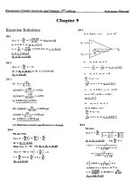
report electronic circuit 1 audio amplifier
Bạn đang xem bản rút gọn của tài liệu. Xem và tải ngay bản đầy đủ của tài liệu tại đây (4.68 MB, 22 trang )
<span class="text_page_counter">Trang 1</span><div class="page_container" data-page="1">
<b>Instructor: PhD Nguyen Vu Thang Student’s name: Pham Viet Hoang </b>
<b>Student’s ID: 20182951</b>
<b>AUDIO AMPLIFIER REPORT:</b>
- ---
<b><small>--SCHOOL OF ELECTRONIC AND TELECOMUNICATION</small></b>
</div><span class="text_page_counter">Trang 2</span><div class="page_container" data-page="2">4.2. Stage 1: Voltage amplifier...7
4.3. Stage 2: Current amplifier...10
4.4. Stage 3: Power amplifier...15
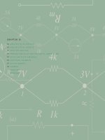
</div><span class="text_page_counter">Trang 3</span><div class="page_container" data-page="3"><b>List of figures:</b>
Figure 1: Block
Figure 2: Audio- amplifying circuit sketch………7
Figure 3: Voltage- amplifying circuit sketch………8
Figure 4: Current- amplifying circuit sketch………9
Figure 5: Power- amplifying circuit sketch………..10
Figure 6: Circuit simulation on the Proteus software………11
Figure 7: Simulating result on Oscilloscope……….11
</div><span class="text_page_counter">Trang 4</span><div class="page_container" data-page="4"><b>1. Introduction</b>
In term 2021.1,I learn about amplifiers and transistors, and now,I design the audio amplifier circuit using BJT for more understanding about its operation and its application.
<b>Non-functional requirements: </b>
Simple, easy to use. Easy to fix. Low cost. • Compact size
2.2. Description
The audio power amplifier, also known as the audio amplifier, is a type of electronic amplifier that amplifies low-power audio impulses to a level sufficient for driving loudspeakers (the frequencies of low-power signals are always between20Hz and 20KHz, which is the range of human hearing). A three-stage circuit mustbe designed to build a full circuit for the audio power amplifier.
2.3. Parameters
Power supply: 15VDC.
</div><span class="text_page_counter">Trang 5</span><div class="page_container" data-page="5">Input signal: 100mV AC (The signal is supplied through the audio jack from our computer or smartphone).
Efficiency: Frequency response: Frequency response is the term used to describe the range of tones that a stereo system can reproduce. The range of frequency response should be wide enough (20Hz to 20 KHz). The frequency response should be flat (linear).
Amplifier gain: Combination of the pre-amplifier’s gain and the amplifier.
<b>power-3. Block diagram</b>
Our product is divided into 6 main parts: AC input signal, Power supply, Voltage amplifier, Current amplifier, Power amplifier and Speaker or Load.
<small>Figure 1: Block </small>
</div><span class="text_page_counter">Trang 6</span><div class="page_container" data-page="6"><b>4. Block designing</b>
4.1. Circuit sketch
</div><span class="text_page_counter">Trang 7</span><div class="page_container" data-page="7">We use:
• The NPN transistor, BC547 to amplify the small input signal because it is used asa small signal transistor for VHF (very high frequency) amplifier.
• TIP41C, TIP42C to amplify the power of signal because they are power BJT.
4.2. Stage 1: Voltage amplifier
We employ the Common-Emitter voltage-divider bias setup in the voltage amplifier circuit. The voltage-divider bias setup is less affected by temperature changes, which is why it is more stable than other biasing systems. The voltage gain is increased by using the bypass capacitor.
<small>Figure 2: Audio- amplifying </small>
</div><span class="text_page_counter">Trang 8</span><div class="page_container" data-page="8"><b>DC Mode:</b>
<small>Figure 3: Voltage- amplifying </small>
</div><span class="text_page_counter">Trang 9</span><div class="page_container" data-page="9">- Based on the data sheet of BC547, choose:+ The working point of Q is: = 6V ; = 12.5mA+ = 250
- Apply Kirchoff’s voltage law: = . + . + . +
+ + = = = 720
Since + is the emitter voltage at Q point.Choose: + = = 120 = 720 – 120 = 600 In reality: Choose = = 300 - = = 2.08
- Assume = 45
= 45 => = 45 = 11.25
= 11
- + = 120 => = 109 =110
= 91.2 = 91
- Since << => The circuit is stable. << (+ ) = 250 x 120 = 30000 = = 3k
- Apply Kirchoff’s voltage law: . = . + + +
= x + 0.7V + 1.5V = 16.34k
= 16k ; = 330
</div><span class="text_page_counter">Trang 10</span><div class="page_container" data-page="10"><b>AC Mode:</b>
- = // // .( + ) = 16.34k // // 250x(2.08 + 11 ) = 1427.87
- =
= 600 - = 5.6
Choose = 100 - Similarly, choose = 100 Current of the output signal:- = =
= 0.07 mA-
=
15992
4.3. Stage 2: Current amplifier
I choose emitter – follower Darlington connection configuration to amplifier the current. Stage 1 does not amplify the current so much. At this configuration, the voltage gain is always approximately 1. I want to use this circuit to amplifier the small current with high gain to increase the Power.
</div><span class="text_page_counter">Trang 11</span><div class="page_container" data-page="11">= = 0.07 mA
- Stage 2 need to amplify to the value of Current gain of stage 2 is:
= = = 640
- does not amplify the voltage, so assume that = 1 = .
= = 38.53 k Choose = 39 k
<b><small>DC MODE:</small></b>
<small>Figure 4: Current- amplifying </small>
</div><span class="text_page_counter">Trang 12</span><div class="page_container" data-page="12">Because the output current of this stage will cause important effect on stage 3 (namely heat effect on T4 & T5), so based on the datasheet of TIP41, I choose the working point of T3 is ( = 6V, = 0.25A). At that point = 55.
= - = 15 – 6 = 9V
</div><span class="text_page_counter">Trang 13</span><div class="page_container" data-page="13">- From the operation point of , assume that = 0.73V = 0.25 A
= = = 4.55 mA = = 4.55 mA
</div><span class="text_page_counter">Trang 14</span><div class="page_container" data-page="14">- With = 4.55 mA, based on the datasheet of BC547, choose = 110.- Similarly, assume = 0.7V
= = = 41 -
= . + + + = = = 111.46 k = 112 k = =
= 36
<b>AC MODE:</b>
= = = 0.1
= // (// ) = 112 k // [110 x 55 x (36 // 60.2 )] = 61.5 k ( > = 39 k )
= 0.1 = = 0.13 Choose = 100
4.4. Stage 3: Power amplifier
The output stage of a Class AB amplifier combines the benefits of both a Class A and a Class B amplifier while reducing the drawbacks of each, such as low efficiency and distortion. It outperforms class A and has less distortion than class B. I employ a pair of normal forward biased diodes within the amplifier's biasing configuration to correct for any temperature-related change in the base-emitter voltage (VBE), as illustrated below.
</div><span class="text_page_counter">Trang 15</span><div class="page_container" data-page="15">- The output device is an 4 – 3W speaker.
- To avoid damage the equipment, we have: = 4 , = = 2.5W
= = V
= = 3.16V x 4.5 VThe input voltage is 100mV
The maximum voltage gain of the system is: = =
= 45
- avoid signal distortion, choose 2 = 2 x 4.5 = 9V
<small>Figure 5: Power- amplifying </small>
</div><span class="text_page_counter">Trang 16</span><div class="page_container" data-page="16">= 15V = = = 1.12 A
- Based on the datasheet of TIP41 and TIP 42, assume that = = 50 = = = = 22.4mA
Apply Kirchoff’s voltage law: = + + +
+ = - - = 15V – 0.7V – 0.7V = 13.6V= = = 6.8V
= = = = 303.57 = = 300 = 1.99
Choose = 2.2 mF = = = 0.023
Consider one half of this stage:
= // .( + ) = 300 // 50x(0.023 + 4 = 120.41 = = 60.2
= 0.023
Input current for this stage to get the maximum power of the speaker: = . = 1. = 30.1
= = = = 37.2 mA = + = 22.4mA + 22.4mA
</div><span class="text_page_counter">Trang 17</span><div class="page_container" data-page="17">= 44.8 mA = = = 66
<small>Figure 6: Circuit- Simulation on the </small>
</div><span class="text_page_counter">Trang 18</span><div class="page_container" data-page="18">5.2. Simulating result
</div><span class="text_page_counter">Trang 19</span><div class="page_container" data-page="19"><b>6.Testing with breadboard</b>
</div><span class="text_page_counter">Trang 21</span><div class="page_container" data-page="21"><b>7.Layout PCB circuit</b>
</div><span class="text_page_counter">Trang 22</span><div class="page_container" data-page="22"><small>On the breadboard, the output sound is audible, however TIP41 and TIP42 are extremely hot.I learned how to construct electronic circuits and run simulations as a result of this assignment. I may have made a mistake during the procedure, and I am hoping that the teacher can assist me in correcting it. Thank you so much for everything.</small>
</div>