design and optimization of approximate adder using advanced cmos technology
Bạn đang xem bản rút gọn của tài liệu. Xem và tải ngay bản đầy đủ của tài liệu tại đây (13.43 MB, 85 trang )
<span class="text_page_counter">Trang 1</span><div class="page_container" data-page="1">
MINISTRY OF EDUCATION AND TRAINING
<b>HO CHI MINH CITY UNIVERSITY OF TECHNOLOGY AND EDUCATION FACULTY FOR HIGH QUALITY TRAINING </b>
<b> </b>
<b>GRADUATION PROJECT </b>
<b>ELECTRONICS AND COMMUNICATIONS</b>
<b>DESIGN AND OPTIMIZATION OF APPROXIMATE ADDER USING ADVANCED CMOS TECHNOLOGY</b>
<b>LECTURER: PhD. PHAM VAN KHOA</b>
<b>STUDENT: LUONG NGOC PHUONG QUYNH NGUYEN PHUC HUNG</b>
<b>Ho Chi Minh City, January 2024</b>
<small>S K L 0 1 2 4 9 7 </small>
</div><span class="text_page_counter">Trang 2</span><div class="page_container" data-page="2"><b>LUONG NGOC PHUONG QUYNH19161050</b>
<b>NGUYEN PHUC HUNG19161013</b>
<b>Major:<sup>Electronics and Communications Engineering</sup><sub>Technology</sub></b>
Ho Chi Minh City, January 2024
<b>DESIGN AND OPTIMIZATION OF APPROXIMATEADDER USING ADVANCED CMOS TECHNOLOGY</b>
</div><span class="text_page_counter">Trang 3</span><div class="page_container" data-page="3">THE SOCIALIST REPUBLIC OF VIETNAM
<b>Independence – Freedom– Happiness</b>
<i>---Ho Chi Minh City, January , 2024</i>
<b>GRADUATION PROJECT ASSIGNMENT</b>
Student name: Luong Ngoc Phuong Quynh
_________________________ <sup>Student ID: 19161050</sup>Student name: Nguyen Phuc Hung
__________________________ <sup>Student ID: 19161013</sup>Major: Electronics and Communications
<b>CHAIR OF THE PROGRAM</b>
<i>(Sign with full name)</i>
</div><span class="text_page_counter">Trang 4</span><div class="page_container" data-page="4"><small>IVTHE SOCIALIST REPUBLIC OF VIETNAM</small>
<b><small>Independence – Freedom– Happiness</small></b>
<i><small>---Ho Chi Minh City, January , 2024</small></i>
<b>ADVISOR’S EVALUATION SHEET</b>
Student name: LuongNgoc Phuong Quynh Student ID: 19161050Student name: Nguyen Phuc Hung Student ID: 19161013Major: Electronics and Communications Engineering Technology
Project title: Design and optimization of approximate adder using advanced CMOStechnology
Advisor: Ph.D Pham Van Khoa
1. Content of the project:
Discovery to high-performance adders and optimize it into approximate adders,simulating based on 90nm cmos technology
</div><span class="text_page_counter">Trang 5</span><div class="page_container" data-page="5"><small>THE SOCIALIST REPUBLIC OF VIETNAM</small>
<b><small>Independence – Freedom– Happiness</small></b>
<i><small>---Ho Chi Minh City, January , 2024</small></i>
<b>PRE-DEFENSE EVALUATION SHEET</b>
Student name: LuongNgoc Phuong Quynh Student ID: 19161050Student name: Nguyen Phuc Hung Student ID: 19161013Major: Electronics and Communications Engineering Technology
Project title: Design and optimization of approximate adder using advanced CMOStechnology
Name of Reviewer: Ph.D Pham Van Khoa
1. Content and workload of the project
Discovery to high-performance adders and optimize it into approximate adders,simulating based on 90nm cmos technology
<i>(Sign with full name)</i>
</div><span class="text_page_counter">Trang 6</span><div class="page_container" data-page="6"><small>VITHE SOCIALIST REPUBLIC OF VIETNAM</small>
<b>Independence – Freedom– Happiness</b>
<i><small>---Ho Chi Minh City, January , 2024</small></i>
<b>EVALUATION SHEET OF DEFENSE COMMITTEE MEMBER</b>
Student name: LuongNgoc Phuong Quynh Student ID: 19161050Student name: Nguyen Phuc Hung Student ID: 19161013Major: Electronics and Communications Engineering Technology
Project title: Design and optimization of approximate adder using advanced CMOStechnology
Name of Defense Committee Member: Ph.D Pham Van Khoa
1. Content and workload of the project
Discovery to high-performance adders and optimize it into approximate adders,simulating based on 90nm cmos technology
<b>COMMITTEE MEMBER</b>
<i>(Sign with full name)</i>
</div><span class="text_page_counter">Trang 7</span><div class="page_container" data-page="7"><b>THANK YOU</b>
During my time studying at Ho Chi Minh City University of Technical Education, Iwould like to express my sincere thanks to the School Board of Directors and the teachersfor creating the best learning conditions and environment for me so that I can concentrateon studying and researching.
Furthermore, I want to convey my sincere thanks to the professors and instructors atthe Faculty of High-Quality Education for their commitment to teaching and for inspiringme to study more about every topic so that I may arm myself with the finest toolspossible for the future.
I want to express my gratitude to Ph.D. Pham Van Khoa, my instructor, in particular,for his passionate guidance and advice. Throughout the composition of this researchpaper, he supported me, offered advice, and assisted with editing so that I could finish mygraduation thesis as effectively as feasible.
However, my research cannot be perfect owing to restricted conditions and expertise.I so eagerly await your input so that I may improve my writing and add to my expertisefor next research projects. These are insightful remarks that will aid me in the future inrefining both my thesis and my expertise.
Finally, I would want to thank you very much again and wish you continued health,happiness, and professional success.
</div><span class="text_page_counter">Trang 8</span><div class="page_container" data-page="8">In order to handle an ever-increasing amount of data, computer systems' overallenergy consumption is still rising alarmingly quickly, despite advancements insemiconductor technology and the development of energy-efficient design strategies. Inparticular, computer systems are being utilized more and more to handle vast amounts ofdata from diverse sources and interact with the real environment as they become moreand more commonplace.
In addition, we anticipate that they will exhibit realistic human interfaces and contextawareness. As a result, a vast array of applications—known as Recognition, Mining, andSynthesis, or RMS—have surfaced, and they now consume a substantial amount ofcomputational resources in a variety of computing contexts, from large-scale data centersto mobile and Internet of Things (IoT) devices. In order to handle the increasing amountof data, it is imperative to significantly increase the energy efficiency for these newworkloads. Thankfully, these applications typically include an inherent error-resiliencecharacteristic. They handle redundant and noisy data from unconventional input sources,such different kinds of sensors (inexact inputs), and the corresponding methods arefrequently stochastic (e.g., iterative algorithms). Furthermore, these applications typicallydo not need to calculate a singular or ideal numerical result (i.e., "acceptable" outputsrather than exact ones).
Ensuring error-free calculations becomes more and more energy-intensive assemiconductor technology moves closer to the nanoscale range. This is because atadvanced technology nodes with low supply voltage and constantly rising integrationdensity, circuits are more susceptible to errors and fluctuations in parameters. Forvariation tolerance and error correction, guardbands and redundancies are needed atdifferent levels of the design hierarchy in conventional fault-free computing, whichresults in a large energy overhead.
Inspired by the aforementioned difficulties, approximation computing has emerged asa highly promising alternative that has gained considerable support in both academia andindustry. Aiming for large energy-efficiency advantages, approximation computingintentionally inserts "acceptable errors" into the computing process by loosening thenumerical equivalency between the design and implementation of error-tolerantapplications.
</div><span class="text_page_counter">Trang 9</span><div class="page_container" data-page="9"><b>TABLE OF CONTENTS</b>
GRADUATION PROJECT ASSIGNMENT...IIIADVISOR’S EVALUATION SHEET... IVPRE-DEFENSE EVALUATION SHEET ...VEVALUATION SHEET OF DEFENSE COMMITTEE MEMBER... VITHANK YOU...VIISUMMARY... VIIITABLE OF CONTENTS... IXTABLE OF FIGURE...XITABLE OF TABLE...XIV
Chapter 2 : THEORETICAL BASIS ...4
2.1 The Full Adder Circuit... 4
2.1.1 The CLRCL (Complementary & Level Restoring Carry Logic) Full Adder 72.1.2 High-gate-count full adder designs (TG-CMOS, TFA, 14T, 16T)... 9
2.1.3 The 10T Full Adder Design... 13
2.2 The XOR/XNOR circuits... 14
2.2.1 The 8T XOR-XNOR... 15
2.2.2 The 10T XOR-XNOR circuit...15
2.2.3 The 4-transistor XOR/XNOR circuits... 17
2.3 Approximate XOR/XNOR-based Adders design... 18
2.3.1 Approximate Adders... 18
2.3.2 Approximate Circuits And Their Implementation...25
2.4 Process Design Kit...29
</div><span class="text_page_counter">Trang 10</span><div class="page_container" data-page="10">2.4.1 Generic Process Design Kit (GPDK) 90 nm technology (gpdk90)... 30
2.4.2 Generic Process Design Kit (GPDK) 180 nm technology (gpdk180)... 31
Chapter 3 : CONSTRUCT THE IDEAL APPROXIMATE ADDER ...32
3.1 Optimal Design Quality...32
3.1.1 Optimization of XNOR... 32
3.1.2 Optimization of full adder:...38
3.2 Optimization of Adder design methods... 50
3.2.1 Optimization of Adder design methods: Low-part OR Adder (LOA)...50
3.2.2 Optimization of Adder design methods: Hardware Efficient ApproximateAdder (HEAA)... 51
Chapter 4 : RESULTS OF SIMULATION, COMPARISON, ANALYSIS ANDSYNTHESIS... 53
4.1 Results of simulation by Cadence... 53
4.1.1 A comparison delay of each full adder in 90, 180nm: 10T adder (90nmand 180nm) ... 53
4.1.2 A comparison power of each full adder in 90, 180nm 10T adder (90nmand 180nm) ... 55
4.2 Analysis of result... 56
4.2.1 A software tool for automatic generation of approximate arithmetic circuits564.2.3 Relation of the computing approximate_LOA (Lower-Part Or AdderDesign), 10T, XOR/XNOR ...60
4.2.2 Relation of the computing approximate_HEAA (Hardware EfficientApproximate Adder Design), 10T, XOR/XNOR... 63
Chapter 5 : CONCLUSION AND DEVELOPMENT DIRECTION... 65
5.1 Conclusion... 65
5.2 Development Direction ...65
REFERENCE...67
</div><span class="text_page_counter">Trang 11</span><div class="page_container" data-page="11"><b>TABLE OF FIGURE</b>
Figure 2- 1 The symbol of full adder...5
Figure 2- 2 Block Diagram of basic full adder circuit... 7
Figure 2- 3 Logic circuit diagram of a 2-bit full adder... 7
Figure 2- 4 Logic block diagram of the CLRCL full adder... 8
Figure 2- 5 MOS circuit schematic design of the CLRCL full adder...9
Figure 2- 6 The Full Adder circuit using transmission gates ...10
Figure 2- 7 The TFA (Transmission Function Adder) full adder... 12
Figure 2- 8 The 14T full adder design ...12
Figure 2- 9 The 16T full adder design ...13
Figure 2- 10 The 10T full adder design...14
Figure 2- 11 The 8-transistor XOR/XNOR circuits... 15
Figure 2- 12 10-transistor XOR/XNOR circuits... 16
Figure 2- 13 The 4-transistor XOR/XNOR circuits... 18
Figure 2- 14 Accurate XOR/XNOR-based 10T Full-Adders...19
Figure 2- 15 Conventional 10T full adder designs: The New Static Energy-Recovery Full(SERF) Adder... 20
Figure 2- 16 Architecture of lower-part OR adder (LOA) ...21
Figure 2- 17 Operation of proposed adder...23
Figure 2- 18 Operations of proposed error reduction when An−k−1 and Bn−k−1 areidentical...24
Figure 2- 19 Operations of proposed error reduction when An−k−1 and Bn−k−1 areexclusive...24
Figure 2- 20 Approximate Adder (HEAA) Design... 25
Figure 2- 21 Approximate XOR-based Adder 1 (AXA1)...25
Figure 2- 22 Approximate XNOR-based Adder 2 (AXA2)...26
Figure 2- 23 Approximate XNOR-based Adder 3 (AXA3)...28
Figure 2- 24 Process Design Kit (PDK) provides necessary information for the circuitdesign... 30
Figure 3- 1 Schematic of 4T XOR-XNOR circuit... 32
</div><span class="text_page_counter">Trang 12</span><div class="page_container" data-page="12">Figure 3- 2 Waveforms of the outputs of 4T XOR/XNOR circuit... 33
Figure 3- 3 TPHL and TPLH of 4T XNOR circuit... 33
Figure 3- 4 The average power of 4T XNOR...34
Figure 3- 5 Schematic of 8T XNOR...34
Figure 3- 6 Waveforms of the outputs of 8T XOR/XNOR circuit... 35
Figure 3- 7 TPHL and TPLH of 8T XNOR...35
Figure 3- 8 The average power of 8T XNOR...36
Figure 3- 9 Schematic of 10T XOR/XNOR circuit...36
Figure 3- 10 Waveforms of the outputs of 10T XOR/XNOR circuit... 37
Figure 3- 11 TPHL and TPLH of 10T XNOR ...37
Figure 3- 12 The average power of 10T XNOR. ...38
Figure 3- 13 Schematic of SERF Full Adder ... 39
Figure 3- 14 Waveforms of the outputs of SERF Full Adder circuit...39
Figure 3- 15 TPHL and TPLH of SERF Full Adder... 40
Figure 3- 16 The average power of SERF...40
Figure 3- 17 Schematic of TFA Full Adder... 41
Figure 3- 18 Waveforms of the outputs of TFA Full Adder circuit...41
Figure 3- 19 TPHL and TPLH of TFA Full Adder... 42
Figure 3- 20 The average power of TFA Full Adder... 42
Figure 3- 21 Schematic of 14T Full Adder...43
Figure 3- 22 Waveforms of the outputs of 14T Full Adder circuit...43
Figure 3- 23 TPHL and TPLH of 14T Full Adder... 44
Figure 3- 24 The average power of 14T Full Adder... 44
Figure 3- 25 Schematic of 16T Full Adder...45
Figure 3- 26 Waveforms of the outputs of 16T Full Adder circuit...45
Figure 3- 27 TPHL and TPLH of 16T Full Adder circuit...46
Figure 3- 28 The average power of 16T Full Adder... 46
Figure 3- 29 Schematic of CLRCL Full Adder...47
Figure 3- 30 Waveforms of the outputs of CLRCL Full Adder circuit... 47
Figure 3- 31 TPHL and TPLH of CLRCL Full Adder...48
</div><span class="text_page_counter">Trang 13</span><div class="page_container" data-page="13">Figure 3- 32 The average power of CLRCL Full Adder...48
Figure 3- 33 Column chart show the average power of Full Adder... 49
Figure 3- 34 Column chart show the delay of Full Adder... 50
Figure 3- 35 1-bit Full Adder ...51
Figure 3- 36 The 6-bit Low-part OR Adder design...51
Figure 3- 37 1-bit Full Adder ...52
Figure 3- 38 The 6-bit Hardware Efficient Approximate Adder design...52
Figure 4- 1 The waveform of delay of SERF... 53
Figure 4- 2 TPHL and TPHL of SERF in 180nm... 54
Figure 4- 3 Column chart show delay of SERF in 90nm and 180nm ...54
Figure 4- 4 The waveform of average power of SERF... 55
Figure 4- 5 The average power of SERF in 90nm...55
Figure 4- 6 Column chart show average power of SERF in 90nm and 180nm. ...56
Figure 4- 7 A software tool for automatic generation of approximate arithmetic circuits 57Figure 4- 8 Flowchart describing the use of the GUI version of Approximator... 58
Figure 4- 9 Display 8-bit approximate adders with a 3-bit inaccurate part usingApproximator GUI: HEAA... 59
Figure 4- 10 Result of AE, MAE, and RMSE for 8-bit approximate adders with a 3-bitinaccurate part using Approximator GUI: HEAA... 60
Figure 4- 11 Design the full adder SERF on Cadence simulation software...61
Figure 4- 12 Design the computing approximate LOA on Cadence simulation software 61Figure 4- 13 The input values of the adder computing approximate LOA in example1...62
Figure 4- 14 Result of the LOA in example 1... 62
Figure 4- 15 Design the computing approximate HEAA on Cadence simulation software...63
Figure 4- 16 The input values of the adder computing approximate HEAA in example 2....64
Figure 4- 17 Result of the HEAA in example 2... 64
</div><span class="text_page_counter">Trang 14</span><div class="page_container" data-page="14"><b>TABLE OF TABLE</b>
Table 2- 1 The Full Adder Truth...5
Table 2- 2 Logical Expression for Sum...6
Table 2- 3 Logical Expression for Cout... 6
Table 2- 4 XOR and XNOR gate function... 15
Table 2- 5 Output voltage levels of 4T XOR/XNOR circuit... 18
Table 2- 6 Truth Table for precise adder and approximate adder for 1-bit addition...22
Table 2- 7 Truth Table of AXA1 Full Adder... 26
Table 2- 8 Truth Table of AXA2 Full Adder... 27
Table 2- 9 Truth Table of AXA3 Full Adder. ... 28
Table 3- 1 The compare of 4T, 8T, 10T about average power and delay circuits...38
Table 3- 2 The average power of Full Adder in 90nm...49
Table 3- 3 The delay of Full Adder in 90nm...50
Table 4- 1 Delay of SERF in 90nm and 180nm... 54
Table 4- 2 Average power of SERF in 90nm and 180nm...56
Table 4- 3 Specification of Verilog code generator constraints in Approximator... 58
Table 4- 4 Contraints associated with the error analysis of approximate arithmetic circuitsin Approximator...59
</div><span class="text_page_counter">Trang 15</span><div class="page_container" data-page="15"><b>LIST OF ACRONYMS</b>
LOA: Lower-part Or Adder Design
HEAA: Hardware Efficient Approximate Adder DesignCMOS: Complementary Metal-Oxide-SemiconductorASIC: Application-Specific Integrated Circuit
PDA: Personal Digital AssistantsVLSI: Very-large-scale integrationTGA: Transmission Gate Adder
CPL: Complementary Pass-Transistor Logic
CLRCL: Complementary and Level Restoring Carry LogicSERF: Static Energy Recovery Full adder
RC: Resistor–CapacitorLSB: Least Significant BitMSB: Most Significant BitPDK: Process Design Kit
PIC: Photonic Integrated CircuitsLVS: Layout Versus SchematicLPE: Layout Parasitic ExtractionDRC: Design Rule Checking
GPDK: Generic Process Design KitEDA: Electronic Design AutomationHDL: Hardware Description LanguageFPGA: Field-Programmable Gate Array
</div><span class="text_page_counter">Trang 16</span><div class="page_container" data-page="16"><b>Chapter 1 : INTRODUCTION</b>
The basic idea behind approximate XOR/XNOR based adders is explained in the firstchapter along with the project description, research object, methods, and goals.Furthermore, the report's overall layout is presented below.
<b>1.1 Overview</b>
A significant turning point in the development of contemporary industry andcommerce was the creation of the complementary metal oxide semiconductor (CMOS)integrated circuit. Because of its affordability, simplicity of integration, and performance,it has brought about revolutionary developments in computing. Power efficiency hasgrown to be a top priority for VLSI designers in recent years. The development ofembedded systems, portable electronics, audio- and video-based systems, includingdigital signal processing (DSP) technologies, is one of the major elements contributing tothis trend. These computationally demanding systems must perform their complicatedfunctions with the least amount of power usage while preserving dependability,increasing throughput, and reducing expenses.
Approximate computing has recently emerged as a promising approach toenergy-efficient design of digital systems. Approximate computing relies on the ability ofmany systems and applications to tolerate some loss of quality or optimality in thecomputed result. By relaxing the need for fully precise or completely deterministicoperations, approximate computing techniques allow substantially improved energyefficiency. This resreach reviews recent progress in the area, including design ofapproximate arithmetic blocks, pertinent error and quality measures, and algorithm-leveltechniques for approximate computing.
<b>1.2 Objective</b>
The topic "Design of approximate adder based on limited hardware resources"provides solutions to optimize the design of approximate adder, an important element inmany digital signal processing applications. Approximation adders are used to calculatethe product of two binary numbers, a fundamental calculation in many image processingapplications such as error tolerant image processing, sharpening approaches.
The goal of the project is to design a set of approximately optimal adders in terms ofsize, power and processing speed on a limited hardware resource platform. The solutionwill focus on reducing transistor count and power consumption, improving performance,and increasing processing speed.
These solutions include using optimal adder architecture, optimizing design size, andoptimizing voltage and frequency collapsing expressions to optimize mathematicaloperations.
<b>1.3 Research methods</b>
</div><span class="text_page_counter">Trang 17</span><div class="page_container" data-page="17">Effectively demonstrate the best operating threshold of circuit designs to match thedelay and energy of the circuit based on the optimization of the subcircuits.
Learn the appropriate operating threshold parameters for each basic logic gate, thenapply calculations, compare the results of calculations and select the most suitableparameters.
Learn the principles based on theory and then experiment on Cadence simulationsoftware.
Experimental method:
<small></small> Design subcircuits based on theory, and synthesize the designs.
<small></small> Run simulations using different measurement technology scenarios (90nm and180nm), then select appropriate results and perform performance evaluation based onaccuracy criteria , resource usage, energy consumption and propagation delay threshold.
<b>1.4 Scope</b>
The research object of the project is approximate adders based on exact adders andXOR/XNOR sets. To optimize the design of approximate adders, the project offerssolutions such as using optimal adder architecture, optimizing design size and optimizingvoltage and frequency. However, to apply these solutions, it is necessary to re-design andsimulate the operation of Full Adder and XOR/XNOR sets in different designs such asFull Adder (10T, 14T, 16T,..) ; XOR/XNOR (4T, 8T, 10T).
With conventional adder designs, it is also possible to redesign and reimagine theiroperation to optimize the design of the full adder. However, optimization solutions mayvary depending on the type of full adder and its intended use.
Therefore, to optimize the design of full adders and XOR/XNOR, it is necessary toconduct detailed research and analysis on the structure, operation and requirements ofeach type of full adders and XOR/XNOR, and then Offer appropriate optimizationsolutions.
Because of limited research time, we only learn and analyze two approximate adders:Lower-part Or Adder Design (LOA) and Hardware Efficient Approximate Adder Design(HEAA).
<b>1.5 Research contents</b>
The research topic includes pages, tables, 67 figures and charts. In addition to theintroduction and conclusion, list of acronyms, list of tables and charts, list of referencesand appendices, the topic is structured into 5 sections as follows:
Chapter 1: Survey methods of performing cumulative multiplication, through whichto find optimal methods, thereby building a system and setting tasks and goals for theproject.
</div><span class="text_page_counter">Trang 18</span><div class="page_container" data-page="18"><small>3</small>Chapter 2: Presents the theory and structure of full adders and XOR/XNOR, theirapplications in performing approximate calculations.
Chapter 3: Optimize designs, select optimal methods, and design scalability.
Chapter 4: Conduct simulations, compare and contrast designs, and demonstrate theoptimization of the newly proposed design.
Chapter 5: Conclusions drawn from optimal design, setting out developmentdirections for design.
</div><span class="text_page_counter">Trang 19</span><div class="page_container" data-page="19"><b>Chapter 2 : THEORETICAL BASIS2.1 The Full Adder Circuit</b>
The growing number of battery-powered portable devices like as laptops, personaldigital assistants (PDAs), and mobile phones necessitates the use of VLSI and ultralarge-scale integration architectures with better power delay characteristics. Since fulladders are among the most fundamental building blocks of all the circuit applicationsoutlined above, researchers have continued to work heavily on them throughout the years.Various forms of logic were examined, each with advantages and drawbacks, in order tobuild 1-bit complete adder cells. The designs that have been revealed thus far may belargely divided into two groups: 1) dynamic style and 2) static style. In comparison to itsdynamic version, static full adders often consume less power, are simpler, and are moredependable. However, they also typically require a bigger on-chip space.
Certain logic styles often prioritize some aspects of performance over others. Themost significant logic design types in the conventional arena are transmission gate fulladder (TGA), dynamic CMOS logic, complementary pass-transistor logic (CPL), andstandard static complementary metal-oxide-semiconductor (CMOS). The other adderdesigns utilize a hybrid-logic design style, which combines many logic styles. The totalperformance of the complete adder is enhanced by these designs, which take use of thecharacteristics of various logic types.
In such a full adder circuit, the pass transistor logic module used just ten transistors tocreate the XOR and XNOR functions concurrently. These functions were then used in theCMOS module to produce full-swing outputs of the full adder, although at the expense ofa higher transistor count and slower speed. Even while hybrid logic adders havepromising performance, most of them have weak driving capabilities, and if properlydesigned buffers are not included, their performance significantly deteriorates in thecascaded mode of operation. This work aims to enhance the various performancemetrics of the complete adder, such as power, latency, and transistor count, incomparison to the current ones. Using Cadence Virtuoso tools, the circuit was built inboth 180-nm and 90-nm technology.
A full adder is an electronic circuit that performs the addition of binary numbers. It isa fundamental building block in digital circuits, and it is used in a wide variety ofapplications, including arithmetic logic units (ALUs), counters, and shift registers. Thefull adder is designed to add two one-bit binary numbers, A and B, and a carry-in bit,Cin.
Full Adder is the adder that adds three inputs and produces two outputs. The first twoinputs are A and B and the third input is an input carry as Cin. The output carry isdesignated as Cout and the normal output is designated as S which is Sum. The Cout isalso known as the majority 1’s detector, whose output goes high when more than one
</div><span class="text_page_counter">Trang 20</span><div class="page_container" data-page="20"><small>5</small>input is high. A full adder logic is designed in such a manner that can take eight inputstogether to create a byte-wide adder and cascade the carry bit from one adder to another.we use a full adder because when a carry-in bit is available, another 1-bit adder must beused since a 1-bit half-adder does not take a carry-in bit. A 1-bit full adder adds threeoperands and generates 2-bit results.
Figure 2- 1 The symbol of full adderWhere,
<small></small> Cin : The carry in from the previous stage.
<small></small> Cout : The carry out.
<small></small> Sum : The sum current.
Table 2- 1 The Full Adder Truth
</div><span class="text_page_counter">Trang 21</span><div class="page_container" data-page="21">Minimize the output function using the Karnaugh:
Table 2- 2 Logical Expression for SumAB
</div><span class="text_page_counter">Trang 22</span><div class="page_container" data-page="22"><small>7</small>Figure 2- 2 Block Diagram of basic full adder circuit
Full adder N-bit:
To design an adder with more than 1 bit, we will have to connect many 1-bit adderstogether, by connecting Cin of the previous adders with Cout of the adders.
Figure 2- 3 Logic circuit diagram of a 2-bit full adder.
We can add an adder if we wish to do calculations with additional bits, but this is notadvised since it would increase the propagation delay, which will slow down processingand make signal recovery more difficult.
<b>2.1.1 The CLRCL (Complementary & Level Restoring Carry Logic) Full Adder</b>
CLRCL full adder is a novel full adder design that uses Complementary and LevelRestoring Carry Logic to reduce the circuit complexity and achieve faster cascadeoperation.
</div><span class="text_page_counter">Trang 23</span><div class="page_container" data-page="23">Figure 2- 4 Logic block diagram of the CLRCL full adder
Compared to previous complete adder designs, it has a lower operating voltage,consumes less energy, and contains 10 transistors. In addition to having the lowest energyusage per addition, the CLRCL full adder can withstand lower Vdd operation thancomparable designs.
In order to achieve quicker cascade operation, the complementary and level restoringcarry logic full-adder is a low complexity circuit. In the carry propagate chain, themultiple threshold voltage fit losses problem is resolved by using an appropriate levelrestoring mechanism with an inverter. First, make an effort to refrain from using thestage's degraded output as gate control signals. This is the typical issue with the majorityof 10-transistor full adder designs. In addition to causing repeated threshold voltagelosses, it could prevent the cascaded circuit from operating correctly. Secondly, attemptto remove the transmission of unbuffered carry signals in a pass transistor chain. Thepropagation delay is a quadratic function of the number of cascaded pass transistors,according to the Elmore formula. The latency is unbearable even with a reasonablenumber of cascade lengths. As seen in figure 2-4, a 2-to-1 multiplexer and an inverterimplement the XNOR circuit used in the design. The inverter serves three purposes. It isfirst utilized as a circuit for level restoration in order to counteract output thresholdvoltage loss. MUX 2/3 receives the level restored output after which it generates Carryand Sum signals. There will only be one threshold voltage loss for Carry and Sum whenthey are far from the power supply. Second, the inverter accelerates the carry propagationby acting as a buffer along the carry chain. Thirdly, the inverter supplies thecomplementary signals required for the phase that comes after. Two transistor XORstructures make up the complementary and level restoring carry logic full-adder unit.Inverters are used to produce carry by propagating full swing signals and preventing
</div><span class="text_page_counter">Trang 24</span><div class="page_container" data-page="24"><small>9</small>threshold loss problems. Despite operating in full swing, the carry signal circuit usesmore power. Complementary signals make the XNOR design simpler since they onlyrequire one signal for selection control. Figure 2-5 shows the MOS circuit schematicdesign of a CLRCL complete adder. Ten transistors (5 pMOS and 5 nMOS) are all thatare needed for the complete adder circuit.
Figure 2- 5 MOS circuit schematic design of the CLRCL full adder
<b>2.1.2 High-gate-count full adder designs (TG-CMOS, TFA, 14T, 16T)2.1.2.1 The Transmission Gate Full Adder</b>
The Full Adder circuit using transmission gates is an essential tool in digitalelectronics. This circuit, which builds on the half-adder circuit, gives us the ability to addtwo single-digit binary numbers together and produce a result.
</div><span class="text_page_counter">Trang 25</span><div class="page_container" data-page="25">Figure 2- 6 The Full Adder circuit using transmission gates
A transmission gate is a type of switch that uses transistors, both PMOS and NMOS,connected source to source end and drain to drain. This switch has a Dc characteristicthat is independent of input level and low resistance. The input terminal is connected tothe source ends of NMOS and PMOS, while the output terminal is linked to the drainends of NMOS and PMOS. By connecting an enable "en" signal to one transistor and itscomplemented logic to another using an inverter, both transistors are turned on and offsimultaneously. It transmits by PMOS towards the output while the input is strong 1, andthrough NMOS when the input is strong 0. When the resistance drops and the capacitancerises with an increase in the W/L ratio, the transistor's channel length (L) and channelwidth (W) are modified accordingly.
The NMOS and PMOS transistors, sometimes referred to as pass transistors, are usedin the transmission gate design. The linearized RC network can be used to mimic theworst-case delay of a chain of pass transistors. A resistor is used to represent thetransmission gate's linearized on-resistance, which has been calculated. For everytransistor, the linearized diffusion capacitance is also calculated.
There are several benefits to building a full-adder circuit with a transmission gate.First of all, it does away with the requirement for extra parts like relays or transistors.Second, by shortening the signal route, power consumption is decreased and reactiontimes are improved. Thirdly, it enables more effective design and quicker switchingprocesses.
</div><span class="text_page_counter">Trang 26</span><div class="page_container" data-page="26"><small>11</small>30 transistors are needed for the whole adder construction employing transmissiongate logic. An arithmetic circuit block having three inputs and two outputs (a SUM and aCARRY) is called a complete adder design. N complete adders are needed for every N itaddition. Let's review the steps involved in adding higher binary integers. First, we addthe two numbers' LSBs together. We take the carry, if any, ahead to the next highercolumn bits after recording the total beneath the LSB column. Therefore, if there were acarry from the previous addition, we would have to add three bits when adding the nextneighboring upper column bits. Until the MSB, the circumstances for the additionalupper column bits are also comparable. Therefore, in order to create an adder circuit thatcan add bigger binary values in hardware, a complete adder is required. The addition ofLSBs is the only use for a halfadder. The fundamental component of binary adders is thecomplete adder of the kind mentioned above. Nonetheless, adding one-bit binary valuesis limited to a single complete adder circuit. To create adders that can add binary integerswith more bits, a cascade configuration of these adders can be utilized.
The full-adder circuit with transmission gates has several useful benefits, but it canalso make design easier. A circuit's complexity can be decreased while maintaining theintended functionality by doing away with the requirement for additional components.
<b>2.1.2.2 The TFA (Transmission Function Adder) full adder</b>
One of the two inputs to the XOR circuit in the design must be in complimentaryform. This necessitates the use of an extra inverter, which results in an XOR architecturewith six transistors. There are two alternative short circuit pathways to ground for thiscircuit. This design yields the same delay for sum and carry and derives the load + usingpull up and pull down logic in conjunction with complementary pass logic.Althoughdesigning the function takes twice as many transistors, there is no voltage issue. Theprimary drawback of this logic design is that it requires a greater number of transistorsdue to its lack of driving capacity. Additionally, it produces sum and Cout signals in abalanced manner and has fewer transistors.
The transmission function theory is often the foundation for how a transmissionfunction adder (TFA) operates. For complete adder implementation, it has 16 transistors;as a consequence, power consumption is decreased because fewer transistors are needed.Four transistors make up TFA's crucial data route.
</div><span class="text_page_counter">Trang 27</span><div class="page_container" data-page="27">Figure 2- 7 The TFA (Transmission Function Adder) full adder
<b>2.1.2.3 The 14T full adder design</b>
The main recommendation of this proposed 14-transistor full adder circuit is toreduce the number of transistors in the traditional "Full adder, XOR gate, and TG(Transmission Gate) circuits" based on the pass transistor logic were used. This results inthe design of the 14T full adder circuit as shown in figure 2-8.
Figure 2- 8 The 14T full adder design
By comparing this 14T full adder to earlier full adder attempts, advancements wereachieved that led to improved power consumption and holdup. The 14-transistor fulladder operated wonderfully with significantly less strength loss when equipped with high
</div><span class="text_page_counter">Trang 28</span><div class="page_container" data-page="28"><small>13</small>performance multipliers. However, the adder did not result in a decrease in thresholdpower loss. Furthermore, the 14-Transistor full-adder would use a substantial amount ofpower in comparison to the proposed 28-Transistor and 38-Transistor full-adders. The14-Transistor full adder not only runs at a higher pace but also consumes a considerablysmaller amount of energy—in the microwatt level.
By using the 4-transistor XOR technique, power consumption is decreased and thereare just 14 cell transistors overall. Even though the 14T full adder only uses one inverter,it still has the same output glitch problem. Another drawback is that it adds a static powercomponent to the inverter output. The XOR gate's partial voltage swing when A = B = 0will cause the circuit to drain current from the power source even if it is in a steady state.The N and P transistors will turn on as a result (N is weakly ON). Despite this drawback,this cell is still a great choice for low-power applications because it only contains 14transistors.
<b>2.1.2.4 The 16T Full Adder Design</b>
The 16-transistor 1-bit complete adder shown in the figure 2-9 is built on the4-transistor implementations of the XOR and XNOR operations. Cell latency isdecreased by the transmission gates and pass transistor of the cell. This adder does notrequire inverters or traditional CMOS technology. This eliminates the short-circuit powercomponent of the cell. Finally, the partial voltage swing reduces the power utilized inspecific input combinations (A = B = 0, A = B = 1). The transistors attached to theXOR-XNOR module are switched on and off gradually since the module lacks full-swingoutputs.
Figure 2- 9 The 16T full adder design
<b>2.1.3 The 10T Full Adder Design</b>
</div><span class="text_page_counter">Trang 29</span><div class="page_container" data-page="29">The 10T Adder circuit consists of a one-bit complete adder core with two outputs(sum S and carry out Cout) and three inputs (A, B, and carry in Ci). Five CMOS invertersare coupled to form the adder cell, as seen in figure 2-10. Input A is connected directly tothe first inverter, whereas input B is connected to the second and third inverters. The firstinverter output is connected to the second inverter PMOS drain and the third inverterNMOS drain, whereas the second and third inverter drains are directly connected to inputA. The second inverter output is linked to the fourth inverter input, and input Cinprovides the fifth inverter input. Notably, the power supply VDD is connected to the firstinverter alone. The values of WP1 and WP2 determine the width of PMOS transistors,whereas WN1 and WN2 define the width of NMOS driver transistors used infirst-inverter CMOS inverters.
Figure 2- 10 The 10T full adder design
Cadence simulation demonstrates that the suggested 10T full adder has the lowestpower consumption and the least amount of power-delay product. The unique hybrid fulladder's features, when compared to other previous publications, demonstrate that thedesign has the best power-delay product for carrying out signals. For a large-scalemulti-bit adder, the adder core significantly increases overall performance because of itslittle carryout time delay. less Vt transistor logic gates can function with less propagationdelay and less switching power dissipation when the high Vt transistors are turned offduring active mode of operation. When using standby mode, the low-voltage internalcircuitry is shut down by turning off the high-voltage transistors.
<b>2.2 The XOR/XNOR circuits</b>
The XOR and XNOR gate functions are shown in Table 1 and denoted by ⊕ and ⨀respectively. The logic expression for XOR and XNOR are
A ⨁ B = A'B + AB'A ⨀ B = A'B' + AB
</div><span class="text_page_counter">Trang 30</span><div class="page_container" data-page="30"><small>15</small>Table 2- 4 XOR and XNOR gate function
Figure 2- 11 The 8-transistor XOR/XNOR circuits.
A high output (VDD) is produced when both A and B are the same (0 or 1). This isachieved by both TGs linked to GND turning off and both transmission gates connectedto VDD turning on. The XNOR function is corresponding to this.
One TG linked to VDD turns on and the other goes off when A and B are different.Furthermore, one TG that is linked to GND turns on and the other one shuts off. As aresult, the XOR function is represented as a low output (GND).
<b>2.2.2 The 10T XOR-XNOR circuit</b>
Several XOR-XNOR design strategies have been established in the last several years.There exist two construction methods for XOR-XNOR circuits. The first approach iscreating the XOR circuit first, then obtaining the XNOR output—basically, atransmission gate adder (TGA)—by means of an inverter. The main issue is that incorrectswitching and glitches in the outputs of Modules II (sum circuit) and III (carry circuit)
</div><span class="text_page_counter">Trang 31</span><div class="page_container" data-page="31">arise from the XOR and XNOR outputs not being generated concurrently. To overcomethis shortcoming of the second method, the XOR–XNOR circuit is constructed so that theXOR and XNOR outputs are generated simultaneously. Furthermore, an attempt is madeto minimize the difference in delay between the XOR and XNOR signals.
Radhakrishnan exhibited an XOR-XNOR circuit that uses just six transistors toprovide full swing outputs and has acceptable delay performance for inputs 01 and 10,but a switching delay for inputs 11 and 00. Naseri and Timarchi added four moretransistors—two nMOS and two pMOS—to solve this issue. This design reduces powerconsumption in addition to resolving the delayed response issue.
The suggested XOR-XNOR circuit reduces the total delay and power consumption ofthe XOR-XNOR circuit by replacing the extra transistors and internal inverters at theinput (A-) with fewer of them.
The 10-transistors are used to form the suggested XOR-XNOR circuit, which is basedon the cross-couple construction and CPL as seen in figure 2-12. The proposedXOR-XNOR circuit, which is based on the cross-couple construction and CPL as shownin figure 2-12, is formed by the 10-transistors.
Figure 2- 12 10-transistor XOR/XNOR circuits.
As for the XOR output side, it uses two pMOS (P1 and P2) and three nMOS (N3, N4,and N5) transistors; for the XNOR output side, it uses two nMOS (N1 and N2) and threepMOS (P3, P4, and P5). On the xor side and the xnor side, respectively, five transistorsare used. This circuit generates the xor and nor outputs as well as full output swingsimultaneously.
A full swing output is obtained by connecting PTLs P1 and P2, N4, and N5, inparallel with the feedback transistor at the XOR side, nMOS N3. In contrast, P4 and P5are connected as storer transistors to provide a full swing output, N1 and N2 transistors
</div><span class="text_page_counter">Trang 32</span><div class="page_container" data-page="32"><small>17</small>are connected in parallel as PTL, and P3 is connected as a feedback transistor at theXNOR output side.
When two of the inputs, A and B, are set to 01, transistors P2, N1, and P4 turn on.Taking into account that pMOS is a decent logic 1 and nMOS is a great logic 0. Whiletransistors P2 and N1 pass logic "1" and "0" at the XOR and XNOR outputs, respectively,transistor P4 activates transistor P3 to pass the weak logic "0" at the XNOR output.
Additionally, when inputs A and B equal 10, transistors P1, N2, and N4 turn on.Transistor N3 passes the weak logic "1" at the XOR output when transistor N4 activatesit. The logic "1" and "0" are sent via transistors P1 and N2 to the XOR and XNORoutputs, respectively.
The output swing of AB's "01" and "10" will not be affected by the weak logicoutputs because there are paths available for full swing outputs. Transistors P1, P2, P4,and P5 come on when inputs A and B are set to "00." P1 and P2 pass weak logic "0" atthe XOR output, whereas P5 and P4 pass full logic "1" at the XNOR output and theinternal node X.
Logic "1" at node X activates transistor N3, and a strong logic "0" passed at the XORoutput maximizes its output. Transistors N1, N2, N4, and N5 also become active wheninputs A and B equal "11". The XOR node fully discharges through N4 and N5, and thetransistors N1 and N2 pass weak logic "1," for the XNOR output. Furthermore, transistorP3 is turned on by the logic "0" being transmitted to the internal node X, which enablesthe full logic "1" to be passed at the XNOR output.
<b>2.2.3 The 4-transistor XOR/XNOR circuits</b>
In PTL (pass transistor logic), an XOR/XNOR function may be accomplished withjust 4 transistors, as shown in figure 2-13. While the circuits in (c) and (d) are PTL based,the circuits in (a) and (b) are inverter based. Table 5 compiles the output voltages subjectto various input combinations, assuming both inputs have full voltage swing.
The size of a threshold voltage in inverter-based circuits degrades both the outputhigh and low values under specific input combinations. The condition is improved andonly the output high or output low voltage is worsened in PTL-based circuits. Morevoltage deterioration might happen if the compromised output is utilized to regulate thegate of the next stage in pass transistor logic. On the other hand, poor output quality doesnot always indicate a negative impact on circuit performance. Whether or whether theyresult in further voltage drop in the subsequent step will determine this.
</div><span class="text_page_counter">Trang 33</span><div class="page_container" data-page="33">Figure 2- 13 The 4-transistor XOR/XNOR circuits.Table 2- 5 Output voltage levels of 4T XOR/XNOR circuit
<b>2.3.1.1 Accurate XOR/XNOR-based Adders</b>
The XOR-XNOR module discussed before is included in the suggested 10-Tcomplete adder architecture. The whole adder, which has ten transistors overall, is builton four-transistor (4T) XNOR gates, as seen in figure 2-14. I is an internal signal,whereas X, Y, and Cin are inputs.
</div><span class="text_page_counter">Trang 34</span><div class="page_container" data-page="34"><small>19</small>Figure 2- 14 Accurate XOR/XNOR-based 10T Full-Adders
In order to prevent double threshold voltage loss, there is greater flexibility in thepass transistor types that may be used when implementing sum and carry modules whencomplementary control signals are available. By minimizing the deterioration in outputvoltage swing, the design becomes more sustainable when operating at low Vdd.
The non-full swing pass transistor is created in the complete adder 10T employing arestricted number of transistors thanks to the swing restored transmission gate technology.A voltage supply of less than 1.8V will result in improper operation of the whole adder,the power source accounts for the little delay. The main disadvantage of the 10-transistoradder cell is that it generates significant levels of input capacitance.
The cell does not require inverted inputs and just requires ten transistors. The XNORgate full adder design served as the model for the design. The charge delivered to the loadcapacitance during logic level high in a non-energy recovery device is drained to groundat logic level low. Note that there is no direct path to the ground for the new SERF (StaticEnergy Recovery Full adder) adder. Removing a route to the earth lowers powerconsumption and takes the Psc variable—the product of voltage and Isc—out of theequation for total power. Reapplied to the control gates is the charge held at the loadcapacitance. The energy-recovering full adder is an energy-efficient design because itreapplies the load charge to the control gate and lacks a direct connection to ground. Thelowest transistor count for a full adder implementation is achieved with this innovativedesign.
</div><span class="text_page_counter">Trang 35</span><div class="page_container" data-page="35">Figure 2- 15 Conventional 10T full adder designs: The New Static Energy-Recovery Full(SERF) Adder
Inverter buffered XOR/XNOR designs are used in the design to improve drivingcapabilities for cascaded operations and to mitigate the threshold voltage loss issue. Thebuffering circuit is effectively integrated into the whole adder architecture, resulting in areduced number of transistors.
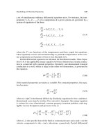
<b>2.3.1.2 Design and Analysis of an Approximate Adder with Hybrid Error Reduction:Lower-Part OR Adder (LOA)</b>
The application of the mentor graphics tool in 90 nm CMOS technology to analyzethe Lower-part OR Adder for 4-bit addition and compare it with the precise adder (RippleCarry Adder).
An equal-segment-based approximation adder splits an n-bit adder into severalequally partitioned smaller k-bit sub-adders that perform partial adds and partial carrygenerations concurrently using a finite number of input bits. It should be noted thatsub-adders can be utilized in ripple carry adders (RCA) and carry lookahead adders(CLA), among other types of classic accurate adders.
An improved low-power high-speed adder for error-tolerant applications and highperformance reliable variable latency carry select addition uses an improved carryspeculation scheme for sub-adders that makes use of 2k and more input bits to generatecarries. This results in a much better computation accuracy than that of the adders. Kahnget al. suggested an accuracy-configurable adder. For approximation arithmetic designs, anaccuracy-configurable adder consists of many 2k-bit sub-adders that overlap k bits toprovide approximate outputs.
</div><span class="text_page_counter">Trang 36</span><div class="page_container" data-page="36"><small>21</small>Figure 2- 16 Architecture of lower-part OR adder (LOA)
In addition, certain least significant bits (LSBs) in a multi-bit adder are added usingapproximately 1-bit complete adders. As seen in Figure 2-16, the Lower-Part OR Adder(LOA) approximates the addition of several LSB inputs by using OR gates. An n-bitadder is split into a (n-k)-bit approximation adder and a k-bit exact adder. The mostsignificant k bit (MSB) inputs and the carry are fed into the exact adder (Cin) to producecorrect outputs for the MSBs. An AND operation of two (n−k−1)th LSB inputs is used toforecast the carry-in signal of the precise adder. Bit-by-bit OR operations are used torealize the (n−k)-bit approximation adder.
To achieve the (n−k)-bit approximation adder for the LSBs, the LOAWA (i.e., LOAwithout AND operation) also employs the OR operation; the primary distinction from theLOA is the removal of the carry prediction technique, which lowers hardware cost at theprice of accuracy. The LOA and the optimized lower-part constant OR adder (OLOCA)are nearly the same. In order to save hardware costs, a few LSB outputs are forced to "1"in the approximation adder portion, which uses the OR function. Put otherwise, the ORoperation generates just a small portion of the higher (n−k) LSB outputs, while theremaining lower bits of the LSB outputs are set to "1."
Both the sub-adder and the full adder are made up of exact and approximate fulladders. The approximate complete architecture of an adder is represented in figure 2-16and consists of an OR gate and an AND gate, where the OR gate generates sum and theAND gate generates carry only in the bit position. Because the carry is not taken intoaccount in the adder's trailing portion, the adder functions roughly but reasonablyefficiently; the approximation is restricted to the adder's trailing bits, and the LSB portionbears the brunt of the approximation mistake because it carries less information. For asingle bit approximation adder, the number of mistakes in sum is '4', whereas in carrythere are '2' errors and the maximum error distance is "2," as Table 2.5 below illustrates.
</div><span class="text_page_counter">Trang 37</span><div class="page_container" data-page="37">Table 2- 6 Truth Table for precise adder and approximate adder for 1-bit addition
<small>(n</small> with the XOR operation. The approximation section of the adder workssimilarly to the LOA, using the OR function to add the lower order input bits of twooperands. This leads to the creation of a half adder for <small>(n-k-1)th</small> LSB inputs andessentially increases the length of accurate addition by one bit. As a consequence, theaccuracy is improved overall as compared to the LOA. Stated differently, the suggestedn-bit adder substitutes the XOR gate at the <small>(n-k-1)th</small> LSB position for the OR gate,therefore always producing valid outputs for bit locations from (n −1) to (n−k−1).Consequently, the suggested adder produces an approximate part output of “01011010”under the input depicted in figure 2-17, whereas the LOA produces an output of“11011010.” The proposed adder's output clearly approaches the correct summation of
</div><span class="text_page_counter">Trang 38</span><div class="page_container" data-page="38"><small>23</small>"01101010" more than the LOA's output does, and the error distance - defined as thedifference between the approximate and correct outputs, as �approximate− �accurate ,respectively, represented by the parameters S<small>approximate</small> and S<small>accurate</small>-for the given inputdrops from "1110000" (112) to "10000" (16).
Figure 2- 17 Operation of proposed adder
When both of the (n−k−2)<small>th</small> input bits are "1" (An−k−2 = 1 and Bn−k−2 = 1), thesuggested approximation adder carries out an error reduction to further reduce the outputerrors. In the absence of such, it makes no effort to reduce errors, as seen by the examplein figure 2-18.
Although the error reduction mechanism is implemented by our adder, in thisinstance, the adder's final outputs are unaffected by this. The way the suggested hybriderror reduction is carried out varies based on the (n−k−1)<small>th</small> inputs. Stated differently, thesuggested adder determines whether of the two error reduction strategies is appropriateby checking the (n−k−1)<small>th</small> output bit. The reduction logic corrects the (n−k−1)<small>th</small> and(n−k−2)<small>th</small>outputs to "1" and "0," respectively, if both inputs are "1" or "0" (S<small>n−k−1:n−k−2</small>="10"). If not, it sets "1" for each and every output from S<small>n−k−3</small>to S<small>0</small>.
After the typical addition described in the operation of the proposed adder, theexample inputs given in figure 2-17 generate the approximate portion output of"01011010"; we label this output the intermediate approximation output. Since both ofthe (n−k−2)<small>th</small> input bits are "1," the adder then verifies the (n−k−1)th output bit. TheXOR operation at the (n−k−1) bit position results in an intermediate approximationoutput S'<small>n−k−1</small>of "0," indicating that the corresponding input bits are equal.
The final adder outputs at the (n−k−1) to (n−k−2) bit locations are "1" and "0,"respectively. S<small>n−k−1:n−k−2</small>= “10,” to put it briefly, is the accurate summation of the outputsat the appropriate locations under the supplied inputs. The error distance is reduced by2<small>n−k−2</small>using this technique.
</div><span class="text_page_counter">Trang 39</span><div class="page_container" data-page="39">Figure 2- 18 Operations of proposed error reduction when An−k−1 and Bn−k−1 areidentical
On the other hand, all the remaining lower order bits are pushed to "1" if theintermediate approximate output S'n−k−1 is "1," as shown in Figure 2-19, yielding anapproximate output of "11111111." A carry is expected to originate in the (n−k−2)th LSBunder the specified input condition and spread to the exact portion via the (n−k−1)thLSB.
However, because the carry prediction is carried out using an AND operation withjust the (n−k−1)th LSB inputs, as can be seen in Figure 2-19, the carry does not reallypropagate to the exact adder (Cin = 0). Because of this outcome, the right total willalways be higher than the addition that was suggested in this particular instance.
Consequently, the approximate output approaches the right summation when all ofthe approximation part's outputs are set to "1." The error distance can be reduced by up to2n−k−2 − 1 using this reduction strategy.
Figure 2- 19 Operations of proposed error reduction when An−k−1 and Bn−k−1 areexclusive
</div><span class="text_page_counter">Trang 40</span><div class="page_container" data-page="40"><b>2.3.1.3 Hardware Efficient Approximate Adder (HEAA) Design</b>
Dividing the precise adder into several smaller components and breaking the carrychain is one of the most popular methods for designing approximation adders. One of themost common approaches to creating approximation adders is to break the carry chainand divide the precise adder into many smaller components. The approximation addersare created by splitting an N-bit dual-operand adder in half. K bits are allocated to theleast significant (inaccurate) sub-adder and (N–K) bits are given to the most significant(accurate) sub-adder. The inaccurate sub-adder in an ASIC technology might be realizedby discrete gates (with or without extra control logic) or even by a second accuratesub-adder that is isolated from the first accurate sub-adder. A carry look ahead or otherhigh-speed adder design might be used to realize the correct sub-adder.
With the exception of suggesting carry lookahead adders for the exact adder portionfor high speed and low power, which is achieved using ASIC technology, the twoOR-based approximation adders are derived from LOA. Our suggested approximationadder, which is a modified version adder designed to mainly enhance the errorcharacteristics without compromising performance, is shown in figure 2-20.
Figure 2- 20 Approximate Adder (HEAA) Design
<b>2.3.2 Approximate Circuits And Their Implementation2.3.2.1 Approximate XOR-based adder 1 (AXA1)</b>
Figure 2- 21 Approximate XOR-based Adder 1 (AXA1).
</div>