deep submicron cmos circuit design simulator in hands
Bạn đang xem bản rút gọn của tài liệu. Xem và tải ngay bản đầy đủ của tài liệu tại đây (14.39 MB, 723 trang )
D
EEP SUBMICRON
CMOS
DESIGN
Contents
1 20/12/03
Deep-submicron
CMOS circuit design
Simulator in hands
Etienne Sicard
Sonia Delmas Bendhia
Version December 2003
This book is under consideration for publication by
Brooks/Cole Publishing Company
3450 South 3650 East Street
Salt Lake City, Utah 84109, USA
www.brookscole.com
(Contact: )
D
EEP SUBMICRON
CMOS
DESIGN
Contents
2 20/12/03
Acknowledgements
We would like our early colleagues Jean-Francois Habigand, Kozo Kinoshita, Antonio Rubio for their support
throughout the development of the Microwind, Dsch tools. The project of writing a book that seemed initially to be
shadowy took form and substance, and led to this present work. We would like to thank Joseph-Georges Ferrante for
having faith in our ability to drive ambitious microelectronics research projects, and having provided us a continuous
support over the last ten years. Productive technical discussions with Jean-Pierre Schoellkopf, Amaury Soubeyran,
Thomas Steinecke, Gert Voland and Jean-Louis Noullet are also gratefully acknowledged.
Special thanks are due to technical contributors to the Dsch and Microwind software (Chen Xi, Jianwen Huang), to our
colleagues at INSA how always supported this work, to numerous professors, students and engineers who patiently
debugged the technical contents of the book and the software, and gave valuable comments and suggestions. Also, we
would like to thank Marie-Agnes Detourbe for having carefully reviewed the manuscript.
Finally we would like to acknowledge our biggest debt to our parents and to our companion for their constant support.
About the authors
ETIENNE SICARD was born in Paris, France, in June 1961. He received a B.S degree in 1984 and a PhD in Electrical
Engineering in 1987 both from the University of Toulouse. He was granted a scholarship from the Japanese Ministry of
Education and stayed 18 months at the University of Osaka, Japan. Previously a professor of electronics in the
department of physics, at the University of Balearic Islands, Spain, E. Sicard is currently professor at the INSA
Electronic Engineering School of Toulouse. His research interests include several aspects of integrated circuit design
including crosstalk fault tolerance, and electromagnetic compatibility of integrated circuits. Etienne is the author of
several educational software in the field of microelectronics and sound processing.
D
EEP SUBMICRON
CMOS
DESIGN
Contents
3 20/12/03
Sonia DELMAS BENDHIA was born in Toulouse, April 1972, She received an engineering diploma in 1995, and the
Ph.D. in Electronic Design from the National Institute of Applied Sciences, Toulouse, France, in 1998. Sonia Bendhia
is currently a senior lecturer in the INSA of Toulouse, Department of Electrical and Computer Engineering. Her
research interests include signal integrity in deep sub-micron CMOS Ics, analog design and electromagnetic
compatibility of systems . Sonia is the author of technical papers concerning signal integrity and EMC.
About Microwind and Dsch
The present book introduces the design and simulation of CMOS integrated circuits, and makes an extensive use of PC
tools Microwind2 and Dsch2. These tools are freeware.
The web link is
In memory…
In memory of John Uyemura
D
EEP SUBMICRON
CMOS
DESIGN
Contents
4 20/12/03
Contents
Chapter
Page
1 Introduction
Technology scale down
Frequency Improvement
Increased layers
Reduced power supply
2 The MOS device
The MOS Logic simulation of the MOS
MOS layout
Vertical aspect of the MOS
Static MOS characteristics
Dynamic MOS behavior
Analog simulation
Mos options
Transmission gate: the perfect switch
Layout considerations
3 MOS modeling
The MOS model 1
The MOS model 3
The model BSIM4
Temperature effects on the MOS
High frequency behavior of the MOS
4 The Inverter
The logic Inverter
The CMOS inverter (Power, supply, frequency)
Layout design (plasma, latchup)
Simulation of the inverter
Views of the process
Buffer
3-state inverter
Analog behavior of the inverter
Ring oscillator
Temperature effects
D
EEP SUBMICRON
CMOS
DESIGN
Contents
5 20/12/03
5 Interconnects
Signal propagation
Capacitance load
Resistance effect
Inductance effect
Buffers
Clock tree
Supply routing
6 Basic Gates
Introduction
From boolean expression to layout
NAND gate (micron, sub-micron)
OR3 gate
XOR
Complex gates
Multiplexors (Mux-demux)
Pulse generator
7 Arithmetics
Data formats: unsigned, signed fixed
Half adder gate
Full adder gate
4-bit adder
Comparator
Multiplier
ALU
Low power arithmetics
8 Latches
RS latch
D-Latch
Edge-trigged latch
Latch optimization (conso, speed, fanout)
Counter
Project: programmable pulse generator
9 FPGA
Goals
Mux for FPGA
Configurable logic block
Look-up table
Interconnection
Programmable Interconnection Points
Propagation delay
10 MEMORIES
The world of Memories
Static RAM memory (4T, 6T)
Decoder (low power)
Dynamic RAM memory
Embedded RAM
Sense ampli
ROM memory
EEPROM memory
FRAM memory
11 Analog Cells
D
EEP SUBMICRON
CMOS
DESIGN
Contents
6 20/12/03
Diode connected MOS
Voltage reference
Current Mirror
Amplifiers (Class)
Voltage regulator
Wide range amplifier
Charge pump
Noise
12 RF Analog Cells
Osc illators
Inductors
Sample & Hold
Mixers
Voltage-controlled Oscillators
PLL project
Power amplifiers
13 Converters
Introduction
Converter parameters
Sample hold
ADC
DAC
14 Input/Output Interfacing
Level shifter
Pad stucture
Input pad (schmidt, protect, buffer)
Output pad (log, analog, multi drive)
Pad ring
Packages
IBIS
LVDS
High performance Ios
15 SOI
Layout improvements
2D aspects
SOI model
Simulation
Issues
16 Future & Conclusion
Appendix A Design rules
Appendix B List of commands Microwind
Appendix C List of commands Dsch
Appendix D Quick Reference Sheet Microwind-Dsch
Appendix E CMOS technology reference Sheet
0.8µm
0.6µm
0.35µm
0.25µm
0.18µm
0.12µm
90nm
Appendix F Answer to exercises
I
NTRODUCTION TO
D
EEP SUBMICRON
CMOS
DESIGN
1. Introduction
7 20/12/03
MULTIPLIERS
Value Name Standard
Notation
10
18
PETA
P
10
15
EXA
E
10
12
TERA
T
10
9
GIGA
G
10
6
MEGA
M
10
3
KILO
K
10
0
-
-
10
-3
MILLI
m
10
-6
MICRO
u
10
-9
NANO
n
10
-12
PICO
p
10
-15
FEMTO
f
10
-18
ATTO
a
10
-21
ZEPTO
z
PHYSICAL CONSTANTS & PARAMETERS
<verify all >
Name Value Description
ε
0
8.85 e
-12
Farad/m
Vacuum dielectric constant
ε
r
SiO
2
3.9 - 4.2
Relative dielectric constant of SiO
2
ε
r
Si 11.8
Relative dielectric constant of silicon
ε
r
ceramic 12
Relative dielectric constant of ceramic
k 1.381e
-23
J/°K
Bolztmann’s constant
q 1.6e
-19
Coulomb Electron charge
µ
n
600 V.cm
-2
Mobility of electrons in silicon
µ
p
270 V.cm
-2
Mobility of holes in silicon
γ
al
36.5 10
6
S/m Aluminum conductivity
γ
si
4x10
-4
S/m Silicon conductivity
n
i
1.02x10
10
cm
-3
Intrinsic carrier concentration in silicon at
300°K
ρ
al
0.0277 Ω.µm Aluminum resistivity
γ
cu
58x10
6
S/m Copper conductivity
ρ
cu
0.0172 Ω.µm Copper resistivity
ρ
tungstène (W)
0.0530 Ω.µm Tungsten resistivity
ρ
or (Ag)
0.0220 Ω.µm Gold resistivity
µ
0
1.257e
-6
H/m Vacuum permeability
T 300°K (27°C) Operating temperature
I
NTRODUCTION TO
D
EEP SUBMICRON
CMOS
DESIGN
1. Introduction
8 20/12/03
Preface
The present book introduces the design and simulation of CMOS integrated circuits, in an attractive way thanks to
user-friendly PC tool Microwind2 given in the companion CD-ROM of this book.
The chapters of this book have been summarized below. Chapter One describes the technology scale down and the
major improvements allowed by deep sub-micron technologies. Chapter Two is dedicated to the presentation of the
single MOS device, with details on simulation at logic and layout levels. The modeling of the MOS devices is
introduced in Chapter Three. Chapter Four presents the CMOS Inverter, the 2D and 3D views, the comparative design
in micron and deep-submicron technologies. Chapter Five deals specifically with interconnects, with information on
the propagation delay and several parasitic effects. Chapter Six deals with the basic logic gates (AND, OR, XOR,
complex gates), Chapter Seven the arithmetic functions (Adder, comparator, multiplier, ALU). The latches and
counters are detailed in Chapter Eight, while Chapter Nine introduces the basic concepts of Field programmable Gate
Arrays.
As for Chapter Ten, static, dynamic, non-volatile and magnetic memories are described. In Chapter Eleven, analog
cells are presented, including voltage references, current mirrors, and the basic architecture of operational amplifiers.
Chapter Twelve is dedicated to radio-frequency analog cells, with details on mixers, voltage-controlled oscillators, fast
phase-lock-loops and power amplifiers. Chapter Thirteen focuses on analog-to-digital and digital to analog converter
principles. The input/output interfacing principles are illustrated in Chapter Fourteen. The last chapter includes an
introduction to silicon-insulator technology, before a prospective and a conclusion.
The detailed explanation of the design rules is in appendix A. The details of all commands are given in appendix B for
the tool Microwind, and in appendix C for the tool Dsch. Appendix D includes a quick reference sheet for Microwind
and Dsch, and Appendix E gives some abstract information about each technology generation, from 0.7µm down to
90nm.
Sonia DELMAS-BENDHIA, Etienne SICARD
Toulouse, Sept 2003
DEEP SUBMICRON CMOS DESIGN 1. The technology scale down
1-1 E. Sicard, S. Delmas-Bendhia 20/12/03
1
Introduction
The evolution of integrated circuit (IC) fabrication techniques is a unique fact in the history of modern industry.
There have been steady improvements in terms of speed, density and cost for more than 30 years. In this chapter,
we present some information illustrating the technology scale down.
1. GENERAL TRENDS
Inside general purpose electronics systems such as personal computers or cellular phones, we may find
numerous integrated circuits (IC), placed together with discrete components on a printed circuit board (PCB), as
shown in figure 1-1. The integrated circuits appearing in this figure have various sizes and complexity. The main
core consists of a microprocessor, considered as the heart of the system, that includes several millions of
transistors on a single chip. The push for smaller size, reduced power supply consumption and enhancement of
services, has resulted in continuous technological advances, with possibility for ever higher integration.
Figure 1-1: Photograph of the internal parts of a cellular phone <Etienne: Or automotive>
DEEP SUBMICRON CMOS DESIGN 1. The technology scale down
1-2 E. Sicard, S. Delmas-Bendhia 20/12/03
Integrated
circuit (Silicon)
Package (FR4)
Balls for
interconnection
Main printed
circuit board
Active part of the IC
Silicon die (350µm
thick, 1cm width)
FR4 package
Metal interconnects
Soldure bumps to
link the IC to the
package (Narrow
pitch)
Soldure bumps to
link the package to
the printed circuit
board (Large pitch)
Printed circuit board
Figure 1-2: Typical structure of an integrated circuit
The integrated circuit consists of a silicon die <Glossary>, with a size usually around 1cmx1cm in the case of
microprocessors and memories. The integrated circuit is mounted on a package (Figure 1-2), which is placed on
a printed circuit board. The active part of the integrated circuit is only a very thin portion of the silicon die. At
the border of the chip, small solder bumps serve as electrical connections between the integrated circuit and the
package. The package itself is a sandwich of metal and insulator materials, that convey the electrical signals to
large solder bumps, which interface with the printed circuit board.
10cm
1cm
1mm
100µm
DEEP SUBMICRON CMOS DESIGN 1. The technology scale down
1-3 E. Sicard, S. Delmas-Bendhia 20/12/03
10 µm
1µm
100nm
10nm
Figure 1-3: Patterns representative of each scale decade from 10cm to 10nm (Courtesy IBM, Fujitsu)
Around eight decades separate the user's equipment (Such as a mobile phone in figure 1-3) and the basic
electrical phenomenon, consisting in the attraction of electrons through an oxide. Inside the electronic
equipment, we may see integrated circuits and passive elements sharing the same printed circuit board (1 cm
scale), wire connections between package and the die (1mm scale), input/output structures of the integrated
circuit (100µm scale), the integrated circuit layout (10µm), a vertical cross-section of the process, revealing a
complex stack of layers and insulators (1µm scale), the active device itself, called MOS transistor (which stands
for Metal oxide semiconductor<glossary>).
Figure 1-4 describes the evolution of the complexity of Intel ® microprocessors in terms of number of devices
on the chip [Intel]. The Pentium IV processor produced in 2003 included about 50,000,000 MOS devices
integrated on a single piece of silicon no larger than 2x2 cm.
82 85 89 92 95 98 01 04
10K
100 K
1 MEG
10 MEG
100 MEG
1 GIGA
N
br of devices
Year
80286
80386
80486
pentium
Pentium III
Pentium II
Pentium 4
16 bits
8086
32 bits
64 bits
Itanium
Figure 1-4: Evolution of microprocessors [Intel]
DEEP SUBMICRON CMOS DESIGN 1. The technology scale down
1-4 E. Sicard, S. Delmas-Bendhia 20/12/03
Since the 1 Kilo-byte (Kb) memory produced by Intel in 1971, semiconductor memories have improved both in
density and performances, with the production of the 256 Mega-bit (Mb) dynamic memories (DRAM) in 2000,
and 1Giga-bit (Gb) memories in 2004 (Figure 1-5). In other words, within around 30 years, the number of
memory cells integrated on a single die has been increased by 1,000,000. An other type of memory chip called
Flash memory has become very popular, due to its capabilities to retain the information without supply voltage
(Non voltaile memories are described in chapter 9). According to the international technology roadmap for
semiconductors [Itrs], the DRAM memory complexity is expected to increase up to 16 Giga-byte (Gb) in 2008.
83 86 89 92 95 98 01 04
100K
1 MEG
10 MEG
100 MEG
1 GIGA
10 GIGA
Memory size (bit)
Year
256K
4M
64M
256M
1G
1M
16M
07
2G
Moore's law:
complexity multiplied
by 2 every 18 months
128M
512M
4G
DRam
Flash
Fig. 1-5: Evolution of Dynamic RAM and Flash semiconductor memories [Itrs][Itoh01]
DEEP SUBMICRON CMOS DESIGN 1. The technology scale down
1-5 E. Sicard, S. Delmas-Bendhia 20/12/03
Figure 1-6: Bird's view of a micro-controller die (Courtesy of Motorola Semiconductors)
The layout aspect of the die of an industrial micro-controller is shown in figure 1-6 [Motorola]. This circuit is
fabricated in several millions of samples for automotive applications. The micro-controller core is the central
process unit (CPU), which uses several types of memory: the Electrically erasable Read-Only Memory
(EEPROM), the FLASH memory (Rapidaly erasable Read-Only Memory) and the RAM memory (Random
Access Memory). Some controllers are also embedded in the same die: the Control Area Network (MSCAN), the
debug interface (MSI), and other functionnal cores (ATD, ETD <Etienne: ask for details to Motorola>).
2. THE DEVICE SCALE DOWN
We consider four main generations of integrated circuit technologies: micron, submicron, deep submicron and
ultra deep submicron technologies., as illustrated in figure 1-7. The sub-micron era started in 1990 with the
0.8µm technology. The deep submicron technology started in 1995 with the introduction of lithography better
than 0.3µm. Ultra deep submicron technology concerns lithography below 0.1µm. In figure 1-7, it is shown that
research has always kept around 5 years ahead of mass production. It can also be seen that the trend towards
smaller dimensions has been accelerated since 1996. In 2007, the lithography is expected to decrease down to
0.07µm. The lithography expressed in µm corresponds to the smallest patterns that can be implemented on the
surface of the integrated circuit.
83 86 89 92 95 98 01 04
0.1
Lithography (µm)
Year
80286
16MHz
80386
33MH
z
486
66MHz
Pentium
120MHz
1.0
0.2
0.3
2.0
0.05
Research
D
eep
s
ubmicron
Industry
Pentium II
300MHz
Pentium III
0.7GHz
S
ubmicron
07
M
icron
Ultra deep
s
ubmicron
Pentium IV
3GHz
Figure 1-7: Evolution of lithography
DEEP SUBMICRON CMOS DESIGN 1. The technology scale down
1-6 E. Sicard, S. Delmas-Bendhia 20/12/03
3. FREQUENCY IMPROVEMENT
Figure 1-8 illustrates the clock frequency increase for high-performance microprocessors and industrial micro-
controllers with the technology scale down. The microprocessor roadmap is based on Intel processors used for
personal computers [Intel], while the micro-controllers roadmap is based on Motorola micro-controllers
[Motorola] used for high performance automotive industry applications. The PC industry requires
microprocessors running at the highest frequencies, which entails very high power consumption (30 Watts for
the Pentium IV generation). The automotive industry requires embedded controllers with more and more
sophisticated on-chip functionalities, larger embedded memories and interfacing protocols. The operating
frequency follows a similar trend to that of PC processors, but with a significant shift.
83 86 89 92 95 98 01 04
10 MHz
100 MHz
1 GHz
Operating frequency
Year
80286
486
Pentium II
Pentium III
Pentium IV
80386
Pentium
07
10 GHz
M
icroprocessors
(Intel)
MPC 555
68HC12
68HC08
68HC16
MPC 765
M
icrocontrolers
(Motorola)
Figure 1-8: Increased operating frequency of microprocessors and micro-controllers
4. LAYERS
The table below lists a set of key parameters, and their evolution with the technology. Worth of interest is the
increased number of metal interconnects, the reduction of the power supply VDD and the reduction of the gate
oxide down to atomic scale values. Notice also the increase of the size of the die and the increasing number of
input/output pads available on a single die.
Lithography Year Metal
layers
Core
supply
(V)
Core Oxide
(nm)
Chip size
(mm)
Input/output
pads
Microwind2
rule file
1.2µm 1986 2 5.0 25 5x5 250 Cmos12.rul
DEEP SUBMICRON CMOS DESIGN 1. The technology scale down
1-7 E. Sicard, S. Delmas-Bendhia 20/12/03
0.7µm 1988 2 5.0 20 7x7 350 Cmos08.rul
0.5µm 1992 3 3.3 12 10x10 600 Cmos06.rul
0.35µm 1994 5 3.3 7 15x15 800 Cmos035.rul
0.25µm 1996 6 2.5 5 17x17 1000 Cmos025.rul
0.18µm 1998 6 1.8 3 20x20 1500 Cmos018.rul
0.12µm 2001 6-8 1.2 2 22x20 1800 Cmos012.rul
90nm 2003 6-10 1.0 1.8 25x20 2000 Cmos90n.rul
65nm 2005 6-12 0.8 1.6 25x20 3000 Cmos70n.rul
Table 1-1: Evolution of key parameters with the technology scale down [ITRS]
The 1.2µm CMOS process features n-channel and p-channel MOS devices with a minimum channel length of
0.8µm. The Microwind tool may be configured in CMOS 1.2µm technology using the command File→ Select
Foundry
, and choosing
cmos12.rul
in the list. Metal interconnects are 2µm wide. The MOS diffusions are
around 1µm deep. The two dimensional aspect of this technology is shown in figure 1-9.
2
nd
level of metal
1
rst
level of metal
Deposited
layers
Diffusion
layers
Low doping P- substrate
(350µm thick)
PMOS device
N
MOS device
1µm
Figure 1-9: Cross-section of the 1.2µm CMOS technology (CMOS.MSK)
The 0.35µm CMOS technology is a five-metal layer process with a minimal MOS device length of 0.35µm. The
MOS device includes lateral drain diffusions, with shallow trench oxide isolations. The Microwind tool may be
configured in CMOS 0.35µm technology using the command File→ Select Foundry, and choosing
"cmos035.rul" in the list. Metal interconnects are less than 1µm wide. The MOS diffusions are less than 0.5µm
deep. The two dimensional aspect of this technology is shown in figure 1-10, using the layout
INV3.MSK
.
DEEP SUBMICRON CMOS DESIGN 1. The technology scale down
1-8 E. Sicard, S. Delmas-Bendhia 20/12/03
3
rd
level of metal
1
rst
level of
metal
Deposited
layers
Diffusion
layers
Trench isolation
N
MOS device
PMOS device
1µm
Figure 1-10: Cross-section of the 0.35µm CMOS technology (INV3.MSK)
The Microwind and Dsch tools are configured by default in a CMOS 0.12µm six-metal layer process with a
minimal MOS device length of 0.12µm. The metal interconnects are very narrow, around 0.2µm, separated by
0.2µm (Figure 1-11). The MOS device appears very small, below the stacked layers of metal sandwiched
between oxides.
6th level of metal
1
rst
level of
metal
Deposited
layers
Diffusion
layers
N
MOS device
PMOS device
1µm
Figure 1-11: 2D View of the 0.12µm process
5. DENSITY
The main consequence of improved lithography is the ability to implement an identical function in an ever
smaller silicon area. Consequently, more functions can be integrated in the same space. Moreover, the number
DEEP SUBMICRON CMOS DESIGN 1. The technology scale down
1-9 E. Sicard, S. Delmas-Bendhia 20/12/03
of metal layers used for interconnects has been continuously increasing in the course of the past ten years. More
layers for routing means a more efficient use of the silicon surface, as for printed circuit boards. Active areas, i.e
MOS devices can be placed closer to each other if many routing layers are provided (Figure 1-12).
The increased density provides two significant improvements: the reduction of the silicon area goes together
with a decrease of parasitic capacitance of junctions and interconnects, thus increasing the switching speed of
cells. Secondly, the shorter dimensions of the device itself speeds up the switching, which leads to further
operating clock improvements.
(a) 1.2µm
600 µm
2
(b) 0.35µm
230 µm
2
(c) 0.12µm
100 µm
2
(d) 90nm
40 µm
2
Figure 1-12: The evolution of the silicon area used to implement a NAND gate, which represents 20% of
logic gates used in application specific integrated circuits
Meanwhile, the silicon wafer, on which the chips are manufactured, has constantly increased in size, with the
technological advances. A larger diameter means more chips fabricated at the same time, but requires ultra-high
cost equipments able to manipulate and process these wafers with an atomic-scale precision. This trend is
illustrated in figure 1-13. The wafer diameter for 0.12µm technology is 8 inches or 20cm (One inch is equal to
2.54 cm). Twelve inches wafers (30cm) have been introduced for the 90nm technology generation. The
thickness of the wafer varies from 300 to 600µm.
DEEP SUBMICRON CMOS DESIGN 1. The technology scale down
1-10 E. Sicard, S. Delmas-Bendhia 20/12/03
300 to 600 µm
thickness
8 inches (20cm)
(0.18µm, 0.12µm)
6 inches (15.2 cm)
(0.35µm, 0.25µm)
5 inches wafer (12.7 cm)
used for 0.6µm, 0.5µm
technologies
12 inches (30.5cm)
(90nm, 65nm)
Figure 1-13: The silicon wafer used for patterning the integrated circuits
6. Design Trends
Originally, integrated circuits were designed at layout level, with the help of logic design tools, to achieve design
complexities of around 10,000 transistors. The Microwind layout tool works at the lowest level of design, while
DSCH operates at logic level.
1988 1991 1994 1997 2000 2003
Complexity
(Millions transistors)
0.01
0.1
1.0
10
100
Technology
1000
2006
Year
Layout design
(Microwind)
Logic design
(Dsch)
High level description
(VHDL, Verilog)
System level
description (SystemC)
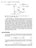
This
book
Figure 1-14: The evolution of integrated circuit design techniques, from layout level to system level
The introduction of high level description languages such as VHDL and Verilog [Verilog] have made possible
the design of complete systems on a chip (SoC), with complexities ranging from 1million to 10 million
transistors (Figure 1-14). Recently, languages for specifying circuit behavior such as SystemC [SystemC] have
been made available, which correspond to design complexity between 100 and 1000 million transistors. Notice
DEEP SUBMICRON CMOS DESIGN 1. The technology scale down
1-11 E. Sicard, S. Delmas-Bendhia 20/12/03
that the technology has always been ahead of design capabilities, thanks to tremendous advances in process
integration and circuit performances.
7. Market
Since the early days of microelectronics, the market has grown exponentially, representing more than 100 billion
€ in the beginning of the 21
st
century. The average growth in a long term trend is approximately 15%. Recently,
two periods of negative growth have been observed: one in 1997-1999, the second one in 2002. Cycles of very
high profits (1993-1995) have been followed by violent recession periods.
83 86 89 92 95 98 01 04
-20%
0
20%
Market growth (%)
Year
07
40%
2000
1995
2001
A
verage growth
Figure 1-15: The percentage of market growth over the recent years shows a long term growth of 15%
Conclusion
This chapter has briefly illustrated the technology scale down, the evolution of the microprocessor and micro-
controller complexity, as well as some general information about CMOS technology, trends and market. The
position of the Microwind layout design tool and Dsch logic design tool has been also described.
References
[Moore] G.E Moore, "VLSI: some fundamental challenges", IEEE Spectrum, N° 16 Vol 4, pp 30, 1975
[SIA] <add web site>
[Verilog] <add ref>
[VHDL] <add ref>
[SystemC] <add ref>
DEEP SUBMICRON CMOS DESIGN 1. The technology scale down
1-12 E. Sicard, S. Delmas-Bendhia 20/12/03
[Intel] <add link>
[Motorola] <add link micro-controller division>
[ITRS] <add link>
[Itoh] K. Itoh "VLSI Memory Chip Design" Springler-Verlag, 2001
EXERCISES
1. Plot the frequency improvement versus the technology for the CMOSxx technology family, using the 3-
inverter ring oscillator. Can you guess the performances of the 35nm technology?
2. Does the 3-inverter frequency performance represent the microprocessor frequency correctly? Use date of
figure 1-3 to build your answer.
3. From the 2D comparative aspect of 0.8µm and 0.25µm technologies (Figure 6), what may be the rising
problems of using multiple metallization layers?
4. With the technology scale down, the silicon area decreases for the same device (see figure 1.8), but the chip
size increases ( table 1.1). Can you explain this contradiction?
Partial answers are provided in Appendix F.
DEEP SUBMICRON CMOS DESIGN 2. The MOS devices
2-1 E. Sicard, S. Delmas-Bendhia 20/12/03
2
The MOS devices
and technology
This chapter presents the MOS transistors, their layout, static characteristics and dynamic characteristics.
Details on the materials used to build the devices are provided. The vertical aspect of the devices and the
three dimensional sketch of the fabrication are also described.
1. Properties of Silicon
IA 0
H 1
Hydro
gen
IIA III IVA VA VIA VIIA He 2
Heliu
m
Li 3
Lithiu
m
Be 4
Berylli
um
B 5
Boron
C 6
Carbo
n
N 7
Nitrog
en
O 8
Oxyg
en
F 9
Fluori
ne
Ne 10
Neon
Na 11
Sodiu
m
Mg 12
Magn
esium
IIIB IVB VB VIB VIIB VII VII VII IB IIB Al 13
Alumi
num
Si 14
Silico
n
P 15
Phos
phoru
s
S 16
Sulfur
Cl 17
Chlori
ne
Ar 18
Argon
K 19
Potas
sium
Ca 20
Calciu
m
Sc 21
Scan
dium
Ti 22
Titani
um
V 23
Vana
dium
Cr 24
Chro
mium
Mn 25
Mang
anese
Fe 26
Iron
Co 27
Cobal
t
Ni 28
Nickel
Cu29
Copp
er
Zn 30
Zinc
Ga 31
Galliu
m
Ge 32
Germ
anium
As 33
Arsen
ic
Se 24
Seleni
um
Br 35
Bromi
ne
Kr 36
Krypt
on
Rb 37 Sr 38 Y 39 Ze 40 Nb 41 Mo 42 Tc 43 Ru 44 Rh 45 Pd 46 Ag 47
Silver
Cd 48
Cadm
ium
In 49
Indiu
m
Sn 50
Tin
Sb 51 Te 52 I 53 Xe 54
Cs 55 Ba 56 La 57 Hf 72 Ta 73
Tantal
um
W 74
Tungs
ten
Re 75 Os 76 Ir 77 Pt 78 Au 79
Gold
Hg 80 Tl 81 Pb 82
Lead
Bi 83 Po 84 At 85 Rn 86
Figure 2-1: periodic table of elements and position of silicon
The table of figure 2-1 illustrates the table of elements. In CMOS integrated circuits, we mainly focus on
Silicon, situated in the column IVA, as the basic material (Also called substrate <glossary>) for all our
designs.
DEEP SUBMICRON CMOS DESIGN 2. The MOS devices
2-2 E. Sicard, S. Delmas-Bendhia 20/12/03
The silicon atom has 14 electrons, 2 electrons situated in the first energy level, 8 in the second and 4 in
the third. The four electrons in the third energy level are called valence electrons, which are shared with
other atoms.
2 electrons in 1
st
level
The Si nucleus
includes 14 protons
8 electrons in 2
n
d
level
4 valence electrons
in 3
rd
level, shared
with other atoms
Electrons repel
one another
Incomplete 3rd
level (Missing 4
other electrons)
Figure 2-2: The structure of the silicon atom
Arc
109.5°
One valence electron
to be shared with
other atoms
Figure 2-3: The 3D symbol of the silicon atom
The silicon atom has 4 valence electrons, which tend to repel each another. The 3
rd
level would be
completed with 8 electrons. The four missing electrons will be shared with other atoms. The position of
electrons which minimizes the mutual repulsion is shown in figure 2-3: each valence electron is
represented by a line with an angle of 109.5°. In order to complete its valence shell, the silicon atom tends
to share its valence electrons with 4 other electrons, by pairs. Each line between Si atoms in figure 2-3
DEEP SUBMICRON CMOS DESIGN 2. The MOS devices
2-3 E. Sicard, S. Delmas-Bendhia 20/12/03
represents a pair of shared valence electrons. The distance between two Si nucleus is 0.235 nm (10
-9
m),
equivalent to 2.35 Angstrom (10
-10
m, also represented by the letter Å).
Simple link
b
etween 2
Si atoms, distance
0.235 nm
Other Si atoms linke
d
to the central Si atom
The central Si atoms
has completed its
valence shell with 8
electrons
Figure 2- 4: The Si atom has four links, usually to other Si atoms
0.235nm
Figure 2-5: The atom arrangement is based on a 6 atom pattern
The Silicon lattice exhibits particular properties in terms of atom arrangements. The crystalline silicon is
based on a 6-atom pattern shown in figure 2-5. The structure is repeated infinitely in all directions to form
the silicon substrate as used for integrated circuit design. The pure silicon crystal is mechanically very
strong and hard, and electrically a very poor conductor, as all valence electrons are shared within the
structure (Figure 2-6). The atomic density of a silicon crystal is about 5x10
22
atoms per cubic centimeter
(cm
-3
).
DEEP SUBMICRON CMOS DESIGN 2. The MOS devices
2-4 E. Sicard, S. Delmas-Bendhia 20/12/03
The missing
valence electron
creates a hole
The free electron
moves within the
lattice
Figure 2-6: The chain of 6 atom pattern creates the silicon lattice
However, the random vibration of the silicon lattice due to thermal agitation may transmit enough energy
to some electrons valence for them to leave their position. The electron moves freely within the lattice,
and thus participate to the conduction of electricity. The lack of electron is called a hole (Figure 2-6). This
is why silicon is not an insulator, nor a good conductor. It is called a semi-conductor <glossary> due to its
intermediate electrical properties. The number of electrons which participate to the conduction are called
intrinsic carriers <gloss>. The concentration of intrinsic carriers per cubic centimeter, namely
ni, is
around 1.45x10
10
cm
-3
. When the temperature increases, the intrinsic carrier density also increases. The
concentration of free electrons is equal to the concentration of free holes.
2. N-type and P-type Silicon
To increase the conductivity of silicon, materials called dopant are introduced into the silicon lattice. To
add more electrons in the lattice artificially, phosphorus or arsenic atoms (Group VA) are inserted in
small proportions in the silicon crystal (Figure 2-7). As only four valence electrons find room in the
lattice, one electron is released and participates to electrical conduction. Consequently, Phosphorus and
arsenic are named "electron donors", with an N-type symbol. A very high concentration of donors is
coded N++ (Around 1 N-type atom per 10,000 silicon atoms, corresponding to 10
18
atoms per cm
-3
). A
high concentration of donor is coded N+ (1 N-type atom per 1,000,000 silicon atom, that is 10
16
atoms per
cm
-3
), while a low concentration of donors is called N- (1 N-type atom per 100,000,000 silicon atom, or
10
14
atoms per cm
-3
).
III
Acceptor
Add holes
P-type
IVA VA
Donor
Add electrons
N-Type
DEEP SUBMICRON CMOS DESIGN 2. The MOS devices
2-5 E. Sicard, S. Delmas-Bendhia 20/12/03
B 5 Boron C 6
Carbon
N 7
Nitrogen
Al 13
Aluminium
Si 14
Silicum
P 15
Phosphorus
Ga 31 Gallium Ge 32
Germanium
As 33
Arsenic
Figure 2-7: Boron, Phosphorus and Arsenic are used as acceptors and donors of electrons to change the
electrical properties of silicon
Boron ato
m
inserted in
the lattice
The missing valence
electron creates a hole
0.208nm
Phosphorus atom
inserted in the lattice
0.228nm
5
t
h
valence electron
of phosphorus
released in the lattice
Figure 2-8: Boron added to the lattice creates a hole (P-type property), phosphorus creates a free
electron (N-type property)
To increase artificially the number of holes in silicon, boron is injected into the lattice, as shown in figure
2-8. The missing valence link is due to the fact that boron only shares three valence electrons. The
electron vacancy creates a hole, which gives the lattice a P-type property. A very high concentration of
acceptors is coded P++ (10
18
atoms per cm
-3
) , a high concentration of acceptors is coded P+(10
16
atoms
per cm
-3
), a low concentration of acceptors is called P-(10
14
atoms per cm
-3
). The silicon substrate used to
manufacture CMOS integrated circuits is lightly doped with boron, characterized by the P- symbol. The