Điện tử học : Diod part 3 pot
Bạn đang xem bản rút gọn của tài liệu. Xem và tải ngay bản đầy đủ của tài liệu tại đây (9.41 MB, 7 trang )
Light output
p
Epitaxial layers
Substrate
n
+
n
+
Fig. 6.44: A schematic illustration of one possible LED device
structure. First n
+
is epitaxially grown on a substrate. A thin p layer
is then epitaxially grown on the first layer.
From Principles of Electronic Materials and Devices, Second Edition, S.O. Kasap (© McGraw-Hill, 2002)
E
c
E
v
E
N
(b) N doped GaP
E
g
(a) GaAs
1-
y
P
y
y < 0.45
Fig. 6.45: (a) Photon emission in a direct bandgap semiconductor.
(b) GaP is an indirect bandgap semiconductor. When doped with
nitrogen there is an electron recombination center at E
N
. Direct
recombination between a captured electron at E
N
and a hole
emits a photon.
From Principles of Electronic Materials and Devices, Second Edition, S.O. Kasap (© McGraw-Hill, 2002)
Mạch LED
LED dẫn có : V
D
= 1,6V – 2,2V; I
D
= 5 – 30mA
Chọn trung bình: V
D
= 2V và I
D
= 10 mA
Mạch có điện trở R
D
nối với LED với nguồnVcc,cách tính trò R
D
tuỳ theo trò số nguồn Vcc:
+ Vcc
R
D
I
D
Vcc = 5V R
D
= 200 Ohm Chọn 270 hoặc 330 Ohm
= 9V = 700 Ohm Chọn 680 V
D
= 12V = 1000 Ohm
D DC C D
C C D
D
D
V VR I
V V
R
I
F ro m P rin cip le s o f E le c tro n ic M a te ria ls a n d D e vic e s, S e c ond E d itio n , S .O . K a sa p (© M c G ra w -H ill, 2 002)
h ttp :// M a te ria ls .U s a sk .C a
2 eV
2 eV
eV
o
Holes in VB
Electrons in CB
1.4 eV
No bias
With forward bias
E
c
E
v
E
c
E
v
E
F
E
F
(a)
(b)
(c)
(d)
p
p
E
c
GaAs
AlGaAs
AlGaAs
p
p
n
+
~ 0.2
m
AlGaAsAlGaAs
GaAs
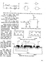
Fig. 6:46: (a) A double heterostructure diode has two junctions which
are between two different bandgap semiconductors (GaAs and
AlGaAs). (b) A simplified energy band diagram with exaggerated
features.
E
F
must be uniform. (c) Forward biased simplified energy
band diagram. (d) Forward biased LED. Schematic illustration of
photons escaping reabsorption in the AlGaAs layer and being emitted
from the device.
Ge
Si GaAs
Current
Voltage
~0.1 mA
0 0.2 0.4 0.6 0.8 1.0
Fig.6.4: Schematic sketch of the I-V characteristics of Ge, Si
and GaAs pn Junctions
From Principles of Electronic Materials and Devices, Second Edition, S.O. Kasap (© McGraw-Hill, 2002)
• LED áp dụng trong các mạch:
Chỉ báo, hiển thò
LED 7 đoạn trong các máyphát , máy đo…
Diod phát – thu hồng ngoại
Là những diod phát- diod thu quang với bức
xạ trong lãnh vực hồng ngoại .( bước sóng
khoảng1.000nm)
Được sử dụng trong các mạch báo động , điều
khiển, phát – thu tín hiệu, dữ liệu có tính bảo
mật.
8.Diod LASER
Diod khuếch đại ánh sáng bằng bức xạ của
phát xạ kích thích ( Light Amplication by
StimulatedEmission of Radiation – LASER).
Giống như diod nối nhưng có thêm bộ phận
làm đảo mật độ dân số và cọng hưỡng tạo ra
ánh sáng kết hợp có cừơng độ lớn và bức xạ
thành chùm tia tập trung rất nhỏ.
Áp dụng trong thông tin sợi quang, kênh
không gian(không giây), trong các máy CD,
VCD, DVD, mạng máy tính…