Crc Press Mechatronics Handbook 2002 By Laxxuss Episode 2 Part 7 pps
Bạn đang xem bản rút gọn của tài liệu. Xem và tải ngay bản đầy đủ của tài liệu tại đây (187.07 KB, 3 trang )
spectral response, which peaks at a wavelength about hc/E
g
. Photoresistors and junction detectors are
discussed in more detail in the following sections.
Photoresistors
The electrical conductivity of a semiconductor is the sum of two terms [5], one contributed by electrons
and the other by holes, as follows:
(19.77)
Each term is proportional to n(p) the number of electrons (holes) per unit volume in the conduction
(valence) band, the electron (hole) mobility
µ
n
(
µ
p
), and the magnitude of the charge of the electron e.
The increase in conductivity, caused by the absorption of photons increasing n and p, is the basis for the
operation of the photoresistive detector. This consists of a slab of semiconductor material on the faces
of which electrodes are deposited to allow the resistance to be monitored, as illustrated in Fig. 19.103.
The photon-induced current is proportional to the length of the electrodes and inversely proportional
to their separation, hence the typical comb-like electrode geometry of photoresistors, shown in Fig. 19.73.
Because the resistance R
C
is inversely proportional to conductivity, the variation of R
C
with incident
power P
D
is very nonlinear and is often expressed in the form
(19.78)
where a and b are constants. Cadmium sulfide is commonly used as a detector of visible radiation because
it is low cost and its response is similar to that of the human eye. Other photoconductive materials include
lead sulfide, with a useful response from 1000 to 3400 nm, indium antimonide with a useful response
out to 7000 nm, and mercury cadmium telluride with peak sensitivity in the range 5000–14,000 nm.
The wavelength range 5000–14,000 nm is of importance because it covers the peak emission from bodies
near and above ambient temperature and also corresponds to a region of good transmission through the
atmosphere. Photoconductive devices used for the detection of long wavelength infrared radiation should
be cooled because of the noise caused by fluctuations in the thermal generation of charge. As a rough
rule of thumb, because of the Boltzmann factor, a detector with energy gap E
g
should be cooled to a
temperature less than E
g
/25k.
Junction Detectors
In photoresistors, the rate of generation of electron–hole pairs by the absorption of radiation, combined
with recombination at a rate characteristic of the device, results in an increase in free charge and therefore
electrical conductivity. In junction photodetectors [6], such as photodiodes and phototransistors, newly
generated electron–hole pairs separate before they can recombine so that a photon-induced electric
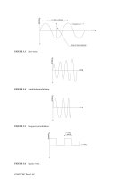
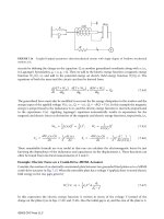
FIGURE 19.103 A simple light detector circuit employing a photoresistor is shown. An increase in light illumination
causes the resistance of the photoresistor to decrease and the output voltage to increase. The comb-like pattern
typically employed in photoresistors gives a relatively large active area of photoconducting material and a small electrode
spacing resulting in high sensitivity.
R
L
Incident
radiation
Output
voltage
Photoresistor
Bias
voltage
Evaporated
metal electrodes
Photoconducting
material
σ
ne
µ
n
pe
µ
p
+=
log
10
R
C
ablog P
D
–=
0066_frame_C19 Page 124 Wednesday, January 9, 2002 5:32 PM
©2002 CRC Press LLC
spectral response, which peaks at a wavelength about hc/E
g
. Photoresistors and junction detectors are
discussed in more detail in the following sections.
Photoresistors
The electrical conductivity of a semiconductor is the sum of two terms [5], one contributed by electrons
and the other by holes, as follows:
(19.77)
Each term is proportional to n(p) the number of electrons (holes) per unit volume in the conduction
(valence) band, the electron (hole) mobility
µ
n
(
µ
p
), and the magnitude of the charge of the electron e.
The increase in conductivity, caused by the absorption of photons increasing n and p, is the basis for the
operation of the photoresistive detector. This consists of a slab of semiconductor material on the faces
of which electrodes are deposited to allow the resistance to be monitored, as illustrated in Fig. 19.103.
The photon-induced current is proportional to the length of the electrodes and inversely proportional
to their separation, hence the typical comb-like electrode geometry of photoresistors, shown in Fig. 19.73.
Because the resistance R
C
is inversely proportional to conductivity, the variation of R
C
with incident
power P
D
is very nonlinear and is often expressed in the form
(19.78)
where a and b are constants. Cadmium sulfide is commonly used as a detector of visible radiation because
it is low cost and its response is similar to that of the human eye. Other photoconductive materials include
lead sulfide, with a useful response from 1000 to 3400 nm, indium antimonide with a useful response
out to 7000 nm, and mercury cadmium telluride with peak sensitivity in the range 5000–14,000 nm.
The wavelength range 5000–14,000 nm is of importance because it covers the peak emission from bodies
near and above ambient temperature and also corresponds to a region of good transmission through the
atmosphere. Photoconductive devices used for the detection of long wavelength infrared radiation should
be cooled because of the noise caused by fluctuations in the thermal generation of charge. As a rough
rule of thumb, because of the Boltzmann factor, a detector with energy gap E
g
should be cooled to a
temperature less than E
g
/25k.
Junction Detectors
In photoresistors, the rate of generation of electron–hole pairs by the absorption of radiation, combined
with recombination at a rate characteristic of the device, results in an increase in free charge and therefore
electrical conductivity. In junction photodetectors [6], such as photodiodes and phototransistors, newly
generated electron–hole pairs separate before they can recombine so that a photon-induced electric
FIGURE 19.103 A simple light detector circuit employing a photoresistor is shown. An increase in light illumination
causes the resistance of the photoresistor to decrease and the output voltage to increase. The comb-like pattern
typically employed in photoresistors gives a relatively large active area of photoconducting material and a small electrode
spacing resulting in high sensitivity.
R
L
Incident
radiation
Output
voltage
Photoresistor
Bias
voltage
Evaporated
metal electrodes
Photoconducting
material
σ
ne
µ
n
pe
µ
p
+=
log
10
R
C
ablog P
D
–=
0066_frame_C19 Page 124 Wednesday, January 9, 2002 5:32 PM
©2002 CRC Press LLC
20
Actuators
20.1 Electromechanical Actuators
Introduction • Type of Electromechanical
Actuators—Operating Principles • Power Amplification and
Modulation—Switching Power Electronics
20.2 Electrical Machines
The dc Motor • Armature Electromotive Force (emf) •
Armature Torque • Terminal Voltage • Methods of
Connection • Starting dc Motors • Speed Control of dc
Motors • Efficiency of dc Machines • AC
Machines • Motor Selection
20.3 Piezoelectric Actuators
Piezoeffect Phenomenon • Constitutive
Equations • Piezomaterials • Piezoactuating
Elements • Application Areas • Piezomotors (Ultrasonic
Motors) • Piezoactuators with Several Degrees of Freedom
20.4 Hydraulic and Pneumatic Actuation Systems
Introduction • Fluid Actuation Systems • Hydraulic
Actuation Systems • Modeling of a Hydraulic Servosystem
for Position Control • Pneumatic Actuation
Systems • Modeling a Pneumatic Servosystem
20.5 MEMS: Microtransducers Analysis,
Design, and Fabrication
Introduction • Design and Fabrication • Analysis of
Translational Microtransducers • Single-Phase Reluctance
Micromotors: Microfabrication, Modeling, and
Analysis • Three-Phase Synchronous Reluctance
Micromotors: Modeling and Analysis • Microfabrication
Aspects • Magnetization Dynamics of Thin
Films • Microstructures and Microtransducers with
Permanent Magnets: Micromirror Actuator •
Micromachined Polycrystalline Silicon Carbide
Micromotors • Axial Electromagnetic
Micromotors • Conclusions
20.1 Electromechanical Actuators
George T C. Chiu
Introduction
As summarized in the previous sections, a mechatronics system can be partitioned into function blocks
illustrated in Fig. 20.1. In this chapter, we will focus on the actuator portion of the system. Specifically,
we will present a general discussion of the types of electromechanical actuators and their interaction
George T C. Chiu
Purdue University
C. J. Fraser
University of Abertay Dundee
Ramutis Bansevicius
Kaunas University of Technology
Rymantas Tadas Tolocka
Kaunas University of Technology
Massimo Sorli
Politecnico di Torino
Stefano Pastorelli
Politecnico di Torino
Sergey Edward Lyshevski
Purdue University Indianapolis
0066_Frame_C20 Page 1 Wednesday, January 9, 2002 5:41 PM
©2002 CRC Press LLC