An Experimental Approach to CDMA and Interference Mitigation phần 7 potx
Bạn đang xem bản rút gọn của tài liệu. Xem và tải ngay bản đầy đủ của tài liệu tại đây (964.5 KB, 28 trang )
3. Design of an All Digital CDMA Receiver 157
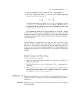
0.001
2
3
4
5
6
0.01
2
3
4
5
6
0.1
2
3
4
5
6
1
BER
1086420
E
b
/N
0
(dB)
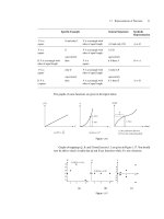
L=64, K=32
C/I=-6 dB, P/C=6 dB
J
BAID
=2
-15
AFC & PLL on
AFC & PLL off
Figure 3-60. Influence of AFCU and CPRU on EC-BAID BT performance.
Figure 3-61. Comparison between FP front end and BT front end (L = 64).
This page intentionally left blank
Chapter 4
FROM SYSTEM DESIGN TO HARDWARE
PROTOTYPING
After the previous chapter the reader should have quite clear in their mind
the main architectural solutions of the different signal detection issues which
were highlighted. The question now is how to translate it into good hard-
ware design. Introduced by a brief discussion about the main issues in
design and implementation of wireless telecommunication terminals (design
flows, design metrics, design space exploration, finite arithmetic effects,
rapid prototyping, etc.), this Chapter presents in detail the FPGA hardware
implementation of the CDMA receiver described in Chapter 3.
1. VLSI DESIGN AND IMPLEMENTATION OF
WIRELESS COMMUNICATION TERMINALS:
AN OVERVIEW
As discussed in Chapter 1, the only viable solution for handling both the
exponentially increasing algorithmic complexity of the physical layer and
the battery power constraint in wireless terminals is to rely on a heterogene-
ous architecture which optimally explores the ‘flexibility–power–
performance–cost’ design space. In this respect Figure 1-14 in Chapter 1
shows a typical heterogeneous System on a Chip (SoC) architecture employ-
ing several programmable processors (either standard and application spe-
cific), on chip memories, bus based architectures, dedicated hardware co-
processors, peripherals and I/O channels. The current trend in the design of
digital terminals for wireless communications consists in moving from the
160 Chapter 4
integration of different physical components in a system printed circuit
board to the integration of different virtual components
1
in a SoC.
As far as computational processing is concerned, we can identify three
typical digital ‘building blocks’ which are characterized by different ‘en-
ergy–flexibility–performance’ features: microprocessors, general purpose
digital signal processors (DSPs) and application specific integrated circuits
(ASICs).
A fully programmable microprocessor is better suited to perform the non-
repetitive, control oriented, input/output operations, as well as all the house-
keeping tasks (such as protocol stacks, system software and interface soft-
ware). Embedded micro cores are provided by ARM [arm], MIPS [mips],
Tensilica [tensi], IBM [ibm], ARC [arc] and Hitachi [hitac], just to name a
few.
Programmable DSPs are specialized VLSI devices designed for imple-
mentation of extensive arithmetic computation and digital signal processing
functions through downloadable, or resident, software/firmware. Their
hardware and instruction sets usually support real time application con-
straints. Classical examples of signal processing functions are finite impulse
response (FIR) filters, the Fast Fourier Transform (FFT), or, for wireless
applications, the Viterbi Algorithm (VA). We notice that conventional (gen-
eral purpose) microprocessors, although showing significantly higher power
consumptions, do not generally include such specialized architectures. DSPs
are typically used for speech coding, modulation, channel coding, detection,
equalization, or frequency, symbol timing and phase synchronization, as
well as amplitude control. Amidst the many suppliers of embedded DSP
cores, we mention here STMicroelectronics [stm], Motorola [motor], Lucent
[lucen] and Texas Instrument [ti].
A DSP is also to be preferred in those applications where flexibility and
addition of new features with minimum re-design and re-engineering are at a
premium. Over the last few years, the pressure towards low power consump-
tion has spurred the development of new DSPs featuring hardware accelera-
tors for Viterbi/Turbo decoding, vectorized processing and specialized
domain functions. The combination of programmable processor cores with
custom accelerators within a single chip yields significant benefits such as
performance boost (owing to time critical computations implemented in
accelerators), reduced power consumption, faster internal communication
between hardware and software, field programmability owed to the pro-
grammable cores and, last but the least, lower total system cost owed to the
single-DSP chip solution.
1
A ‘virtual component’ is what we may call an intellectual property (IP) silicon block. The
Virtual Socket Interface (VSI) Alliance was formed in 1996 to foster the development and
recognition of standards for designing re-usable IP blocks [vsi].
4. From System Design to Hardware Prototyping 161
ASICs are typically used for high throughput tasks in the area of digital
filtering, synchronization, equalization, channel decoding and multiuser
detection. In modern 3G handsets the ASIC solution is also required for
some multimedia accelerators such as the Discrete Cosine Transform (DCT)
and Video Motion Estimation (VME) for image/video coding and decoding.
From an historical perspective, ASICs were mainly used for their area–
power efficiency, and are still used in those applications where the required
computational power could not be supported by current DSPs.
Thanks to the recent advances in VLSI technology the three ‘building
blocks’ we have just mentioned can be efficiently integrated into a single
SoC. The key point remains how to map algorithms onto the various build-
ing blocks (software and hardware) of a heterogeneous, configurable SoC
architecture. The decision whether to implement a functionality into a hard-
ware or software subsystem depends on many (and often conflicting) issues
such as algorithm complexity, power consumption, flexibility/program-
mability, cost, and time to market. For instance, a software implementation
is more flexible than a hardware implementation, since changes in the speci-
fications are possible in any design phase. As already mentioned in Chapter
1, a major drawback is represented by the higher power consumption of SW
implementations as compared to an ASIC solution, and this reveals a crucial
issue in battery operated terminals. For high production volumes ASICs are
more cost effective, though more critical in terms of design risk and time to
market. Concerning the latter two points, computer aided design (CAD) and
system-level tools enabling efficient algorithm and architecture exploration
are fundamental to turning system concepts into silicon rapidly, thus increas-
ing the productivity of engineering design teams.
1.1 Simplified SoC Design Flow
A typical design flow for the implementation of an algorithm functional-
ity into a SoC, including both hardware and software components, is shown
in Figure 4-1. The flow encompasses the following main steps:
1. creation a system model according to the system specification;
2. refinement of the model of the SoC device;
3. hardware–software partitioning;
4. hardware–software co-simulation;
5. hardware–software integration and verification;
6. SoC tape out.
The first step consists in modeling the wireless system (communication
transmitter and/or receiver, etc.) of which the SoC device is part of. Typi-
162 Chapter 4
cally, a floating point description in a high level language such as MAT-
LAB, C or C++ is used during this phase. Recently there has been an impor-
tant convergence of industry/research teams onto SystemC
2
as the leading
approach to system level modeling and specification with C++.
Figure 4-1. Simplified SoC Design Flow.
Today most electronic design automation (EDA) suppliers support Sys-
temC. Within such a programming/design environment, high level intellec-
tual property (IP) modules being commercially available helps to boost
design efficiency and verifying compliance towards a given reference stan-
dard. Based on these IPs designers can develop floating point models of
digital modems by defining suitable algorithms and verifying performance
via system level simulations. The system model is firstly validated against
well known results found in the literature as well as theoretical results (BER
curves, performance bounds, etc.) in order to eliminate possible modeling or
2
The rationale behind the Open SystemC Initiative [syste] is to provide a modeling frame-
work for systems where high level functional models can be refined down to implementa-
tion in a single language.
System specification
Algorithms definition
and refinement
SW description HW description
Software
Design Flow
HW-SW Partitioning
Hardware
Design Flow
Co-simulation
SoC Integration (HW/SW)
and verification
SoC Tape Out
4. From System Design to Hardware Prototyping 163
simulation errors. Simulations of the system model are then carried out in
order to obtain the performance of a ‘perfect’ implementation, and conse-
quently to check compliance with the reference standard specification (i.e.,
2G, 3G, etc.). The outcomes of this second phase are considered as the
benchmark for all successive design steps which will lead to the develop-
ment of the final SoC algorithms. Currently many design tools for system
simulation are available on the market, such as CoCentric System Studio
TM
and COSSAP
TM
by Synopsys [synop], SPW
TM
by Cadence [caden], MAT-
LAB
TM
by MathWorks [mathw], etc The legacy problem and high costs
often slow down the introduction of new design methodologies and tools.
Anyway, different survey studies showed that the most successful companies
in the consumer, computer and communication market are those with the
highest investments in CAD tools and workstations.
Following the phase of system simulation, joint algorithm/architecture
definition and refinement takes place. This step, which sets the basis for
hardware/software partitioning, typically includes the identification of the
parameters which have to be run time configurable and those that remain
preconfigured, the identification (by estimation and/or profiling) of the
required computational power (typically expressed in number of operations
per second ʊ OPs), and the estimation of the memory and communication
requirements. The partitioning strategy not only has a major impact on die
size and power consumption, but also determines the value of the selected
approach for re-use in possible follow up developments. In general, resorting
to dedicated building blocks is helpful for well known algorithms that call
for high processing power and permanent utilization (FFT processors, Turbo
decoding, etc.). The flexibility of a DSP (or micro) core is required for those
parts of a system where complexity of the control flow is high, or where
subsequent tuning or changes of the algorithms can achieve later market
advantages or an extension of the SoC application field.
After partitioning is carried out the (joint) development of hardware and
software requires very close interaction. Interoperability and interfacing of
hardware and software modules must be checked at any stage of modeling.
This requires co-simulation of the DSP (or micro) processor instruction set
(IS) with the dedicated hardware. Once a dream, co-simulation is nowadays
a reality for many processors within different CAD products available on the
market, such as Synopsys [synop], Cadence [caden], Coware [cowar] and
Mentor Graphics [mento]. In particular, finite word length effects have to be
taken into account in both hardware and software modules by means of bit
true simulation. This requires the conversion of the original model from
floating to fixed point. Such a process reveals a difficult, error prone and
time consuming task, calling for substantial amounts of previous experience,
even if support from CAD tools is available (such as, for instance, the Co-
164 Chapter 4
Centric System Studio
TM
Fixed Point Designer by Synopsys). Thus the final
system performance can be assessed, the actual implementation loss
3
can be
evaluated. Even though the algorithms are modified from the original float-
ing point model, the interfaces of the SoC model are kept. The bit true model
can always be simulated or compared against the floating point one, or it can
be simulated in the context of the entire system providing a clear picture of
the tolerable precision loss in the fixed point design.
Overall system simulation is particularly relevant when different building
blocks have to evaluated jointly to assess overall performance, and no sepa-
rate requirements for the building blocks are provided. In cellular mobile
communications systems absolute performance limits are given in terms of
conformance test specifications, which indicate certain tests and their corre-
sponding results boundaries. However, standards generally specify only
overall performance figures. Let us consider, for instance, a specification for
the block error rate (BLER) at the output of the channel decoder, whose
performance depends on the entire physical layer (analog front end, digital
front end, modem, channel decoder, etc.). The standard does not provide
modem or codec specifications, but only overall performance tests. Thus no
absolute performance references or limits exist for the major sub-blocks that
can be used in the design process. This situation can be successfully tackled
by starting with floating point models for the sub-blocks. These models can
be simulated together to ascertain whether they work as required, and a
tolerable implementation loss with respect to the floating point model can
then be specified as the design criterion for the fixed point model. The final
model serves then as an executable bit true specification for all the subse-
quent steps in the design flow.
Software design flow for DSP processor typically assumes throughput
and RAM/ROM memory requirements as key optimization criteria. Unfortu-
nately, when implementing complex and/or irregular signal processing
architectures, even the latest DSP compilers cannot ensure the same degree
of optimization that can be attained by the expert designer’s in depth knowl-
edge of the architecture. As a result, significant portions of the DSP code
3
Two main issues must to be considered when dealing with finite word lengths arithmetics:
(i) each signal sample (which is characterized by infinite precision) has to be approximated
by a binary word, and this process is known as quantization; (ii) it may happen that the
result of a certain DSP operation should be represented by a word length that cannot be
handled by the circuit downstream, so the word length must be reduced. This can be done
either by rounding, by truncation, or by clipping. The finite word length representation of
numbers in a wireless terminal has ideally the same effect as an additional white noise
term and the resulting decrease in the signal to noise ratio is called the implementation loss
[Opp75]. For hardware dedicated logic the chip area is, to a first approximation, propor-
tional to the internal word length, so the bit true design is always the result of performance
degradation and area complexity trade off.
4. From System Design to Hardware Prototyping 165
need to be tuned by hand (to explicitly perform parallelization, loop unroll-
ing, etc.) to satisfy the tight real time requirements of wireless communica-
tions. Of course, this approach entails many drawbacks concerning reliability
and design time. In this respect, DSP simulation/emulation environment
plays an important role for code verification and throughput performance
assessment.
Once a bit true model is developed and verified, the main issue in the
hardware design flow is to devise the optimum architecture for the given
cost functions (speed, area, power, flexibility, precision, etc.) and given
technology. This is usually achieved by means of multiple trade offs: paral-
lelism vs. hardware multiplex, bit serial vs. bit parallel, synchronous vs.
asynchronous, precision vs. area complexity etc First, the fixed point algo-
rithms developed at the previous step are refined into a cycle true model, the
latter being much more complex than the former, and thus requiring a greater
verification effort. Refining the fixed point model into a cycle true model
involves specifying the detailed HW architecture, including pipeline regis-
ters and signal buffers, as well as the detailed control flow architecture and
hardware–software interfaces. This final model serves as a bit- and cycle
true executable specification to develop the hardware description language
(HDL) description of the architecture towards the final target implementa-
tion.
Many different HW implementation technologies such as FPGA (field
programmable gate array), gate array, standard cell and full custom layout
are currently available. From top to bottom, the integration capability, per-
formance, non-recurrent engineering cost, development time, and manufac-
turing time increase, and cost per part decreases owing to the reduced silicon
area. The selection of the technology is mainly based on production volume,
required throughput, time to market, design expertise, testability, power
consumption, area and cost trade off. The technology chosen for a certain
product may change during its life cycle (e.g., prototype on several FPGAs,
final product on one single ASIC). In addition to the typical standard cells,
full custom designed modules are generally employed in standard cell ICs
for regular elements such as memories, multipliers, etc. [Smi97].
For both cell based and array based technology an ASIC implementation
can be efficiently achieved by means of logic synthesis given the manufac-
turer cell library. Starting from the HDL (typically IEEE Std. 1076 – VHDL
and/or IEEE Std. 1364 Verilog HDL) system description at the register
transfer level (RTL), the synthesis tool creates a netlist of simple gates from
the given manufacturer library according to the specified cost functions
(area, speed, power or a combination of these). This is a very mature field
and it is very well supported by many EDA vendors, even if Synopsys
166 Chapter 4
Design Compiler
TM
, which has been in place for almost two decades, is
currently the market leader.
In addition to CAD tools supporting RTL based synthesis, some new
tools are also capable of supporting direct mapping to cell libraries of a
behavioral description. Starting from a behavioral description of the function
to be executed, their task is to generate a gate level netlist of the architecture
and a set of performance, area, and/or power constraints. This allows the
assessment of the architectural resources (such as execution units, memories,
buses and controllers) that are needed to perform the task (allocation),
binding the behavioral operations to hardware resources (mapping), and
determining the execution order of the operations on the produced architec-
ture (scheduling). Although these operations represent the core of behavioral
synthesis, other steps, for instance such as pipelining, can have a dramatic
impact on the quality of the final result. The market penetration of such
automated tools is by now quite limited, even if the emergence of SystemC
as a widely accepted input language might possibly change the trend
[DeM94].
After gate level netlist generation, the next step taking place is physical
design. First, the entire netlist is partitioned into interconnected larger units.
The placement of these units on the chip is then carried out using a floor
planning tool, whilst a decision about the exact position of all the cells is
done with the aid of placement and routing tools. The main goal is to imple-
ment short connection lines, in particular for the so called critical path.
Upon completion of placement, the exact parameters of the connection lines
are known, and a timing simulation to evaluate the behavior of the entire
circuit can be eventually carried out (post layout simulation). Whether not all
requirements are met, iteration of the floor planning, placement and routing
might be necessary. This iterative approach, however, has no guarantee of
solving the placement/routing problem, so occasionally an additional round
of synthesis must be carried out based on specific changes at the RTL level.
Once the design is found to meet all requirements, a programming file for
the FPGA technology, or the physical layout (the GDSII format binary file
containing all the information for mask generation) for gate array and stan-
dard cell technologies will be generated for integration in the final SoC
[Smi97]. Finally, SoC hardware/software integration and verification, hope-
fully using the same testbench defined in the previous design steps, takes
place and then tape out comes (the overall SoC GDSII file is sent out to the
silicon manufacturer).
Very often rapid prototyping is required for early system validation and
software design before implementing the SoC in silicon. Additionally, the
prototype can serve as a vehicle for testing complex functions that would
otherwise require extensive chip level simulation. Prototypes offer a way of
4. From System Design to Hardware Prototyping 167
emulating ASICs in a realistic system environment. Indeed, wireless systems
often have very stringent Bit Error Rate (BER) requirements. For example,
the typical BER requirement for a 2G system is approximately 10
-2
(voice
communications), whereas it may be as low as 10
-6
(multimedia) for a 3G
system. In general, the lower the BER requirements, the longer must be the
bitstream to be simulated to achieve statistically valid results
4
. As a rule of
the thumb we can assume that, in the case of randomly distributed errors, a
reliable estimate of the BER with the error counting technique can be ob-
tained by observing about 100 error events. It follows that in order to relia-
bly measure a BER of 10
-2
, about 10
4
symbols must be simulated, while a
BER of 10
-6
requires about 10
8
symbols. This can be unfeasible especially
for verification at the lowest level of abstraction. Many rapid prototyping
environment are available on the market for system emulation (such as
Cadence [Smi97], Aptix [aptix], FlexBench [Pav02], Nallatech [nalla] and
Celoxica [celox]). Alternatively, a prototyping environment can be devel-
oped in house, exploiting FPGA technology, possibly with downgrading of
speed performance with respect to an ASIC solution, but still validating the
logic functioning and hardware/software interfaces. Basing the FPGA proto-
type development exclusively on ASIC design rules, makes FPGA to ASIC
technology conversion unnecessary, and lets the design version verified in
the prototype ready for ASIC SoC implementation.
The following Sections of this Chapter present the design of the all-
digital MUSIC receiver for hardware emulation, based on a custom designed
platform. Particularly, rapid prototyping on FPGA technology for the EC-
BAID ASIC is presented. The relevant ASIC design flow for a 0.18 µm
CMOS standard cell technology will be detailed in Chapter 5.
2. FPGA IMPLEMENTATION OF THE
ALL DIGITAL MUSIC RECEIVER
Following the general design rules outlined in the previous Section, the
final architecture of the MUSIC receiver as in Section 3.4 was simulated in a
high level general purpose programming language. For legacy reasons the
scientific computation language FORTRAN was used, but the same results
would have been obtained with C or C++. Through this simulator, or through
relevant subsections, the different receiver subsections were designed and
optimized as detailed in Chapter 3.
4
All of the considerations reported here about BER estimation by means of measurement
on the hardware prototype refer to the simple error counting technique (also addressed to
as Monte Carlo method) which evaluates the error probability as the ratio between the
number of observed errors and the number of transmitted bit, within a given time interval.
168 Chapter 4
After that, the bit true, fixed point architecture of the receiver was simu-
lated by means of a parametric FORTRAN model derived from the above-
mentioned floating point simulation. The bit true model allowed determina-
tion of the wordlength of all internal digital signal as a trade off between
complexity and overall performance. Bit true and floating point perform-
ances were continually compared to satisfy the given constraint of a maxi-
mum degradation of 0.5 dB. Once this goal was achieved, the circuit was
described at the Register Transfer Level (RTL) with the VHDL (Very high
speed integrated circuit Hardware Description Language) hardware descrip-
tion language, and the resulting model was input to the subsequent logic
synthesis stage. The receiver was also equipped with extra auxiliary modules
for monitoring and control. This allowed final evaluation and verification of
the HW by means of direct comparison with the expected simulated results.
This debugging activity will be detailed later in Chapter 6.
FPGA implementation represents the final goal of the receiver front end
and synchronization loops. In contrast, it is only an intermediate phase for
the EC-BAID design ʊ it is just the stage of fast prototyping before ASIC
implementation. Rapid prototyping aims at validating the system architecture
before submission of the physical layout to the foundry. Therefore, the EC-
BAID was described in VHDL as an ASIC core, and such circuit was di-
rectly targeted to FPGA technology without any modifications. This entailed
a certain downgrading of speed performance: the FPGA implementation of
the EC-BAID circuit could properly work for a subset of the required chip
rates only, specifically from 128 kchip/s to 512 kchip/s. No pipeline registers
were added to speed up the FPGA clock frequency, since the goal of the
prototyping was testing the ASIC RTL with no changes.
A summary of the digital design flow that led to the FPGA implementa-
tion of the MUSIC receiver is sketched in Figure 4-2. This is conceptually
very close to what described in the previous Section, and almost identical to
the one that will be detailed in Chapter 5 for the ASIC implementation, with
the only exception of the target technology. As a general rule, it is good
practice in creating the design for the ASIC, first to verify and test it, and
only then to implement the changes necessary for translating the design to
FPGA technology. Operating the other way round (from FPGA design to
ASIC) is more risky. First, errors in the translation are not visible in the
prototype, and thus are not revealed in prototype testing. Second, the test
structures for ASIC (Scan Path, memory BIST, etc.) are not implemented in
the native design for FPGA. When the design is ported to the ASIC the test
structures need to be added and re-verified with another iteration on the
FPGA.
4. From System Design to Hardware Prototyping 169
Requirement
FORTRAN
Floating Point Model
FORTRAN
Simulation
FORTRAN
Test Bench
OK?
yes
no
FORTRAN
Bit True Model
FORTRAN
Simulation
OK?
yes
no
VHDL
RTL Model
VHDL
Simulation
OK?
yes
no
Macro Cell (RAM, ROM)
VHDL Model
VHDL
Test Bench
VHDL
RTL Model
Logic
Synthesis
VHDL FPGA
Gate Level Netlist
VHDL Gate Level
Simulation
OK?
yes
no
OK?
yes
no
Device Programming
VHDL Test Bench
ALTERA Library
Synthesis Constraints
ALTERA Library
Device Fitting
Interconnection Delay
VHDL FPGA
Gate Level Netlist
VHDL Gate Level
Simulation
OK?
yes
no
VHDL Test Bench
ALTERA Library
Figure 4-2. MUSIC Receiver FPGA Design Flow.
VHDL
RTL netlist
constraints
ASIC FPGA migration
VHDL
RTL netlist
constraints
Synthesis and optimization
Tool : Synopsys FPGA Compiler II
Synthesis and optimization
Tool : Synopsys FPGA Compiler II
EDIF
netlist
Final synthesis and fitting
Tool : Altera Max+Plus II
Final synthesis and fitting
Tool : Altera Max+Plus II
SOF
file
FPGA programmer
Pin assignments
Figure 4-3. FPGA re-targeting of the ASIC design flow.
170 Chapter 4
The conclusion is that when designing for an ASIC implementation the
best approach is to include test and other technology specific structures from
the very beginning (see Chapter 5 for details). When developing an RTL
code no different approaches are needed for ASIC and/or FPGA, except for
possible partitioning of the whole circuit into multiple FPGAs. The best
approach is thus using a compatible synthesis tool, so that (in principle) the
same code can be re-used to produce the same functionality. Developing a
unique code for the two designs helps increasing the reliability of the proto-
type.
Of course, technology specific macro cells, such as RAM/ROM, micro
(DSP) cores, PLLs, physical interfaces, I/Os, clock buffers, cannot be di-
rectly ported from one technology to the other, and they need manual re-
mapping. Technology specific macro cells can be classified into two catego-
ries: cells that can be implemented/modeled in FPGA technology and cells
that cannot. When migrating from ASIC to FPGA design, macro cells that
cannot be mapped directly into the FPGA (for instance, an ASIC DSP core)
need to be implemented directly on the board using off the shelf compo-
nents, test chips, or other equivalent circuits. So when developing the HDL
code it is good practice to place such macrocells into the top level, so as to
minimize and ‘localize’ the changes that are needed when retargeting to
FPGA. This approach also facilitates the use of CAD tools. In fact, by prop-
erly using the synthesis directives available within the tool, the same HDL
code can be actually used for the two technologies. The CAD recognizes
those macrocells that can/cannot be synthesized and acts according to the
specified technology.
Even macros which can be implemented in FPGA technology need a lim-
ited amount of manual re-mapping. The recommended way of doing this re-
mapping is instantiating the ASIC macro where it is needed, and then creat-
ing another level of hierarchy for instantiating the FPGA macro(s) under-
neath. Doing mapping this way allows one to re-use exactly the same code
for both designs. The EC-BAID falls in the latter case, since its ASIC design
includes only memory macros (see Section 2.2.1 for further details).
Obviously these considerations do not apply to the multi-rate front end or
to the synchronization loops, whose design was only targeted to implementa-
tion with programmable devices.
4. From System Design to Hardware Prototyping 171
2.1 FPGA Partitioning
Implementation of the MUSIC receiver was based on the DSP breadboard
called PROTEO, provided by STMicroelectronics [stm]. As detailed in
Chapter 6, the PROTEO breadboard is based on a pair of Altera FPGAs
10K100A CPLDs (Complex Programmable Logic Device), for a full integra-
tion capability of 200 Kgates. The breadboard is also equipped with a fixed
point 16 bit DSP processor (66 MIPs, ST18952 by STMicroelectronics) and
includes other features like high speed ADC converters and programmable
clock generators. The CPLDs were used for real time signal processing
functrions, while the DSP was dedicated to (low speed) housekeeping and
measurement tasks.
The overall receiver complexity exceeds the capability of a single bread-
board; on the other hand, the final goal of the project was an ASIC imple-
mentation of the EC-BAID circuit. Therefore, it was straightforward to
resort to two identical breadboards. The first PROTEO was dedicated to the
implementation of the whole receiver with the exception of the EC-BAID,
and was arranged so as to inter-operate either with a second, identical PRO-
TEO connected through a flat cable and implementing the EC-BAID func-
tions, or directly with the ASIC circuit. This solution allowed rapid prototyp-
ing of the EC-BAID circuit on FPGA first, and thorough testing of the EC-
BAID ASIC subsequently. Figure 4-4 shows the final partitioning of the
receiver, implemented either with FPGA+FPGA or with FPGA+ASIC
technology. BER measurement and SNIR estimation, as well as housekeep-
ing and initialization, are carried out by the DSP. Figures 4-5 and 4-6 show
the schematic and the appearance, respectively, of the FPGA+FPGA con-
figuration.
Preliminary synthesis runs showed that owing to the limited size
(100 kGates) of each CPLD mounted on the PROTEO breadboard a single
device implementation of the MUSIC receiver front end and EC-BAID
detector was not feasible. Hence, further partitioning of both circuits (the
front end on PROTEO I, and the EC-BAID on PROTEO II) between the two
available CPLDs was taken into account.
Since the time of this design FPGA technology has improved very much.
At the time of writing (mid 2003) FPGAs allowing the integration of more
than 1 million equivalent gates are easily available on the market, so that the
whole MUSIC receiver would surely fit into a single FPGA device. Anyhow,
the experience of system partitioning which we describe here is still valid
when thinking of a more complex and integrated multimedia terminal with
audio/video codecs and complex channel coding/decoding, according to the
general trend shown in Figure 1-11 for technology and algorithm complex-
ity.
172 Chapter 4
AD S807
ST 18952 DSP
ADC
DCO
I
Q
N-
stage
Integrator
U
N-stage
Comb
Compensation
Filter / CMF
f
s
f
s
f
d
f
d
=4R
c
'
f
ˆ
N-stage
Integrator
U
N-stage
Comb
Compensation
Filter / CMF
f
s
f
s
f
d
f
s
f
s
2
n
s
=4
Interp .
n
s
=2
2R
c
f
d
=4R
c
2
n
s
=4
Interp .
n
s
2R
I/Q Soft
Data
L
CCTU
CCAU
Prompt
-
I
Prompt
-
Q
E/L
-
I
E/L
-
Q
E/L
EC-
BAID
Unit
I/Q
Correlator
FED
Pilot Channel Code
Traffic Channel Code
Demux
-
I
Demux
-
Q
R
c
R
c
R
s
R
s
SNIR
Estimation
SNIR
R
s
Symbol
Start
Signal Detect /
Demod . Enable
AFC
Loop
Filter
Int. Clock 8R
c
IF Input
f
IF
=70 MHz
R
c
R
c
R
c
Code
epoch
Sync
AGC
Symb
.
Clock
BER
Measurem
.
P
P Interface
BER
f
s
IFd
=4.464 MHzf
Proteo II
AD S807
PROTEO-I, flex-I
ST 18952 DSP
ADC
DCO
I
Q
N-
stage
Integrator
U
N-stage
Comb
Compensation
Filter / CMF
f
s
f
s
f
d
f
d
=4R
c
'
f
ˆ
N-stage
Integrator
Quadrature
Front-End
U
N-stage
Comb
Compensation
Filter / CMF
CIC Decimation
f
s
f
s
f
d
f
s
f
s
2
n
s
=4
Interp .
n
s
=2
2R
c
f
d
=4R
c
2
n
s
=4
Interp .
n
s
2R
I/Q Soft
Data
L
CCTU
CCAU
Prompt
-
I
Prompt
-
Q
E/L
-
I
E/L
-
Q
E/L
EC-
BAID
Unit
I/Q
Correlator
FED
Pilot Channel Code
Traffic Channel Code
Demux
-
I
Demux
-
Q
R
c
R
c
R
s
R
s
SNIR
Estimation
SNIR
R
s
Symbol
Start
Signal Detect /
Demod . Enable
AFC
Loop
Filter
Int. Clock 8R
c
IF Input
f
IF
=70 MHz
R
c
R
c
R
c
Code
epoch
Sync
AGC
Symb
.
Clock
BER
Measurem
.
P
P Interface
BER
Interp .
n
s
2R
I/Q Soft
Data
L
CCTU
CCAU
Prompt
-
I
Prompt
-
Q
E/L
-
I
E/L
-
Q
E/L
EC-
BAID
Unit
I/Q
Correlator
FED
Pilot Channel Code
Traffic Channel Code
Demux
-
I
Demux
-
Q
R
c
R
c
R
s
R
s
SNIR
Estimation
SNIR
R
s
R
s
Symbol
Start
Signal Detect /
Demod . Enable
AFC
Loop
Filter
Int. Clock 8R
c
IF Input
f
IF
=70 MHzf
IF
=70 MHz
R
c
R
c
R
c
Code
epoch
Sync
AGC
Symb
.
Clock
BER
Measurem
.
P
P Interface
BER
f
s
IFd
=4.464 MHzf
PROTEO-I,
flex-II
In-Phase
Front-End
CIC Decimation
PROTEO-II/
ASIC
AD S807
ST 18952 DSP
ADC
DCO
I
Q
N-
stage
Integrator
U
N-stage
Comb
Compensation
Filter / CMF
f
s
f
s
f
d
f
d
=4R
c
'
f
ˆ
N-stage
Integrator
U
N-stage
Comb
Compensation
Filter / CMF
f
s
f
s
f
d
f
s
f
s
2
n
s
=4
Interp .
n
s
=2
2R
c
f
d
=4R
c
2
n
s
=4
Interp .
n
s
2R
I/Q Soft
Data
L
CCTU
CCAU
Prompt
-
I
Prompt
-
Q
E/L
-
I
E/L
-
Q
E/L
EC-
BAID
Unit
I/Q
Correlator
FED
Pilot Channel Code
Traffic Channel Code
Demux
-
I
Demux
-
Q
R
c
R
c
R
s
R
s
SNIR
Estimation
SNIR
R
s
Symbol
Start
Signal Detect /
Demod . Enable
AFC
Loop
Filter
Interp .
n
s
=2
2R
c
f
d
=4R
c
2
n
s
=4
Interp .
n
s
2R
I/Q Soft
Data
L
CCTU
CCAU
Prompt
-
I
Prompt
-
Q
E/L
-
I
E/L
-
Q
E/L
EC-
BAID
Unit
I/Q
Correlator
FED
Pilot Channel Code
Traffic Channel Code
Demux
-
I
Demux
-
Q
R
c
R
c
R
s
R
s
SNIR
Estimation
SNIR
R
s
Symbol
Start
Signal Detect /
Demod . Enable
AFC
Loop
Filter
Int. Clock 8R
c
IF Input
f
IF
=70 MHz
R
c
R
c
R
c
Code
epoch
Sync
AGC
Symb
.
Clock
BER
Measurem
.
P
P Interface
BER
f
s
IFd
=4.464 MHzf
Proteo II
AD S807
PROTEO-I, flex-I
ST 18952 DSP
ADC
DCO
I
Q
N-
stage
Integrator
U
N-stage
Comb
Compensation
Filter / CMF
f
s
f
s
f
d
f
d
=4R
c
'
f
ˆ
N-stage
Integrator
Quadrature
Front-End
U
N-stage
Comb
Compensation
Filter / CMF
CIC Decimation
f
s
f
s
f
d
f
s
f
s
2
n
s
=4
Interp .
n
s
=2
2R
c
f
d
=4R
c
2
n
s
=4
Interp .
n
s
2R
I/Q Soft
Data
L
CCTU
CCAU
Prompt
-
I
Prompt
-
Q
E/L
-
I
E/L
-
Q
E/L
EC-
BAID
Unit
I/Q
Correlator
FED
Pilot Channel Code
Traffic Channel Code
Demux
-
I
Demux
-
Q
R
c
R
c
R
s
R
s
SNIR
Estimation
SNIR
R
s
Symbol
Start
Signal Detect /
Demod . Enable
AFC
Loop
Filter
Int. Clock 8R
c
IF Input
f
IF
=70 MHz
R
c
R
c
R
c
Code
epoch
Sync
AGC
Symb
.
Clock
BER
Measurem
.
P
P Interface
BER
-
I
E/L
-
Q
E/L
EC-
BAID
Unit
I/Q
Correlator
FED
Pilot Channel Code
Traffic Channel Code
Demux
-
I
Demux
-
Q
R
c
R
c
R
s
R
s
SNIR
Estimation
SNIR
R
s
Symbol
Start
Signal Detect /
Demod . Enable
AFC
Loop
Filter
Int. Clock 8R
c
IF Input
f
IF
=70 MHz
R
c
R
c
R
c
Code
epoch
Sync
AGC
Symb
.
Clock
BER
Measurem
.
P
P Interface
BER
Interp .
n
s
2R
I/Q Soft
Data
L
CCTU
CCAU
Prompt
-
I
Prompt
-
Q
E/L
-
I
E/L
-
Q
E/L
EC-
BAID
Unit
I/Q
Correlator
FED
Pilot Channel Code
Traffic Channel Code
Demux
-
I
Demux
-
Q
R
c
R
c
R
s
R
s
SNIR
Estimation
SNIR
R
s
R
s
Symbol
Start
Signal Detect /
Demod . Enable
AFC
Loop
Filter
Int. Clock 8R
c
IF Input
f
IF
=70 MHzf
IF
=70 MHz
R
c
R
c
R
c
Code
epoch
Sync
AGC
Symb
.
Clock
BER
Measurem
.
P
P Interface
BER
f
s
IFd
=4.464 MHzf
PROTEO-I,
flex-II
In-Phase
Front-End
CIC Decimation
PROTEO-II/
ASIC
Figure 4-4. MUSIC Receiver Final Partitioning.
4. From System Design to Hardware Prototyping 173
Programming
FLAT CABLE
FLAT CABLE
Connection
flex-II
flex-II
flex-I
flex-II
PROTEO-I
PROTEO-II
Programming
FLAT CABLE
FLAT CABLE
Connection
flex-II
flex-II
flex-I
flex-II
PROTEO-I
PROTEO-II
Figure 4-5. Schematic of the FPGA+FPGA based configuration of the receiver.
Figure 4-6. Picture of the two interconnected PROTEO breadboards.
174 Chapter 4
2.1.1 Multi-Rate Front End and Synchronization Circuits on
PROTEO-I
Partitioning of the front end and synchronization circuits was quite criti-
cal for their final implementation, and heavily affected the resulting architec-
ture. The final mapping of functions onto the available devices was derived
as a trade off between hardware complexity and functional behavior. Ac-
cording to Figure 4-5, the first device on the left hand side of the PROTEO-I
platform, connected to the tri-states buffers that manage the incoming signal,
will be referred to as flex-I, whilst the second one will consequently be
referred to as flex-II. Flex-I was dedicated to front end functionalities: digital
downconversion to baseband, decimation by means of the CIC decimator
filter, chip matched filtering and linear interpolation. The AFC was also
placed here, in order to keep the 11 bit frequency error control signal as
close as possible to the DCO. The AFC is fed with the pilot symbols coming
from the despreader located on flex-II that are already amplitude regulated.
This prevents the use of additional despreading/amplitude correction stages
into flex-I, whose complexity figure, as is shown in the following, is crucial.
Transmission of the pilot symbol values required the implementation of a
simple serial transmission protocol between the two boards, via Parallel
In/Serial Out (PISO) and Serial In/Parallel Out (SIPO) modules located on
flex-II and flex-I, respectively. This was done to keep the number of con-
nected I/O pins as small as possible.
Similar considerations apply to
fract_del, the signal which is gener-
ated by the CCTU on flex-II and brings back to the linear interpolator lo-
cated on flex-I the information about the re-sampling epoch. However,
because of its small size (5 bits) a straightforward parallel transmission was
possible. Flex-II takes in the sample stream at rate 4R
c
(four samples per
chip interval) output by the linear (I/Q) interpolators on flex-I, and is mainly
designated to carry out coarse code acquisition by means of CTAU, and chip
timing tracking performed by the CCTU. As described in Chapter 3, the
CCTU and AFCU are equipped with the SAC unit, which complements the
coarse automatic control loop (AGC) on the IF analog board so as to keep
the signal level constant and independent of the signal to noise plus interfer-
ence ratio (SNIR). Once again, owing to restrictions on the I/O pins budget
of flex-I, the connectivity functions towards the EC-BAID circuit were
allocated to flex-II: PROTEO-II during rapid prototyping, and the plug-in
mini-board with the ASIC circuit later, were mounted on the upper left 40
pins connector of flex-II. The output of flex-II is the stream of the on time
samples at rate R
c
(chip rate) coming from the interpolators on flex-I, after
subsequent decimation. Figures 4-7 and 4-8 outline the partitioning de-
scribed above between the two CPLDs and show the relative pin-out. Some
4. From System Design to Hardware Prototyping 175
of the internal signals are highlighted, together with their respective word
length. The main configuration parameters such as
rho_CIC, elle_cod,
etc., are also reported.
Finally, both devices are connected to the DSP processor via a dedicated,
embedded bus, and a suitable interface unit (not shown in Figure 4-7 and 4-
8). Communications with the DSP is required at start up to set the proper
receiver configuration, as well as to allow for internal receiver monitoring.
These features will be described in more detail in Chapter 6.
12
12
RC
12
1212
7
Interpolator (P)
8
8
7
Interpolator (Q)
88
8
SIPO
1
1
12
AFC
12
11
DCO
8
8
Front - End
16
8
8
31
AFCenable
gammaAFC
DAC
_
outpu
t
5
outFIR
_
2Rc
_
nsat
freq_comp
data_ADC
offset_ADC
3
rho_CIC
2
elle_cod
1
12
Figure 4-7. PROTEO-I partitioning: flex-I device.
2.1.2 EC-BAID on PROTEO-II
The bottleneck of the FPGA implementation of the EC-BAID was found
to be the memory macrocells. The Altera Flex10K100A FPGA contains 12
Embedded Array Blocks (EAB), allowing the implementation of RAM
blocks of 2048 bits each. Since the EC-BAID circuit needs two different
RAMs cuts (128
u
43 and 384
u
46 bits) for a total size of 23168 bits, a single
CPLD seemed to be enough. Unfortunately the Max+Plus II
TM
(release 11)
synthesis tool can not perform optimized memory cuts whose size is not a
power of 2, so it was necessary to use both devices on PROTEO-II, splitting
the EC-BAID circuit in two units, named EC-BAID_1 and EC-BAID_2
henceforth, each one managing one memory block.
176 Chapter 4
7
7
outINT_P
7
7
outINT_Q
AGC
en_prompt
2
AGCgammaAC
Q
2
AGCgammaS
S
6
Zrif_AGC
7
7
CCTU
2
CCTUgSS
6
lambdaINF
2
CCTUgACQ
en_elate
6
lambdaSUP
7
rho_AGC
1
CCTU_lock
CEG
2
int_delay
CTAU
1
6
6
1
int_P
int_Q
8
CTAU_epoc
h
1
signal_detect
code_epoch
PISO
ZregP
19
ZregP
19
38
1
serial_enable
1
1
s_OUT
1
en_prompt
1
en_elate
1
ref_BAID
fract_del
5
CCTU_lock
signal_detect
rho_AGC
CCTU_lock
signal_detect
2
W_sel
2
L_sel
int_P
int_Q
7
7
int_P
int_Q
Figure 4-8. PROTEO-I partitioning: flex-II device.
The original VHDL unit was therefore partitioned into two sub-designs,
keeping as low as possible the number of signal buses between them. Never-
theless, the 41 bit embedded bus connecting the two FPGAs could not carry
all the signals, so that an additional flat cable was needed between the two
FPGAs on the EC-BAID PROTEO-II board.
The PROTEO-II partitioning is shown in Figure 4-9, whilst Figure 4-10
shows the arrangement of the two PROTEO breadboards (MUSIC receiver
and EC-BAID) corresponding to Figure 4-6, and the flat cable buses be-
tween the four FPGAs. In particular, Figure 4-9 shows the VHDL blocks
partitioning into the two FPGAs, along with the main internal signals. A
detailed description of the EC-BAID architecture will be outlined in Chapter
5, where its ASIC implementation is extensively addressed. In short, block 1
in Figure 4-9 is the standard correlator receiver (CR), while the additional
adaptive interference mitigation component is computed in the correlator 2;
after the sum, the output level is regulated by the local AGC (block 3). RAM
4 stores the last 3·L input samples, which are selected in turn (block 5) to
perform hardware multiplexing; the adaptive coefficient vector x is stored in
RAM 6 and is made orthogonal to the code sequence by block 7. The CPRU
4. From System Design to Hardware Prototyping 177
(block 8) performs rotation of either EC-BAID or the CR outputs; at the
output of the CPRU, multiplexer 9 routes the selected bus into the secondary
(auxiliary) output, and multiplexer 10 selects the desired output to be sent
back to the MUSIC breadboard for monitoring and testing. Hence multiplex-
ers 9 and 10 are the only blocks added in the FPGA implementation to
increase circuit observability.
As mentioned above, partitioning mainly aimed here at splitting the two
RAM blocks on two separate devices. Accordingly, RAM 6 was integrated
into flex-I of PROTEO-II along with its surrounding logic, whilst the rest of
the circuit was assigned to flex-II of PROTEO-II. The other partitioning
requirement was to keep the number of the I/O signals as low as possible to
comply with the breadboard layout. This is why multiplexers 9 and 10 are
needed to select only one output bus at a time. All buses between the two
breadboards are carried by a flat cable, which interconnects the MUSIC
receiver (flex-II in PROTEO-I) to the EC-BAID (flex-II in PROTEO-II), and
they are summarized in Table 4-1. The two FPGAs in PROTEO-II are
connected by the internal embedded board bus and by an additional flat
cable as summarized in Table 4-2.
2.2 Implementation Details
The MUSIC receiver was described hierarchically in a VHDL mixed
structural and behavioral style. Most circuit data paths were developed
through a structural description made up of high level arithmetic operators
(such as adders, comparators and so on) mixed with explicit lower level
instantiation of registers or memories. A behavioral functional description
based on VHDL processes was reserved for finite state machines and for
control units.
The design is fully synchronous in order to simplify the logic synthesis
through utilization of a unique clock tree. However, several clock rates are
requested to tick the different building blocks of the receiver. Appropriate
multi-rate timing signals were derived from the master clock of the board
with the aid of enable strobes that selects only a subset of the active edges of
the main clock. In the FPGA+FPGA configuration, PROTEO-II is actually
slaved to PROTEO-I. The master clock of the latter comes to the former
through the coaxial cable sketched in Figure 4-10. This ensure synchronous
operation of the two boards, provided that the propagation delay of the
coaxial cable is compensated for by (manual) fine tuning of the master clock
skew controller on PROTEO-II.
178 Chapter 4
Figure 4-9. EC-BAID block diagram and partitioning.
4. From System Design to Hardware Prototyping 179
-
-
-
-
Figure 4-10. Programmable breadboards layout and naming conventions.
Table 4-1. I/O signals of the two PROTEO DSP boards.
I/O signals Bits direction
Front end outputs 7 + 7 PROTEO-I PROTEO-II
Control signals 5 PROTEO-I PROTEO-II
EC-BAID outputs 4 + 4 PROTEO-II PROTEO-I
Control signals 3 PROTEO-II PROTEO-I
Table 4-2. I/O signals between flex-I and flex-II in PROTEO-II.
I/O signals bits direction Notes
X adaptive vector 10 + 10 flex-I flex-II complex signal
Detector outputs 8 + 8 flex-II flex-I complex signal
Detector inputs 7 + 7 flex-II flex-I complex signal
Code sequence chip 1 flex-II flex-I
AGC level 8 flex-II flex-I
X RAM addresses 9 flex-II flex-I
Config. parameters 9 flex-II flex-I Code length, adaptation step, etc.
Control signals 6 flex-II flex-I Enables, reset, etc.
180 Chapter 4
2.2.1 Register Transfer Level Description
Since we have pushed our partitioning as close as possible to the com-
plexity constraints on the devices, timing constraints played a key role in the
synthesis design flow. As a result our first RTL description largely missed
those constraints in a few sections of the receiver. So, as is often the case,
iterations between different design flow steps were necessary. In the follow-
ing, we summarize the main actions that were taken to satisfy our design
goals.
MUSIC Receiver Front end
As is customary practice, possible timing violations in logic paths re-
quired the insertion into the architecture of the receiver front end of several
pipelining registers. This is done to break out long combinatorial paths and
thus to keep the combinatorial delays within the due timing constraints. The
addition of properly designed registers indeed keeps the transmission delays
smaller than the worst case clock interval, but also contributes to increasing
system latency, since implementation of a certain function ends up with
requiring more (short) clock In spite of this, the front end latency was found
to be suficiently small, so that the impact on the receiver behavior was
insignificant. In this respect, particular care was devoted to the front end
sections of the receiver that process the ADC outputs in real time at the
highest rate, namely at the clock rate f
s
= 16.384 MHz, and to those operat-
ing at f
d
= 4R
c
(four samples per chip). Specifically, the CIC decimator filter,
as well as the CMF and Equalizer FIR filter, were provided with extra inter-
nal registers so as to make them operate in pipelining.
Also, each input and output port was supported by registers in order to
get rid of the delays introduced by the propagation time of the I/O pads.
Similarly, RAMs and ROMs were specifically described as fully synchro-
nous blocks: data and address buses were supported by registers, not to add
their access time to circuit data paths. In particular, two 256
u7 ROM mod-
ules were implemented on flex-I to store the first-quadrant quantized sam-
ples of the sine function in the DCO. The ROM address is the phase signal,
represented by 8 bits (equivalent to 10 bit resolution when considering the
four-quadrant extended signal), and the value is the sine amplitude repre-
sented by 7 bits (equivalent to 8 bit resolution when considering the sign). A
256
u23 bit RAM block was reserved on flex-II to store the averaged parallel
correlations in the CTAU.
As the reader may have already observed, the diverse step sizes of the
sync loops were set for simplicity to values equal to a power of two. This
eases programmability with a simple implementation. In some cases the step
sizes are switched from an initial larger value to be used for initial acquisi-
4. From System Design to Hardware Prototyping 181
tion to a smaller steady state (SS) value, yielding optimized performance
(see Chapter 3). Table 4-3 shows the mapping rule between floating point
values and the relative bit true coded quantities for the step sizes of the front
end section.
Just like step sizes, all receiver parameters such as code length, CIC deci-
mation factor, etc., were coded onto with a proper number of bits. Table 4-4
reports the relevant associations.
Table 4-3. Bit true coding of the loops step-sizes.
Step size Floating point values Bit True Coding
J
CCTU
2
-9
, 2
-8
, 2
-7
, 2
-6
‘00’, ‘01’, ‘10’, ‘11’
J
AGC
2
-5
, 2
-4
, 2
-3
, 2
-2
‘00’, ‘01’, ‘10’, ‘11’
J
AFC
2
-19
, 2
-18
, 2
-17
, 2
-16
, 2
-15
‘000’, ‘001’, ‘010’, ‘011’, ‘100’
Table 4-4. Receiver parameters mapping rule.
Parameter Floating point values Bit True Coding Description
L 32, 64, 128 ‘00’, ‘01’, ‘11’ Code length
U
CIC
2, 4, 8,
16, 32
‘000’, ‘001’, ‘010’,
‘011’, ‘100’
Decimation factor
W
128, 256,
512, 1024
‘00’, ‘01’,
‘10’, ‘11’
CTAU smoothing window
O 1.00, 1.25, 1.50, 1.75
‘00’, ‘01’,
‘10’, ‘11’
CTAU threshold
EC-BAID
The interference mitigating detector was implemented in FPGA for rapid
prototyping and verification, but it was described in RTL with the final
target of ASIC implementation. Therefore no change in the RTL description
of the circuit (which will be detailed in Chapter 5) was implemented when it
was migrated to FPGA For instance, as opposed to the multi-rate front end
design, no pipelining was introduced in the EC-BAID architecture to speed
up its clock frequency, or equivalently, the maximum data rate it could
process. This motivates the clock speed downgrading of the FPGA EC-
BAID implementation that we have already mentioned.
Special attention was also given to the arrangement of the ASIC/FPGA
pinout. The flat cable connection between PROTEO-I (receiver breadboard)
to PROTEO-II (EC-BAID on FPGA) was designed to be re-used pin by pin
when the ASIC EC-BAID implementation take the place of PROTEO-II.
The relevant cable pin assignments are listed in Table 4-5.