An Experimental Approach to CDMA and Interference Mitigation phần 9 potx
Bạn đang xem bản rút gọn của tài liệu. Xem và tải ngay bản đầy đủ của tài liệu tại đây (1.3 MB, 29 trang )
5. Interference Mitigation Processor ASIC’s Design 217
up possible asynchronous transitions. The pad cell used by all output pins is
the B2TR_TC, a 3.3V output pad with slew-rate control and a maximum DC
current of 2 mA, suited for loads up to 50 pF.
PAD
placement
PAD
placement
ICpack
Veriloggate level netlist
Verilog gate level netlist
PAD list
Blast Fusi on
Place and route phases:
• f loor planningand
macro placement
• power routing
• cell placement and
global routing
• clock tree sy nthesis
• f iller cells
• f inal routing
• parameters extraction
Verilog
post-layout
netlist
Parasitic
parameters
GDSII
layout
GDSII
layout
Formal
verification
Formal
verification
Formality
Static
Tim ing
Analy sis
Static
Tim ing
Analy sis
PrimeTim e
Post-layout
simulation
Post-lay out
simulation
VSS
Layout
finishing
Layout
finishing
OPUS
GDSII
final layout
GDSII
final layout
DRC
LVS
DRC
LVS
Calibre
Tapeout
Magma
Synopsys
Mentor
Cadence
PAD
placement
PAD
placement
ICpack
Veriloggate level netlist
Verilog gate level netlist
PAD list
Blast Fusi on
Place and route phases:
• f loor planningand
macro placement
• power routing
• cell placement and
global routing
• clock tree sy nthesis
• f iller cells
• f inal routing
• parameters extraction
Verilog
post-layout
netlist
Parasitic
parameters
GDSII
layout
GDSII
layout
Formal
verification
Formal
verification
Formality
Static
Tim ing
Analy sis
Static
Tim ing
Analy sis
PrimeTim e
Post-layout
simulation
Post-lay out
simulation
VSS
Layout
finishing
Layout
finishing
OPUS
Layout
finishing
Layout
finishing
OPUS
GDSII
final layout
GDSII
final layout
DRC
LVS
DRC
LVS
Calibre
Tapeout
Magma
Synopsys
Mentor
Cadence
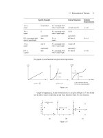
Figure 5-26. Back End design flow.
Identification of the correct number of power supply pads calls for power
consumption estimation. This was accomplished following proper guidelines
provided by the silicon foundry. A first instance, rough power estimate was
quickly calculated by Synopsys Design Compiler, which can combine the
registers switching activity monitored during an RTL simulation with statis-
tically estimated activities for the remaining combinatorial cells. This
218 Chapter 5
method resulted in an estimate of about 12 mW for the core power consump-
tion, at a clock speed of 32.768 MHz, and with a chip rate of 4.096 Mchip/s.
IOLIB_80 : 220 + 80
×
11 + 220 = 1320 µm
IOLIB_50 : 380 + 725 + 380 = 1485 µm
Figure 5-27. Die area with different pad libraries.
According to the above mentioned guidelines, 2 VDD3IOCO pads were
inserted in order to provide the 3.3 V power supply to all I/O pads, whilst 2
VDDIOCO pads were included to provide the 1.8 V power supply for the
core and the internal I/O cells buffers. Moreover, 5 VSSIOCO ground pads
were put in the remaining places. All I/O and supply pads include Electro-
Static Discharge (ESD) protections, ruling out the need for specific cells.
Pad cells were added to the netlist after the logic synthesis, while their
placement was performed as the first Back End step by means of the ICpack
tool. This software placed the pad cells taking the desired order into account
(as in Figure 5-1), and checking all the packaging rules. Its output was a
Physical Design Exchange Format (PDEF) file, which is a proprietary file
format used by Synopsys to describe placement information and clustering
of logic cells. Supplementary spaces were added between the most periph-
eral pads and the corner cells in order to avoid bonding rules violations. This
resulted in a final die area of 1528×1528 µm
2
with the IOLIB_80 pads. Start-
ing from Figure 5-27, and considering this added length and the amount of
space necessary for RAM buses routing, the 80 µm pad library still revealed
the correct choice.
In order to avoid the simultaneous switching of all the output pads, which
could impair power supply levels, additional delay cells were inserted be-
tween final registers and Outr/Outi output pads to provide a set of differ-
ent delays (however negligible with respect to the output signals symbol
rate).
5. Interference Mitigation Processor ASIC’s Design 219
3.3.2 Place and Route Flow
The whole set of Back End phases, from the synthesized gate level netlist
to the GDSII, were performed by means of Blast Fusion
TM
by Magma. This
tools was selected because it addresses circuit timing closure in a different,
more efficient way with respect to competing products available on the mar-
ket (for example, the widespread Silicon Ensemble
TM
by Cadence). Since
wire delays are becoming the predominant delay factor, a design flow that
executes placements for optimized area and then performs the routing ac-
cording to the timing constraints may require several iterations and re-
optimization phases. On the contrary, the design flow proposed by Magma
Blast Fusion
TM
addresses the timing closure problem from the very first
phases, exploiting the proprietary FixedTiming methodology together with
the SuperCell approach. Magma’s FixedTiming methodology combines
logical and physical design to ensure better performance by eliminating it-
erations between synthesis and ‘place and route’ phases. With FixedTiming,
Blast Fusion
TM
determines the optimal timing of the design prior to detailed
routing. The system then dynamically controls the size, placement and wire
interconnects of each cell to preserve the established optimal timing. This
‘correct by construction’ approach eliminates the need to re-synthesize to
improve on bad timing performance.
To achieve optimal timing, each logic cell must have the proper drive
strength for the relevant load. Because interconnect delay cannot be deter-
mined or accurately estimated during synthesis, Magma continually varies
cell sizing during place and route to maintain constant timing. Rather than
using pre-sized cells from the target library, Magma replaces each logic
function with automatically abstracted SuperCell models (functional place-
holder cells with variable sizes and fixed delay, as sketched in Figure 5-28).
Initial placement and routing of the SuperCells allows Magma to determine
the final optimal timing for all paths in the design. The layout is then com-
pleted by continuously adjusting the size of each SuperCell so that the delay
stays constant. Finally, the SuperCells are replaced with actual library cells
that have the proper drive strength. As sketched in Figure 5-29, all the place
and route tasks take place in the same tool, allowing the use a single unified
data model which is very useful for the management of large size chips.
The Verilog synthesized gate level netlist, the pad placement PDEF file,
the timing constraints set, as well as every needed library database were then
the inputs to the Blast Fusion tool. The first step accomplished within the
Magma tool was the definition of an initial floorplan with RAM blocks
placement, followed by the creation of a power routing grid in metal 5 and
metal 6. Then the cell placement, the clock
–tree synthesis, and the final rout-
ing were performed with the previously described methodologies, obtaining
220 Chapter 5
the whole ASIC layout in GDSII format. A final parasitic parameters extrac-
tion was performed to obtain a Standard Parasitic Format (SPF) file for addi-
tional post-layout timing analysis.
The resulting output from Blast Fusion flow was the GDSII layout, the
SPF parasitic parameters, a final Verilog post-layout netlist, and the related
timing exception set in Synopsys Design Constraint (SDC) format.
Figure 5-28. Magma SuperCells. Figure 5-29. Magma tasks.
3.3.3 Post-Layout Checks
After the different phases described above, several post-layout checks
were carried out by means of different tools. A static timing analysis was
carried out using Synopsys PrimeTime
TM
, which read back the final netlist
with the extracted parasitic parameters in order to check all circuit timing
requirements. A formal verification was then made with Formality
TM
by
Synopsys to ensure the logical equivalence between the starting gate level
netlist and the final post-layout netlist.
Layout checks were performed with Calibre
TM
by Mentor, consisting in a
Design Rule Check (DRC) step to control the absence of design rule viola-
tions, followed by a Layout Versus Schematic (LVS) step to check the corre-
spondence between the final gate level netlist and the actual layout.
All these final checks were correctly passed, together with a very last
Synopsys VSS
TM
gate level simulation.
3.3.4 Layout Finishing
Before tape out a final step was performed with Cadence OPUS
TM
to in-
sert all the additional elements needed by the foundry in the GDSII, like
alignment patterns, mask identification numbers, logos and external scribe
lines. A view of this final layout is shown in Figure 5-30, whilst the pack-
aged component plugged on the board to be connected to the Proteo I board
is shown in Figure 5-31.
5. Interference Mitigation Processor ASIC’s Design 221
Figure 5-30. Final EC-BAID ASIC layout.
Figure 5-31. EC-BAID ASIC mounted on the board to be connected to the PROTEO board.
222 Chapter 5
3.3.5 Design Summary
Some of the main ASIC features before packaging are listed below.
• Area: the final ASIC size is 1528 µm×1528 µm = 2.33 mm
2
.
• Speed: the worst case timing analysis reports a maximum allowed
frequency of 40 MHz, which implies a maximum chip rate of 5
Mchip/s. The range of chip rates envisaged by the MUSIC project is
thus fully covered.
• Power: a final power estimation resulted in a total power consump-
tion of 12.5 mW at the clock frequency of 32.768 MHz, with a chip
rate of 4.096 Mchip/s, which is twice the maximum chip rate speci-
fied for the MUSIC project.
• I/O timing: the setup/hold timing requirements for all the input sig-
nals with respect to the clock rising edge arrival time at the Clk pin,
as extracted by the PrimeTime analyzer, are reported in Table 5-10.
Output delays in the case of 20 pF external loads are listed in Table
5-11.
Table 5-10. Input timing requirements.
Input pin Setup time (ns) Hold time (ns)
Sym_in 0.0 0.82
Resn 0.0 0.48
Enc8 0.0 0.82
Yr 0.61 0.39
Yi 0.59 0.50
Txt 3.09 0.71
Rack 0.0 0.73
Bact 6.30 0.38
Tm 5.33 0.12
Test_si 0.10 0.64
Test_se 3.42 0.64
Table 5-11. Output delays with 20 pF loads.
Output signal Max. delay time (ns)
Req
10.16
Sym_out 11.81
Lock 24.17
Outr_3 13.20
Outr_2 13.68
Outr_1 14.94
Outr_0 16.07
Outi_3 16.35
Outi_2 18.65
Outi_1 20.34
Outi_0 22.07
Chapter 6
TESTING AND VERIFICATION OF THE MUSIC
CDMA RECEIVER
We describe in this chapter the real time testbed facility that was set up
to validate the MUSIC receiver, from the features of signal, interference and
noise generation down to the hardware architecture and the ultimate re-
ceiver performance. The ultimate purpose of the testbed was actually two-
fold: on the one hand it helped debugging the MUSIC receiver (thus getting
rid of any possible implementation bug); and tuning the diverse loop pa-
rameters. On the other, it allowed us to carry out the Bit Error Rate (BER)
performance characterization in a synthetic environment that closely mimics
the features of a typical satellite communication downlink.
1. REAL TIME TESTBED DESIGN
1.1 Overall Testbed Architecture
Repetita iuvant (repeating helps) used to say our Roman ancestors, so we
state once more that the ultimate goal of the MUSIC experiment was to vali-
date, through a proof of concept breadboard, a single-ASIC implementation
of the EC-BAID detector, as well as to demonstrate the suitability of the
whole receiver to integration into a hand held user terminal. Picture 6-1 of-
fers a view of the MUSIC testbed built up at the project facility center
[Fan01]: the master PC and several pieces of instrumentation, including the
digital boards accommodating the receiver, can be easily identified. The ac-
224 Chapter
6
tual architecture of the testbed is sketched in Figure 6-2, and its main fea-
tures are listed hereafter:
1. Flexible and programmable generation of the useful plus interfering
CDMA signal;
2. Injection of Gaussian noise with programmable level;
3. Analog IF interface between the signal generator and the MUSIC
receiver test board;
4. Interface of the MUSIC receiver to subsequent baseband processing (e.g.,
BER measurement, optional error correcting decoding, etc.);
5. Monitoring capabilities;
Signal plus Multiple Access Interference (MAI) generation is performed
via a computer controlled arbitrary waveform generator, followed by fre-
quency upconversion to the standard analog intermediate frequency 70 MHz,
and by injection of Additive White Gaussian Noise (AWGN) performed
with the aid of a precision noise generator. A master PC controls the testbed
via IEEE488 bus by means of a dedicated program specially developed in
LabVIEW. On one hand this improves configuration controllability and sys-
tem flexibility; on the other performance results in terms of BER (Bit Error
Rate), internal signals spectra monitoring, sync parameters evolution and so
on are easily attained.
Figure 6-1. A corner of the MUSIC lab.
6. Testing and Verification of the MUSIC CDMA Receiver 225
The MUSIC receiver consists of two sections, namely an IF analogue
front end, and a digital platform hosting the digital signal demodulator. The
latter is composed of two separate boards: a digital breadboard named
PROTEO, which is intended to accommodate the digital receiver front end,
as well as the slower rate ancillary functions of synchronization and house-
keeping, and a plug in mini board supporting the single ASIC implementa-
tion of the EC-BAID detector [MUS01].
The analog IF front end performs IF channel filtering via an appropriate
SAW filter, and signal amplitude automatic control to regulate the total re-
ceived power as well as a suitable level for the subsequent Analog to Digital
Converter (ADC) mounted on the digital breadboard.
NOISE
GENERATOR
to
Digital Section
RECEIVER
BOARD
AWG
1V p- p
Diff.out
Signal +
MAI
Ar bitrar y
Wa vefor m
Generator
Control
v ia IEEE488
to
Digital Section
RECEIVER
BOARD
RS 232
f
IFD
Anal og
frontend
(AGC)
MUSIC
receiver
f
IF
Signal +
MAI
UP-
converter
Noise
Ge ner ator
Signal +
MAI +
Noise
RF
Fr onte nd
Download
v ia IEEE488
f
IF
f
IF
NOISE
GENERATOR
to
Digital Section
RECEIVER
BOARD
AWG
1V p- p
Diff.out
Signal +
MAI
Ar bitrar y
Waveform
Generator
Control
v ia IEEE488
to
Digital Section
RECEIVER
BOARD
RS 232
f
IFD
Anal og
frontend
(AGC)
MUSIC
receiver
f
IF
Signal +
MAI
UP-
converter
Noise
Ge ner ator
Signal +
MAI +
Noise
RF
Fr onte nd
Download
v ia IEEE488
f
IF
f
IF
Figure 6-2. MUSIC testbed architecture.
The digital section of the receiver is shown in Figure 6-3, which displays
the PROTEO breadboard implementing the MUSIC receiver, along with the
plug in board hosting the ASIC of the EC-BAID detector.
As mentioned above, the MUSIC receiver building blocks that are ancil-
lary to the EC-BAID detector were implemented in the PROTEO bread-
board, a programmable platform specifically designed by STMicroelectron-
ics [MUS01] and whose functional block diagram is sketched in Figure 6-4.
The digital computational capability of the PROTEO breadboard mainly
relies on two Complex Programmable Logic Devices (CPLD) equipped with
100 kgates each, and provided by Altera
TM
. These devices contain program-
mable SRAM memory that is re-configurable when in the circuit, either via
226 Chapter
6
an external connector (Bit-Bluster) or by internal Flash memory. Each de-
vice also contains 624 logic units, or logic array blocks (LAB) with 8 basic
logic elements each (LE), and 24 kbit RAM memory arranged in 12 embed-
ded array blocks (EAB). The LABs are used to implement combinatory
functions such as adders, multiplexers or sequential elements, while EABs
are mainly used either for storing purpose, as for RAM and ROM, or for im-
plementation of complex functions.
Figure 6-3. Picture of the PROTEO DSP board with the EC-BAID
ASIC mini-board (upper left).
To increase system controllability and flexibility, the breadboard is also
provided with a high performance ST18952 DSP processor, operating in 16
bit fixed point arithmetic, with a worst case speed of 66 Mips/15 ns; the
ST18952 is equipped with 32K words program memory and 16.5K words
data memory.
Thanks to the proper configuration of a set of 12 bit high speed tri-state
buffers, the breadboard can be fed either via a digital input connector, or via
two ADC converters (ADS807), both interfaced to the first CPLD.
The master clock of the board is generated by a VCXO oscillator that
acts as the master frequency reference for a clock buffer/generator compo-
nent with programmable skew outputs (CY7B991). The latter generates five
separated clocks at 16.384 MHz that are user-controllable skewed (
r
6 time-
units) by a hard wired, pull up or pull down, set of resistors.
6. Testing and Verification of the MUSIC CDMA Receiver 227
Figure 6-4. PROTEO breadboard functional block diagram.
CPLD
Flex
10K100A
16bit
DSP
ST18952
JTAG
IEEE 1149.1
O
State
Anal.
/ other
12bit
ADC
Clock Gen.
&
Skew Mng.
Vcxo
ext.
CLK1
Dual
DAC
AGC1
AGC2
O
SRAM
D Mem.
64Kx16
FLASH
P Mem.
4Mx16
SRAM Mem.
256Kx16
IF /
I in
I
Q in
I
Buffer
Buffer
12bit
ADC
Buffer
I
Amp.
Amp.
CPLD
Flex
10K100A
Prog.
Clock1
Prog.
Clock2
Xtal
27MHz
Bit
Blaster
Dual
DAC
Voltage Reg.
VCC
5V
VDD
5V
CPLD
3V3
DSP
3V3
IF Dig. In
MAX7032
Bus
Switch
YBus
AFC
option
ext.
CLK2
2Vpp
2Vpp
12
12
12
12
12
Fs=16.484MHz
ADS807
ADS807
OPA2681
OPA2681
A
B
A
B
Vz
AD5323
AD5323
4
4
Glob.
CLK1
Glob.
CLK1
Glob.
CLK2
Glob.
CLK2
36
FRef
Fo1
Fo2 Fo3
Fo4
Fo5
Set Pull Up/Down Resistors
CY7B991
16.484MHz
Fout=
Fo3*(M/N)
Fout=Fo4*(M/N)
P-on
Reset
RESET
IBus
XBus
Interrupts
& Flash Mng.
74LCX245
74LCX245
74LCX245
CY7C1041V33
STM29W800
38
72
5
CPLD
Config.
DATA
Ext. Board Prog.
5
3
3
8
8
8
16
16
16
ICD2053B
ICD2053B
I/O
6x40pin
conn.
to/from
Ext.Board
(e.g.EC-BAID)
32
CY7C1021V
from PC/WS
Enable
+
Data/Cntrl
QS3R384
Ext. Memory Module
(optional)
TL7702
SUPPLY
+12V/+5V
228 Chapter
6
Moreover, additional programmable clock generators (ICD2053B, digital
PLLs) allow the generation of any clock frequency in the range 391 KHz to
90 MHz ‘on the fly’.
A large amount of memory, for general purpose processing, is available
to both CPLDs. A 256 kbit SRAM chip is connected to the first one, whilst a
SIMM-like connector for a SRAM 1MB plug in module is connected to the
second.
A comb of 40 pin headers encircles both CPLDs, allowing digital signals
monitoring, as well as external I/Os connection for additional ‘plug in’ ex-
tension boards (for example, the smaller board where the EC-BAID ASIC
device is mounted). Two more 40 pin headers, connected to the second
CPLD, are also compatible with the HP5600 State/Logic analyzer probes.
Finally a set of chips provides regulated levels of voltage in the range
3.3-5 V to supply the breadboard.
1.2 CDMA Signal Generation
The CDMA signal for the testing of the MUSIC receiver is generated as
follows [MUS01]. First, a FORTRAN computer simulation is run off-line in
order to provide a properly sampled version (with floating point amplitude
resolution) of the desired waveform spanning a given number of symbol in-
tervals. The sampling frequency of the simulated signal is
384.16
s
f MHz,
which keeps some degree of symmetry between transmit and receive clock
speeds. The available bit and chip rates of the CDMA signal are shown in
Table 6-1.
The parameters of the CDMA signal are passed to the FORTRAN pro-
gram by means of a friendly Graphical User Interface (GUI), suitably devel-
oped using the National Instruments’ LabView environment. Such a solution
allows for a quick and easy re-configuration of the test signal parameters,
thus yielding a maximum of flexibility. The GUI outputs a file containing all
the parameters of the CDMA signal, and such file is used as input by the
FORTRAN simulator. The simulation program, in addition to generating a
pseudo-random bit sequence for the useful channel bit stream, also performs
frame formatting. In particular it adds a pattern of 24 QPSK symbols (48
bits), the so called Unique Word (UW), at the beginning of the simulated
waveform for frame synchronization purposes at the receiver side.
The FORTRAN program outputs two files: a binary file containing the
signal samples (represented on 16 bits, fixed point) to be handled by the Ar-
bitrary Waveform Generator (AWG), and an ASCII text file containing the
stream of the transmitted information symbols, to be used jointly with the
data estimates provided by the receiver for BER measurement. The wave-
form obtained by computer simulation is a CDMA signal compliant with al
6. Testing and Verification of the MUSIC CDMA Receiver 229
MUSIC specifications and modulated onto a first Intermediate Frequency
(IF). Since the signal is in digital form such a frequency is referred to as
Digital IF (IFD), and is set to
464.4
IFD
f
MHz (see Figure 6-5).
Table 6-1. Values of R
c
, (kchip/s) R
b
(kbit/s) and L for the MUSIC signal.
R
b
n L = 32 n L = 64 n L = 128
2 4 R
c
= 128 2 R
c
= 128 1 R
c
= 128
8 R
c
= 256 4 R
c
= 256 2 R
c
= 256
16 R
c
= 512 8 R
c
= 512 4 R
c
= 512
32 R
c
= 1024 16 R
c
= 1024 8 R
c
= 1024
64 R
c
= 2048 32 R
c
= 2048 16 R
c
= 2048
4 2 R
c
= 128 1 R
c
= 128 R
c
=
4 R
c
= 256 2 R
c
= 256 1 R
c
= 256
8 R
c
= 512 4 R
c
= 512 2 R
c
= 512
16 R
c
= 1024 8 R
c
= 1024 4 R
c
= 1024
32 R
c
= 2048 16 R
c
= 2048 8 R
c
= 2048
8 1 R
c
= 128
2 R
c
= 256 1 R
c
= 256
4 R
c
= 512 2 R
c
= 512 1 R
c
= 512
8 R
c
= 1024 4 R
c
= 1024 2 R
c
= 1024
16 R
c
= 2048 8 R
c
= 2048 4 R
c
= 2048
16 1 R
c
= 256
2 R
c
= 512 1 R
c
= 512
4 R
c
= 1024 2 R
c
= 1024 1 R
c
= 1024
8 R
c
= 2048 4 R
c
= 2048 2 R
c
= 2048
32 1 R
c
= 512
2 R
c
= 1024 1 R
c
= 1024
4 R
c
= 2048 2 R
c
= 2048 1 R
c
= 2048
64 1 R
c
= 1024
2 R
c
= 2048 1 R
c
= 2048
f (MHz)
f
IFD
B
IF
A
A/2
S(f)
~3.21 ~4.46 ~5.71
Figure 6-5. Spectrum of the CDMA signal generated by computer simulation.
The 16 bit digitized simulated waveform (including the pseudo-random
230 Chapter
6
stream of information symbols and the UW) is then saved into a binary file
that is subsequently loaded into the memory bank of an AWG computer
board. The AWG is National Instruments’ PCI-5411 and is inserted into a
PCI slot of the master PC. It has an 8 Msample RAM, whereby each sample
is represented on 16 bit (and the overall number of stored samples must be a
multiple of 8). Also the rate of digital to analog conversion (DAC) can be set
to 20 or 40 Msample/s.
The AWG reads the samples in digital format from the memory at fre-
quency
20
AWG
f MHz. Such a value is imposed by the characteristics of
the board and cannot be easily modified. Therefore, the simulation program
features interpolation of the signal samples generated at 16.384 MHz to ‘re-
sample’ them at 20 MHz.
The number of stored digital samples per chip interval is then
/
cc
ÁWG
Nf R , (1.1)
and the number of stored samples per symbol interval turns out to be
2/
s
sAWG AWGb
NTf f R
. (1.2)
Taking into account that the RAM storage capability is 8 Msample, the
maximum number of samples stored in the AWG memory amounts to
max
8/ /5
sb
NMNR
. (1.3)
The values of N
s
and N
max
are reported in Table 6-2, for different values
of the bit rate.
Table 6-2. Values of N
max
and N
sps
as a funcion of R
b
.
R
b
(kbit/s) N
max
N
s
2 400 20000
4 800 10000
8 1600 5000
16 3200 2500
32 6400 1250
64 12800 625
In order to generate a test waveform with arbitrary duration, the file con-
taining the signal samples s
k
must be read cyclically by the AWG. Therefore
special care must be devoted to ensuring continuity of the signal at the edges
of the frame. In particular, the tails of the pulses at the end of the frame must
be ‘wrapped around’, so as to make the signal appear periodic. Considering
the UW, the total number of symbols transmitted in every frame by the
AWG is N
MEM
= N
S
T
X
+ 24, where N
S
T
X
represents the number of information
6. Testing and Verification of the MUSIC CDMA Receiver 231
symbols. Also, because of the wrap around issue, the total number of sym-
bols generated by the FORTRAN simulator is increased by 3 (Figure 6-6),
both to accommodate possible signal delays up to one symbol interval, and
to keep into account the tails of the chip pulses in the last symbol of the
stream.
When the samples stored in the memory bank are read cyclically, the
generated waveform turns actually out to be periodic, but, by carefully se-
lecting the length and kind of the symbols pattern within each period, it can
be considered as a random signal to a good approximation. This can be ac-
complished by using a maximal length pseudo-noise (PN) sequence as the
bit stream. The PN sequences have a repetition period 12
q
PN
L , with q
any integer, and this implies L
PN
< N
MAX
. The parameters of the data genera-
tor polynomials are reported in Table 6-3.
NsTx
1 2 3 . . . . . . . . . . . . . . 24 1 1 2 3
NsTxNsTxNsTx
1 2 3 . . . . . . . . . . . . . . 24 1 1 2 3
Figure 6-6. Wrap around in the generation of the waveform.
Table 6-3. Parameters of the generator polynomials.
Symbol
number
N
MAX
Code
period
L
PN
Bit rate
R
b
(kbit/s)
Taps Generator polynomial
of the useful channel’s
data (PN1)
Generator polynomial of
the interfering channels’
data (PN2)
400 255 2 8 8,4,3,2 8,6,5,3/8,6,5,2/8,7,6,5,2,1
800 511 4 9 9,4 9,6,4,3/9,8,5,4
1600 1023 8 10 10,3 10,8,3,2
3200 2047 16 11 11,7,3,2 11,8,5,2
6400 4095 32 12 1,6,4,1 12,9,3,2
12800 8191 64 13 13,4,3,1 13,10,9,7,5
The data stream of the I-component of the useful signal is given by the
PN1 sequence, whilst the stream of the Q-component is given by the PN1
sequence shifted by half a repetition period of the sequence itself. The I-
component of the generic CDMA interferer is given by the PN2 sequence
with a different shift for each user. The interfering Q-component data
streams are obtained by shifting of half a period the sequences of the rele-
vant I-component streams. The number of signal samples stored in the mem-
ory of the AWG must be a multiple of 8, and in some cases this requires a
Transmitted Symbols
232 Chapter
6
modification (i.e., shortening) of the code period. Table 6-4 presents the pa-
rameters of the data generators together with the relevant AWG memory oc-
cupancy.
In the following, each period of the transmitted waveform generated by
the AWG will be denoted as a frame, each frame starting with a UW con-
taining 24 known symbols. The AWG outputs an analog waveform y(t)
which undergoes DAC aperture compensation and low pass anti-image fil-
tering. In Figure 6-7 the interpolation filter P(f) which equalizes the aperture
distortion introduced by the DAC is shown inside the AWG, but in reality it
is implemented off-line in the FORTRAN simulation, before the waveform
actually undergoes DAC.
Table 6-4. Parameters of the data sequence generators and memory occupancy.
Symbol
number
N
MAX
Length of the
code period
plus UW
Length of the
modified code
period plus UW
Bit rate R
b
(kbit/s)
Number of
stored samples
Occupied mem-
ory (Mbyte)
400 255 + 24 255 + 24 2 5580000 10.64
800 511 + 24 511 + 24 4 5350000 10.2
1600 1023 + 24 1023 + 24 8 5235000 9.98
3200 2047 + 24 2046 + 24 16 5175000 9.87
6400 4095 + 24 4092 + 24 32 5145000 9.81
12800 8191 + 24 8184 +24 64 5130000 9.78
CLOCK
PULSE
GENERATOR
sk
fs
INTERPOLATION
FILTER P(f)
PC
y(t)x(t)
AWG
LOW-PASS
FILTER M(f)
Figure 6-7 Sketch of the computer-based CDMA test signal generation.
Figure 6-8 shows the (chip time) eye diagram of a single-user CDMA
signal generated during a preliminary validation run of the FORTRAN simu-
lator. We will also show its spectrum in next sections.
After digital to analog conversion performed at the AWG output, an ac-
tive mixer based upconverter brings the transmitted signal from the digital
intermediate frequency
IFD
f to the desired standard intermediate frequency
6. Testing and Verification of the MUSIC CDMA Receiver 233
70
IF
f MHz. The upconverter makes use of a Local Oscillator (LO) with
frequency
536.65
IFDIFLO
fff MHz. (1.4)
Figure 6-8. Eye diagram of a single CDMA signal (R
b
= 4 kbit/s, R
c
= 256 kchip/s, L = 128).
The image replica arising from the upconversion process is suppressed by
means of an analog SAW filter with fixed bandwidth of 2.5 MHz, to take
into account of the maximum signal bandwidth.
Finally, a precise amount of noise is added to the transmitted signal to re-
produce the typical impairment of a satellite channel (downlink) scenario.
The testbed relies on the wide band white Gaussian noise generator/adder,
UFX7107 by NoiseCom
TM
. Its output signal is almost flat in the range
0
–100 MHz and its spectral power density is set with 0.1 dB accuracy.
1.3 The Master Control Program
A key role in the MUSIC testbed is played by a custom developed Lab-
VIEW application, which control over every phase of the MUSIC experi-
ment [MUS01].
LabVIEW is a programming environment which was originally con-
ceived to build up applications for process control and remote measurement
with a simple, quick and flexible graphical user interface. Later, it developed
into a powerful environment that allows the development of general purpose
programs (including control, GUI development and so on) in the form of
block diagrams instead of a series of written statements as in ordinary high
level languages. A wide collection of predefined libraries provides the pro-
grammer with lot of functions for data acquisition, analysis, display and
234 Chapter
6
storage, by means of either GPIB (General Purpose Interface Bus) or serial
ports. Programs written in Labview are also referred to as virtual instruments
(VIs) since they emulate real instrumentation, both in the appearance and in
the operating mode.
The interconnection between PC and pieces of instrumentation is based
on the GPIB standard developed by Hewlett Packard in two versions (IEEE
488-1975 and the IEEE 488.2-1987) operating at 1 Mbyte/s. The GBIP bus
is implemented also in the National Instruments devices.
The LabVIEW master control application running on the master PC of
Figure 6-2 sets up the CDMA transmitter and downloads the output of the
FORTRAN simulation to the AWG board. As far as signal generation is
concerned, the testbed operator can set the number of active channels, the
chip and bit rates, the code length and type, and the number of active users.
The roll off factor of the chip pulse shaping filter can be set as well. A sam-
ple interface screen for the CDMA generator is shown in Figure 6-9. The
‘advanced settings’ panel shown in Figure 6-10 allows us to individually set
the features proper of any interfering signal, such as signature sequence
identifier and normalized delay, frequency and phase offset and power ratio
with respect to the useful channel.
Figure 6-9. Master control program GUI for modulator parameters setting.
The Master control application also sends out all signal configuration pa-
rameters to the receiver board via an RS232 connection. Figure 6-11 shows a
sample screen of the receiver configuration to be sent to the PROTEO board
[Fan01], [De03a]. After receiver configuration and set up is done, a proper
calibration procedure is automatically started by the Master control program
6. Testing and Verification of the MUSIC CDMA Receiver 235
to ensure that the values of the desired SNR and signal to interference ratio
are correctly set. Calibration is based on a set of measurements carried out
via the spectrum analyzer and controlled via GPIB by the master PC.
EQUI. POW ER
POWER (dB/ref. ch.)
UNIFORM
DELAY (symbols)
UNIFORM
PHASE (deg)
UNIFORM
FREQUENCY (Hz)
0
1
2
3
4
5
6
7
8
9
10
11
6.00
6.00
6.00
6.00
6.00
6.00
6.00
6.00
6.00
6.00
6.00
6.00
6.00
C/I dB
clear
0
1
2
3
4
5
6
7
8
9
10
11
INTERFERENCE SETUP PANEL
Wed, Jun 21, 2000
clear
show graph.
1
2
3
4
5
6
7
8
9
10
11
0
240.00
264.00
288.00
24.00
48.00
72.00
96.00
120.00
144.00
168.00
192.00
216.00
clear
1
2
3
4
5
6
7
8
9
10
11
0
clear
13.33
20.00
26.67
33.33
40.00
46.67
53.33
60.00
66.67
73.33
80.00
6.67
100.00
'
f2 (H z)
0.00
'
f1 (H z)
RANDOM
INTERF. CHANNEL #
1
2
3
4
5
6
7
8
9
10
11
0
clear
17
REF. CHANNEL #
8
Pilot
#
14
25
22
18
23
12
28
31
3
1
26
4
0.60
0.67
0.73
0.80
0.07
0.13
0.20
0.27
0.33
0.40
0.47
0.53
OK
100.00
'
f (H z)
Figure 6-10. Master control program GUI interference advanced setting.
Figure 6-11. Master control program GUI for receiver parameters setting.
After set up and calibration the receiver derives the code, carrier, and
framing references and starts decoding the incoming data stream, so that the
Master control application can start the BER performance evaluation proce-
236 Chapter
6
dure. The DSP on the PROTEO breadboard is the unit in charge of accom-
plishing this task through a procedure of direct error counting. Specifically,
it compares the transmitted bits (as read from the relevant file produced by
the FORTRAN simulator and sent via RS232 to the receiver board) with
their estimates as derived by the EC-BAID detector.
The 24 symbol UW is also used to resolve the ambiguity inherent to the
process of carrier phase estimation. As described in Chapter 3, the conven-
tional QPSK phase detector used for the MUSIC receiver suffers form a
phase ambiguity of
2/
S
, which is solved with aid of the UW as follows:
once the location of the UW is found through a non-coherent algorithm the
DSP performs all possible
2/
S
-multiple counter-rotations of the symbol
stream coming from the EC-BAID demodulator in the UW period, and com-
pares the respective results with what they should be in the absence of phase
error, to find out the most likely.
Eventually the BER measurements are sent back to the master PC where
they are post-processed by the LabVIEW Master control application for
visualization.
2. TESTBED MONITORING AND VERIFICATION
The FPGA implementation of the MUSIC receiver was carefully tested
by means of an accurate debugging procedure that aimed at demonstrating
the perfect match between the outputs of the synthesized circuits and their
RTL descriptions. In other words, the objective of this activity was to dem-
onstrate that no failures occurred during the digital synthesis design flow
addressed in Chapters 4 and 5. To accomplish this task the receiver was
equipped with additional modules especially conceived to increase system
controllability and monitoring (e.g., additional plug in boards interfaced to
the CPLD headers).
In addition to allowing preliminary debugging, such monitoring re-
sources also permitted enhanced testability and control of the receiver status
during operation [MUS01].
2.1 Testbed Debugging Features
Before going into foundry with the EC-BAID ASIC, the specific detector
and the general receiver design were verified by means of an especially de-
signed HW test bench. In particular, two identical breadboards, henceforth
called PROTEO-I and PROTEO-II were used. The first one (PROTEO-I)
was dedicated to the implementation of the multi-rate front end, whilst the
second one was temporarily used for a preliminary FPGA-based implemen-
6. Testing and Verification of the MUSIC CDMA Receiver 237
tation of the EC-BAID detector [MUS01]. In the very first testing and de-
bugging stage PROTEO-II, acting as the test bench breadboard, was also
used to host a programmable finite state machine (FSM) pattern generator to
feed PROTEO-I (under test) with the samples of an arbitrary stimulus, and to
gather the related output; the latter was then compared with the expected
waveform, as obtained by bit true computer simulations. The boards were
connected through flat ribbon cables and the input stimuli, as well as the ex-
pected outputs, were stored in two dedicated ROM memories of the test
bench board.
2.1.1 Multi-Rate Front End Verification
During verification of the multi-rate front end accommodated in the
PROTEO-I board, the EABs of the test bench board (PROTEO-II) were
loaded with the samples of a CDMA signal segment, as generated by the
FORTRAN bit true simulator. The maximum allocable memory in a single
CPLD device is 2 Kbyte, so that only 2048 8 bit input samples could be
stored. Verification was carried out at the maximum chip rate
2048
max,
c
R
kchip/s, in order to strain the data paths as much as possible.
Assuming the code length L = 64 and considering 8 samples per chip, it turns
out that only 4 data symbols can be stored in a single ROM.
The most significant observable digital signals in the multi-rate front end
are the In Phase (I) and Quadrature (Q) interpolator outputs. They are up-
dated at the rate
81924
c
R MHz (every other master clock period). This
feature may be exploited by introducing time multiplexing, thus both I and Q
components can be alternatively compared with the expected waveforms
produced by the FORTRAN bit true simulator and stored in the EABs on the
test bench board.
The outcome of the front end verification is shown in Figure 6-12 and
Figure 6-13, where the flag
compare_out, output by the FSM, is reported
as displayed on the oscilloscope screen and on the waveform viewer of the
Synopsys VSS simulation tool, respectively. This is the result of the logical
comparison between the multiplexed output of the interpolators described
above, and the relevant expected waveform: a logical value ‘1’ denotes
equality. Why is it that this signal goes to 0, then to 1 again with a few in-
termediate spikes? The reason is that both figures present a close up of what
happens at the end of the test, when the input stimulus signal out of the
ROM is zeroed, and the expected signal is zeroed as well. The output signal
cannot abruptly go to zero because of the presence of the front end filters, so
it actually reaches zero after a transient period due to the tails of the filters
response. Therefore the flag jumps again to 1 at the end of this transient pe-
riod. The intermediate spikes are the result of the filter output occasionally
238 Chapter
6
passing through zero, and thus compare_out signals a ‘false equality’.
Nevertheless, the FSM freezes the value of
compare_out into flag match
(also reported in Figure 6-13) just before the beginning of the transient, not
to affect the result of the test.
Figure 6-12. Close up of signal compare_out on the oscilloscope screen.
Figure 6-13. Front end verification on the Synopsys waveform viewer.
2.1.2 Synchronization Loops Verification
Once the front end was successfully verified, the acquisition and tracking
loops, implemented by the CTAU and CCTU (with their ancillary SAC unit)
were also verified. In order to make the test long enough to correctly stimu-
late these units, the code length was set to L = 32, and the chip rate was the
maximum allowed, namely, 2048
max,
cc
RR kchip/s. The sync loops are
6. Testing and Verification of the MUSIC CDMA Receiver 239
directly fed with the interpolated signal at rate
c
R4 , therefore the ROM
memory storing the input stimulus spanned 8 symbol periods. After the
CTAU has performed coarse code acquisition, the CCTU loop initiate chip
timing tracking, and starts producing the two control signals
fract_del
and int_del, corresponding to parameters
k
L
and
k
P
, respectively (see
Chapter 3).
Two signals can be selected, according to the value of the configuration
bit
test_sel, to be compared for testing purpose in the test bench board,
namely, either the 7 bit AGC gain
rho_AGC, or the 7 bit composite signal
obtained by concatenation of
fract_del (most significant 5 bits) and
int_delay (least significant two bits).
The FSM compares the selected signal (one sample per symbol period)
with the waveforms predicted by the Fortran bit true simulator. To achieve
further testing flexibility, and stress the CCTU loop, a 2 bit parameter
test_mode was also introduced. The permitted values are ‘00’ (mode 0),
‘01’ (mode 1) and ‘11’ (mode –1). In mode 0 the FSM cyclically reads the
ROM input memory; in mode
1 ( 1 ) the first sample of the memory is
read twice (not read) every 32 full reading cycle, so that the CCTU synchro-
nization loop has to track a T
c
/8 delay (advance) every 32 8 256 symbols.
The digital AGC gain is reported in Figure 6-14 and Figure 6-15 as re-
trieved from the hardware test bench and as expected from software simula-
tions, respectively, both in mode 0. The test window is 2048 symbol periods
long, which is 32 ms at the symbol rate
64
s
R Ksymb/s. The initial low
level in the AGC transient is owed to the initial receiver reset, whilst the in-
termediate one before the testing start, is caused by waiting for signal syn-
chronization from CTAU. Finally, after test completion the AGC gain
straight grows toward saturation, because no signal to be regulated is pre-
sented at the SAC input.
Figure 6-16 and 6-17 depict
fract_del in mode 1 as it is displayed on
the scope, as well as derived from SW simulations. In test mode 1 one input
sample is read twice every 256 symbols, which means every
4/256
s
R
ms, therefore the CCTU loop has to follow the signal delay of
4/
c
T every 8 ms, which occurs four times in the considered observation win-
dow.
2.1.3 EC-BAID Verification
Once synthesized into the FPGAs of PROTEO-II, the EC-BAID circuit
was tested separately from the MUSIC receiver to ensure perfect matching
between the desired ‘bit true’ model and the FPGA implementation. The
PROTEO-I breadboard was loaded with the hardware test bench conceived
to generate the chip rate input samples and to retrieve the EC-BAID outputs.
240 Chapter
6
Proper software running on the DSP was in charge of verifying the match
between the hardware outputs and the expected values. Particularly, 1024
chip long test vectors were generated by the FORTRAN software and stored
in the PROTEO-I RAM to be circularly sent to the PROTEO-II (EC-BAID)
breadboard, whereas the DSP was in charge of storing and comparing up to
16304 output values. Several tests, reported in Table 6-5, were performed to
validate the implementation of the various EC-BAID blocks, and all of them
were successfully run. Particularly, in the last two tests some timing re-
alignment operations (which are likely to happen in a realistic environment)
were also successfully emulated.
Figure 6-14. AGC gain rho_AGC transient as displayed on the scope (mode 0).
128
112
96
80
64
48
32
16
0
U
AGC
204817921536128010247685122560
Time (Symbols)
Test-Mode 0
L = 32
R
c
= 2048 Kchip/s,
R
b
= 64 Kbit/s
Figure 6-15. AGC gain rho_AGC transient retrieved from Fortran simulations (mode 0).
6. Testing and Verification of the MUSIC CDMA Receiver 241
According to the Static Timing Analysis results reported in Chapter 4,
this EC-BAID FPGA implementation properly worked at all the chip rates
up to 512 kchip/s; the same preliminary tests also confirmed that the FPGA
circuit did not work at
R
c
= 2048 kchip/s, whereas it actually worked at
1024
c
R
kchip/s in spite of the (conservative) theoretical timing analysis.
The chip rate of 512 kchip/s was then chosen for all functional tests with
both the MUSIC receiver and EC-BAID breadboards reported in Table 6-5.
Figure 6-16. CCTU fract_del AS displayed on the scope (mode 1).
32
28
24
20
16
12
8
4
0
fract_del
204817921536128010247685122560
Time (Symbols)
Test-Mode +1
L = 32
R
c
= 2048 Kchip/s,
R
b
= 64 Kbit/s
Figure 6-17. CCTU fract_del derived by Fortran simulations (mode 1).
2.2 Debugging the MUSIC Receiver
Once the PROTEO-II board with the FPGA implementation of the EC-
BAID is tested in a stand-alone mode joint testing of the two boards with