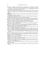
Lumped Elements for RF and Microwave Circuits phần 3 ppsx
Bạn đang xem bản rút gọn của tài liệu. Xem và tải ngay bản đầy đủ của tài liệu tại đây (1.38 MB, 51 trang )
82 Lumped Elements for RF and Microwave Circuits
Figure 3.18 Two-level inductor fabricated using (a) metal 5 and metal 4 and (b) metal 5 and
metal 3 layers. (From: [42]. 2001 IEEE. Reprinted with permission.)
Table 3.7
Approximate Parasitic Capacitance Between Metal Layers and Metal and Si Substrate
C
1
(pF/
m
2
) C
2
(pF/
m
2
)
Metal A Metal B Metal A–Metal B Metal B–Substrate C
eq
(pF/
m
2
)
M
5
M
4
40 6 14
M
5
M
3
14 9 5.4
M
5
M
2
9 12 4.0
M
i
designates the metal i layer.
where L
t
is the total inductance of the stacked inductor. From Table 3.7 it is
obvious that the SRF of a two-layer inductor using M
5
and M
2
is about twice
that of the inductor using M
5
and M
4
layers. Also (3.12a) and (3.12b) suggest
that the effect of interlayer capacitance C
1
is about four times more than the
bottom-layer capacitance C
2
. Figure 3.19(a) shows a three-layer inductor.
Table 3.8 summarizes the measured performance of nine inductors charac-
terized using 0.25-
m CMOS technology. Assuming a single-layer inductance
of about 13 nH (45 nH divided by about 3.5) in 240
m
2
square area, a five-
layer inductor has about 20 times more inductance compared to the conventional
inductor of the same physical area, using the same conductor dimensions and
spacings.
An alternative approach for a multilevel inductor having about four times
lower C
eq
has been reported [48]. Figure 3.19(b) shows the four-layer inductor
wiring diagram with current flow. Due to slightly lower inductance value, this
configuration has a SRF that is approximately 34% higher than the conventional
stacked inductor.
83
Printed Inductors
Figure 3.19 (a) Conventional three-level inductor using metals 5, 3, and 1 on a Si substrate.
(b) Improved SRF four-level stacked inductor with current flow path. (From: [48].
2002 IEEE. Reprinted with permission.)
Table 3.8
Summary of Measured Performance of Stacked Inductors Fabricated in 0.25-
mCMOS
Technology*
Number Measured
Inductor Metal Layers of Turns L (nH) f
res
(GHz)
L
1
(240
m)
2
5,4 7 45 0.92
L
2
(240
m)
2
5,3 7 45 1.5
L
3
(240
m)
2
5,2 7 45 1.8
L
4
(240
m)
2
5,4,3 7 100 0.7
L
5
(240
m)
2
5,3,1 7 100 1.0
L
6
(200
m)
2
5,2,1 5 50 1.5
L
7
(200
m)
2
5,2,1 5 48 1.5
L
8
(240
m)
2
5,4,3,2 7 180 0.55
L
9
(240
m)
2
5,4,3,2,1 7 266 0.47
*Line width = 9
m; line spacing = 0.72
m.
84 Lumped Elements for RF and Microwave Circuits
3.1.7 Temperature Dependence
Spiral inductors on a Si substrate were also characterized [16] over temperature
range −55°Cto+125°C. Figure 3.20 shows the top and side views of a 6-turn
inductor studied for this purpose. The line width and spacing were 16 and
Figure 3.20 (a) Top view of a 6-turn inductor on a Si substrate with ground signal ground
pads for RF probe. (b) Cross-sectional view of the inductor with various dimen-
sions. (From: [16]. 1997 IEEE. Reprinted with permission.)
85
Printed Inductors
10
m, respectively. Top and underpass connection metallizations were of
aluminum. The inductance, Q, and f
res
values at 25°C were 10.5 nH and 5.8
at 1 GHz and 4 GHz, respectively.
The inductor’s S-parameters were measured using RF probes over the
temperature range from −55°Cto+125°C. The modeled value of inductance
was almost constant with temperature below f
res
. Figure 3.21 shows the variation
of inductance, Q, normalized metal resistance, and substrate resistance and
capacitance. Both resistance values doubled from −55°C to 125°C. The Q-value
decreases with increasing temperature below 2 GHz and increases with increasing
temperature above 2 GHz. At low frequencies (below 2 GHz in this case), the
primary loss in the inductor is due to the series resistance of the conductor.
However, at higher frequencies (above 2 GHz), the capacitive reactance decreases
and more currents start flowing through the substrate and thus more power is
dissipated in the substrate. Figure 3.21(b) indicates that below 2 GHz, the
variation of Q is dominated by the conductor loss, whereas above 2 GHz,
substrate loss becomes more pronounced. The decreased value of capacitance
with temperature results in lower substrate loss above 2 GHz.
Figure 3.21 Measured 6-turn inductor’s parameters with temperature: (a) inductance, (b) Q,
(c) normalized conductor resistance, and (d) normalized substrate resistance and
capacitance. (From: [16]. 1997 IEEE. Reprinted with permission.)
86 Lumped Elements for RF and Microwave Circuits
3.2 Inductors on GaAs Substrate
This section describes spiral inductors on a GaAs substrate. Because GaAs is
an insulator compared to Si, substrate losses are negligible and the inductor’s
EC becomes simpler. Q-values of inductors made using GaAs MMIC technolo-
gies are four to five times higher than Si-based technologies due to thicker high-
conductivity metals and the insulating property of the GaAs substrate. Because
high-Q inductors improve IC performance in terms of gain, insertion loss, noise
figure, phase noise, power output, and power added efficiency, several schemes
similar to Si-based inductors to improve further the Q-factor of GaAs inductors
have been used. Improved Q is also a very desirable feature in oscillators to
lower the phase noise. (The phase noise of an oscillator is inversely proportional
to Q
2
. Thus, a 20% increase in Q-factor will improve the phase noise by about
40%.) Because compact inductors are essential to develop low-cost MMICs,
the 3-D MMIC process employing multiple layers of polyimide or BCB dielectric
films and metallization to fabricate compact multilayer/stacked inductors is
becoming a standard IC process. Multilayers of thick high conductivity metalliza-
tion are capable of producing compact, high-current-capacity, high-performance
inductors.
Spiral (rectangular or circular) inductors on a GaAs substrate are used as
RF chokes, matching elements, impedance transformers, and reactive termina-
tions, and they can also be found in filters, couplers, dividers and combiners,
baluns, and resonant circuits [64–83]. Inductors in MMICs are fabricated using
standard integrated circuit processing with no additional process steps. The
innermost turn of the inductor is connected to other circuitry by using a
conductor that passes under airbridges in monolithic MIC technology. The
width and thickness of the conductor determines the current-carrying capacity
of the inductor. Typically the thickness is 0.5 to 1.0
m and the airbridge
separates it from the upper conductors by 1.5 to 3.0
m. In dielectric crossover
technology, the separation between the crossover conductors can be anywhere
between 0.5 and 3
m. Typical inductance values for monolithic microwave
integrated circuits working above the S-band fall in the range of 0.5 to 10 nH.
Both square and circular spiral inductors are being used in MICs and
MMICs. It has been reported [13, 76] that the circular geometry has about
10% to 20% higher Q-values and f
res
values than the square configuration.
The design of spiral inductors as discussed in Chapter 2 can be based on
analytical expressions or EM simulations or measurement-derived EC models.
Usually, inductors for MMIC applications are designed either using EM simula-
tors or measurement-based EC models. Bahl [81] reported extensive measured
data for circular spiral inductors fabricated on GaAs substrates using a monolithic
multilayer process. Various factors such as high inductance, high Q, high current
handling capacity, and compactness were studied. Several configurations for
87
Printed Inductors
inductors were investigated to optimize the inductor geometry such as line
width, spacing between turns, conductor thickness, and inner diameter. The
measured effects of various parameters on inductor performance were included,
such as line width, spacing, inner diameter, metal thickness, underlying dielectric,
and dielectric thickness as discussed in Section 3.2.3.
3.2.1 Inductor Models
Various methods for modeling and characterization of GaAs spiral inductors
have been described in the literature [69–82]. An inductor is characterized by
its inductance value, the unloaded quality factor Q , and its resonant frequency
f
res
. Figure 3.22 shows various EC models used to describe the characteristics
of GaAs inductors. Figure 3.22(a) represents the simplest model, whereas a
comprehensive model for larger inductance values is shown in Figure 3.22(d).
A commonly used EC model is shown in Figure 3.22(b) and an accurate account
of substrate loss is represented in a model shown in Figure 3.22(c). In all of
these models, the series inductance is represented by L, R
s
accounts for the
total loss in the inductor, C
p
is the fringing capacitance between inductor turns,
and C
ga,b
represents shunt capacitances between the trace and the substrate.
Figure 3.22 (a–d) Lumped-element EC models of the inductor on GaAs substrate.
88 Lumped Elements for RF and Microwave Circuits
The two-port lumped-element EC model used to characterize GaAs induc-
tors in this section is shown in Figure 3.22(d). The series resistance R
s
used to
model the dissipative loss is given by
R
s
= R
dc
+ R
ac
√
f + R
d
f (3.14)
where R
dc
represents dc resistance of the trace, and R
ac
and R
d
model resistances
due to skin effect, eddy current excitation, and dielectric loss in the substrate.
In the model L
t
(L + L
1
+ L
2
), R
s
and the C ’s represent the total inductance,
series resistance, and parasitic capacitances of the inductor, respectively. The
frequency f is expressed in gigahertz.
In microwave circuits, the quality of an inductor is represented by its
effective quality factor Q
eff
and calculated using (2.12) from Chapter 2. The
Q
eff
values were obtained by converting two-port S-parameters data into one-
port S-parameters by placing a perfect short at the output port. In this case,
the following relationships are used to calculate the quality factor and f
res
:
⌫
in
= S
11
−
S
12
S
21
1 + S
22
(3.15)
Z
in
= 50
1 − ⌫
in
1 + ⌫
in
= R + jX (⍀) (3.16)
The self-resonant frequency ( f
res
) of an inductor is calculated by setting
Im[Z
in
] = 0; that is, the inductive reactance and the parasitic capacitive reactance
become equal. At this point, Re[Z
in
] is maximum and the angle of Z
in
changes
sign. The inductor’s first resonance frequency is of the parallel resonance type.
Beyond the resonant frequency, the inductor becomes capacitive.
3.2.2 Figure of Merit
For a given inductance value, one would like to have the highest possible Q
eff
and f
res
in the smallest possible area. In an inductor, changing W, S, and the
inner diameter affects its area and so it is difficult to make a good comparison.
Here we define a unique figure of merit of an inductor (FMI) as follows [81]:
FMI = Q
res
и f
res
/inductor area (3.17)
Thus, the highest FMI value is desirable.
3.2.3 Comprehensive Inductor Data
Several types of circular spiral inductors having different dimensions, such as
line width, spacing between the turns, and inner diameter, have been designed,
89
Printed Inductors
fabricated, and modeled [81]. These inductors as shown in Figure 3.23 were
fabricated using both a standard and a multilayer MMIC process, with different
conductor thicknesses. A summary of these inductors is given in Table 3.9,
including the dimensions [Figure 3.23(a) and Figure 3.24] and current handling
capability of several inductors. In the inductor column, the first three characters
show the number of turns (e.g., 2.5), the fourth character (I ) designates that
the coil inductor has circular geometry, the fifth character is a numeric designator
that represents the inductor’s dimensions (W, S, W ′, D
i
) and the last character
signifies its fabrication scheme using polyimide layers and multilevel conductors:
standard S, inductor conductor on 3-
m polyimide—A and B; conductors
on 10-
m polyimide and multilevel plating—M; and conductors on 10-
m
Figure 3.23 Circular spiral inductors: (a) multilayer and (b) standard.
90 Lumped Elements for RF and Microwave Circuits
Table 3.9
Summary of Various Inductors with Dimensions and Current-Handling Capacity*
Dimensions (
m)
Current
Inductor Number Handling**
Number of Turns nW S D
i
W ′ t
1
t
2
d
1
d
2
(mA)
1.5I1S 1.5 20 8 108 20 0.6 4.5 0 3 40
1.5I1A 1.5 20 8 108 20 1.5 4.5 0 3 100
1.5I1B 1.5 20 8 108 40 1.5 4.5 0 3 200
1.5I1M 1.5 20 8 108 20 4.5 4.5 3 7 300
1.5I1T 1.5 20 8 108 40 4.5 9.0 3 7 600
2.5I1S 2.5 16 10 108 16 0.6 4.5 0 3 32
2.5I1A 2.5 16 10 108 16 1.5 4.5 0 3 80
2.5I1B 2.5 16 10 108 32 1.5 4.5 0 3 160
2.5I1M 2.5 16 10 108 16 4.5 4.5 3 7 240
2.5I1T 2.5 16 10 108 32 4.5 9.0 3 7 480
3.5I1S 3.5 12 14 108 12 0.6 4.5 0 3 24
3.5I1A 3.5 12 14 108 12 1.5 4.5 0 3 60
3.5I1B 3.5 12 14 108 24 1.5 4.5 0 3 120
3.5I1M 3.5 12 14 108 12 4.5 4.5 3 7 180
3.5I1T 3.5 12 14 108 24 4.5 9.0 3 7 360
3.5I5S 3.5 8 8 50 8 0.6 4.5 0 3 16
3.5I5A 3.5 8 8 50 8 1.5 4.5 0 3 40
3.5I5B 3.5 8 8 50 16 1.5 4.5 0 3 80
3.5I5M 3.5 8 8 50 8 4.5 4.5 3 7 120
3.5I5T 3.5 8 8 50 16 4.5 9.0 3 7 240
*For dimensional labels refer to Figures 3.23 and 3.24.
**Based on 3.3 × 10
5
amp/cm
2
current density.
91
Printed Inductors
Figure 3.24 Cross-sectional view of the multilayer inductor. For multilayer process, t
1
= t
2
=
4.5
m and d
1
= 3
m, and d
2
= d
3
= 7
m.
polyimide and thick multilevel plating—T. In all the inductors, the underpass
metal 1 is directly on the GaAs substrate. Using the multilayer process, two
types of inductors were studied: high Q and high current. The first type of
inductor is designed using a single level of plating. In this case, as shown in
Figure 3.23(a), the inductor pattern with thick plated metallization 2 is placed
ona3-
m-thick polyimide layer (not shown) backed by a 75-
m-thick GaAs
substrate. The innermost turn of the conductor is connected to the output line
through a via in the 3-
m-thick polyimide layer and metal 1. Metal 1 is about
1.5
m thick and placed directly on the GaAs substrate. Parameters for these
inductors are listed in Table 3.10.
Figure 3.25 shows the layouts of some of the 2.5-turn inductors described
here. All inductor patterns are drawn to the same scale. In the second type of
inductor, two levels of plating are used. The first conductor layer is placed on
top of 3-
m-thick polyimide and connects the innermost turn of the inductor
to the output line through the via. The second conductor layer is placed on
an additional 7-
m-thick polyimide layer and forms the inductor pattern. The
total polyimide thickness underneath the inductor pattern is about 10
m.
Both metallizations are 4.5
m thick and are connected by a via through the
7-
m-thick polyimide. Figure 3.24 shows the multilayer structure used for
multilayer inductors.
Several compact inductors having various numbers of turns (1.5, 2.5, 3.5,
4.5, and 5.5) were also studied. All of these inductors have an inner mean
radius of 50
m, an 8-
m line width, and 8-
m spacing between the turns.
Metal 1, which is placed directly on the GaAs substrate, has a thickness of
1.5
m, whereas metal 2 has a thickness of 4.5
m and is placed on top of
92 Lumped Elements for RF and Microwave Circuits
Table 3.10
Model Parameter Values for Type A Inductors
Inductor Inductor Number Dimensions (
m) R
dc
R
ac
R
d
L
1
L
2
LC
ga
C
gb
C
1
C
2
f
res
Peak
Number Type of Turns WS D
i
(⍀)(⍀)(⍀) (nH) (nH) (nH) (pF) (pF) (pF) (pF) (GHz) Q
eff
1.5I0A X0 1.5 20 8 50 0.1 0.167 0.001 0.0001 0.0001 0.378 0.019 0.020 0.0001 0.00001 >40 49
1.5I1A X1 1.5 20 8 108 0.18 0.15 0.009 0.0001 0.0001 0.563 0.028 0.027 0.0001 0.00001 37.6 52
1.5I2A X2 1.5 20 8 158 0.23 0.16 0.018 0.0001 0.0001 0.760 0.038 0.036 0.0001 0.00001 27.2 48
1.5I3A X3 1.5 20 8 210 0.24 0.24 0.02 0.092 0.077 0.85 0.048 0.046 0.0001 0.00001 22.3 40.5
1.5I4A X4 1.5 12 8 50 0.10 0.19 0.0001 0.0001 0.0001 0.342 0.014 0.011 0.0001 0.00001 >40 41.5
1.5I5A X5 1.5 8 8 50 0.20 0.155 0.01 0.0001 0.0001 0.32 0.010 0.008 0.00002 0.00001 >40 35
2.5I0A X0 2.5 16 10 50 0.20 0.3 0.03 0.18 0.30 0.42 0.020 0.033 0.002 0.0096 28.7 37
2.5I1A X5 2.5 16 10 108 0.30 0.25 0.06 0.16 0.10 1.10 0.039 0.037 0.0016 0.0043 21.00 39
2.5I2A X2 2.5 16 10 158 0.35 0.27 0.1 0.21 0.23 1.45 0.048 0.054 0.0045 0.0045 16.2 38
2.5I3A X3 2.5 16 10 210 0.38 0.3 0.15 0.24 0.26 1.91 0.059 0.065 0.0023 0.0052 13.15 35.5
2.5I4A X4 2.5 12 8 50 0.25 0.33 0.021 0.028 0.029 0.751 0.022 0.021 0.00002 0.00001 34.2 35
2.5I5A X5 2.5 8 8 50 0.25 0.40 0.02 0.033 0.032 0.696 0.019 0.015 0.00003 0.00005 38.1 30.0
3.5I0A X0 3.5 12 14 50 0.38 0.55 0.06 0.32 0.32 1.18 0.036 0.039 0.0048 0.0075 18.7 30.0
3.5I1A X1 3.5 12 14 108 0.45 0.52 0.13 0.26 0.29 2.08 0.047 0.053 0.0001 0.006 14.0 31.5
3.5I2A X2 3.5 12 14 158 0.6 0.7 0.17 0.30 0.33 3.00 0.061 0.071 0.0001 0.0025 10.6 29.5
3.5I3A X3 3.5 12 14 210 0.7 0.80 0.25 0.37 0.48 3.74 0.073 0.082 0.0003 0.0032 8.75 27.5
3.5I4A X4 3.5 12 8 50 0.3 0.55 0.06 0.033 0.44 1.12 0.022 0.037 0.016 0.0001 20.5 30.0
3.5I5A X5 3.5 8 8 50 0.3 0.60 0.07 0.036 0.034 1.407 0.023 0.023 0.001 0.0018 25.0 27.5
4.5I0A X0 4.5 12 14 50 0.46 0.66 0.12 0.33 0.34 2.36 0.053 0.066 0.002 0.008 11.9 30.0
4.5I5A X5 4.5 8 8 50 0.4 0.8 0.16 0.044 0.036 2.421 0.029 0.033 0.0023 0.002 17.5 25.5
5.5I5A X5 5.5 8 8 50 0.5 1.0 0.21 0.047 0.038 3.64 0.044 0.054 0.0029 0.002 11.8 25.0
Note: The EC model used is shown in Figure 3.22(d), where R is given by (3.14).
93
Printed Inductors
Figure 3.25 Four different types of 2.5-turn inductors. 2.5I0A: W = 16, S = 10, D
i
= 50; 2.5I3A:
W = 16, S = 10, D
i
= 210; 2.5I4A: W = 12, S = 8, D
i
= 50; and 2.5I5A: W = S = 8,
D
i
= 50. All dimensions are in microns.
3-
m-thick polyimide. These inductors are types A and B, with the only
difference being that in type A inductors W ′=W [Figure 3.23(a)] and in type
B inductors W ′=2W.
Inductors fabricated using two levels of plating can be designed for much
higher current capacity than is possible if one wiring layer must be thin, as is
the case if only one layer of plating is available. Along with increased current
capability, the Q-factor is enhanced due to lower resistance. The current-
handling capability of a conductor is limited by the onset of electromigration.
The conductor thickness and line width determine the current-carrying capacity
of the inductor. A safe value of maximum current density of gold conductors
on a flat surface is 3.3 × 10
5
A/cm
2
. For example, for 4.5-
m-thick conductors,
the calculated maximum current-handling capacity is 15 mA per micron of line
width. Table 3.9 provides the calculated value of maximum current for several
inductors investigated in this study.
Inductors were tested for two-port S-parameters up to 40 GHz using
RF probes. Measured data were taken using an on-wafer TRL de-embedding
technique. The TRL calibration standards were placed directly on the same
GaAs substrate as the inductor structures, so that the same calibration standards
can be used for all the multilayer inductors. From the de-embedded S-parameter
data, the model element values were derived and Q
eff
and f
res
were obtained
as described in Section 3.2.1. The Q
eff
values are obtained at the maximum
Q
eff
frequency, which is experimentally observed at about 0.5f
res
. Table 3.10
summarizes typical model parameter values for various circular spiral inductors
tested on a 75-
m-thick GaAs substrate. The inductors are classified into six
groups, depending on the W + S dimension and the inner diameter. Figure
3.26 shows total inductance as a function of inductor area for an inductor of
type A. Higher inductance and area for a given inductor type means a larger
94 Lumped Elements for RF and Microwave Circuits
Figure 3.26 Variations of measured total inductance versus area for different inductors of
type A.
number of turns. Six groups of inductors are described next, with all dimensions
given in microns:
X0: D
i
= 50 and n = 1.5, W = 20, S = 8; n = 2.5, W = 16, S = 10;
n = 3.5, W = 12, S = 14; n = 4.5, W = 12, S = 14;
X1: D
i
= 108 and n = 1.5, W = 20, S = 8; n = 2.5, W = 16, S = 10;
n = 3.5, W = 12, S = 14;
X2: D
i
= 158 and n = 1.5, W = 20, S = 8; n = 2.5, W = 16, S = 10;
n = 3.5, W = 12, S = 14;
X3: D
i
= 210 and n = 1.5, W = 20, S = 8; n = 2.5, W = 16, S = 10;
n = 3.5, W = 12, S = 14;
X4: D
i
= 50, W = 12, S = 8, and n = 1.5, 2.5, 3.5;
X5: D
i
= 50, W = 8, S = 8, and n = 1.5, 2.5, 3.5, 4.5, 5.5.
For a 1-nH inductance value, the X5-type inductors have about 0.25 of
the area of X3-type inductors, whereas for larger inductance values, X5 inductors
are about one-third of the area of X3 inductors. Figure 3.27 shows Q
eff
as a
function of inductor area. The broken lines indicate Q
eff
values for 1- and
2-nH inductance values. Note that for an inductor having about a 1-nH value,
95
Printed Inductors
Figure 3.27 Variations of measured Q
eff
versus area for different inductors of type A.
X2-type inductors provide the maximum Q
eff
, whereas for a 2-nH value, the
X2 and X3 types have similar Q
eff
values, while X3-type inductors have about
a 25% larger area. Figure 3.28 shows the self-resonant frequency of these
inductors as a function of area. The broken lines indicate the resonant frequency
values for 1- and 2-nH inductance values. In general, the larger the area, the
lower the resonant frequency, and X3-type inductors have the lowest and X5
type the highest resonant frequencies.
3.2.3.1 Line Width
The line width is the most critical variable in the design of coils. In general,
Q
eff
increases due to lower dc resistance and f
res
decreases due to higher parasitic
capacitance with the increase in the line width. Figures 3.29 and 3.30 show
the variations of Q
eff
, f
res
, and inductor area for 1- and 2-nH inductance values,
respectively, for W = 8
m, S = 8
m, D
i
= 50
m, and the number of turns
is selected for the desired L value. For W = 12
m; S, D
i
, and n are desirable
variables for achieving the desired inductance value. For W = 16
m, S = 10
m and D
i
and are desirable variables, whereas for W = 20
m, S = 8
m
and D
i
and number of turns are desirable variables. For the 1-nH inductor,
the increase in Q
eff
value is not significant when the line width increases from
16 to 20
m, while the increase in area is about 80%. For higher inductance
values, an optimum line width is about 16
m for maximum Q
eff
.
96 Lumped Elements for RF and Microwave Circuits
Figure 3.28 Variations of measured self-resonance frequency versus area for different induc-
tors of type A.
Figure 3.29 Inductor’s Q
eff
, f
res
, and area as a function of line width for a 1-nH inductance
value.
97
Printed Inductors
Figure 3.30 Inductor’s Q
eff
, f
res
, and area as a function of line width for a 2-nH inductance
value.
3.2.3.2 Spacing Between Turns
In general, Q
eff
increases with the area of an inductor. However, small area
inductors mandate small separation between the turns. Table 3.11 shows induc-
tor parameters for 8- and 14-
m spacing. As expected a 3.5I0A inductor has
Table 3.11
Inductor Parameters for Several Inductors Fabricated Using a Multilevel MMIC Process
on 75-
m-Thick GaAs Substrate
Inductor
Number Width (
m) Spacing (
m) L
t
(nH) f
res
(GHz) Peak Q
eff
1.5I4A 12 8 0.342 >40 41.5
2.5I4A 12 8 0.808 34.2 35
3.5I4A 12 8 1.593 20.5 30
3.7I4A* 12 8 1.82 18.0 29
3.5I0A 12 14 1.82 18.7 30
3.5I1A 12 14 2.63 14.0 31.5
3.5I2A 12 14 3.63 10.6 29.5
3.5I3A 12 14 4.59 8.75 27.5
*Extrapolated from Figures 3.26, 3.27, and 3.28.
98 Lumped Elements for RF and Microwave Circuits
a slightly higher inductance and lower f
res
than the 3.5I4A one due to increased
area. Because the 3.5I0A inductor has higher inductance and lower f
res
, its Q
eff
is expected to be higher than the 3.5I4A inductor’s Q
eff
. The data in Figures
3.26, 3.27, and 3.28 have been used to extrapolate f
res
and Q
eff
values for the
inductance value of 1.82 nH. As expected, the 3.7I4A inductor has lower
f
res
and Q
eff
values than the 3.5I0A inductor. For spiral coils, W /S > 1is
recommended.
3.2.3.3 Inner Diameter
Because the contribution of the innermost turn is small due to its very small
inner diameter, enough empty space must be left in the center of a coil to allow
the magnetic flux lines to pass through it in order to increase the stored energy
per unit length. Inductors with four different inner diameters (50, 108, 158,
and 210
m) were studied. Figures 3.31 and 3.32 show the variations of L
t
,
Q
eff
, and f
res
as a function of inner diameter for W = 20
m, S = 8
m,
n = 1.5, and W = 12
m, S = 14
m, n = 3.5, respectively. As expected, the
inductance increases and f
res
decreases with increasing inner diameter (D
i
) due
to increased inductor area. As can be seen, the maximum Q
eff
occurs around
D
i
= 100
m. Similar optimum D
i
is obtained for other line widths and
multilayer inductors.
Figure 3.31 Inductor’s L
t
, Q
eff
, and f
res
versus inner mean diameter for 1.5-turn inductors.
99
Printed Inductors
Figure 3.32 Inductor’s L
t
, Q
eff
, and f
res
versus inner mean diameter for 3.5-turn inductors.
3.2.3.4 Number of Turns
Multiturn inductors have higher inductance per unit area, but due to higher
parasitic capacitances, have lower-self-resonance frequencies. Figure 3.33 shows
the plots of L
t
, Q
eff
, and f
res
versus number of turns for X5 inductors.
The decrease of Q
eff
with an increasing number of turns is because of
increased parasitic capacitance and increased RF resistance due to eddy currents.
Figures 3.34 and 3.35 show typical variations of inductance and Q
eff
as a
function of frequency for 1.5-, 2.5-, 3.5-, 4.5-, and 5.5-turn inductors. Data
are shown up to the first resonance. The maximum Q
eff
point decreases with
the increase in number of turns because of increased RF resistance due to eddy
currents and the increase of parasitic capacitance. Below the maximum Q
eff
point, the inductive reactance and Q
eff
increase with frequency, while at frequen-
cies above the maximum Q
eff
point, the RF resistance increases faster than the
inductive component. This results in a decrease in the Q
eff
value with frequency,
and Q
eff
becomes zero at resonance of the inductor. As expected, the inductance
increases approximately as n
2
, where n is the number of turns. For X5-type
inductors the value of total inductance (nH), Q
eff
factor, and resonance frequency
(GHz) can be calculated approximately using the following empirical equations:
L
t
= 0.04 + 0.12n
2
(nH) (3.18)
100 Lumped Elements for RF and Microwave Circuits
Figure 3.33 Variations of L
t
, Q
eff
, and f
res
area as a function of number of turns for X5
inductors.
Figure 3.34 Typical variations of L
t
versus frequency for different inductor turns.
101
Printed Inductors
Figure 3.35 Typical variations of Q
eff
factor versus frequency for different inductor turns.
Q
eff
=
38
n
0.25
(3.19)
f
res
=
36.52
0.9432 + 0.01n
3.15
(GHz) for f
res
< 30 GHz (3.20)
3.2.3.5 Multilayer Dielectric Inductors
Typical inductance values for MMIC applications on a GaAs substrate in the
microwave frequency band fall in the range from 0.2 to 10 nH. On a thin
GaAs substrate (3 mil or smaller), the use of high value inductors in the matching
networks becomes difficult because of lower resonant frequencies due to larger
interturn fringing capacitance and larger shunt capacitance to ground. These
parasitic capacitances can be reduced significantly by using a multilayer configu-
ration [83].
Several types of multilayer dielectric inductors have been tested and com-
pared with standard inductors. Variations of L
t
(L + L
1
+ L
2
), the quality
factor Q
eff
, and resonant frequency f
res
for four inductor types (see Table 3.9
for designation) are shown in Figures 3.36, 3.37, and 3.38, respectively. Com-
pared to standard inductors, inductors using the multilayer process have about
17% to 21% higher resonance frequencies and 65% to 73% higher Q
eff
values.
The thicker polyimide layer increases the values of Q
eff
and the resonance
frequency of the inductors due to reduced dissipative loss and lower parasitic
capacitance, similar to the characteristics of multilayer microstrip lines [83].
102 Lumped Elements for RF and Microwave Circuits
Figure 3.36 Comparison of L
t
for various inductors types fabricated using standard (S),
multilayer (A), multilayer and multilevel metallization (M), and multilayer and
multilevel thick metallization (T) processes. For inductor parameters refer to
Tables 3.9 and 3.10.
Figure 3.37 Comparison of Q
eff
for various inductors types fabricated using standard (S),
multilayer (A), multilayer and multilevel metallization (M), and multilayer and
multilevel thick metallization (T) processes. For inductor parameters refer to
Tables 3.9 and 3.10.
103
Printed Inductors
Figure 3.38 Comparison of f
res
for various inductors types fabricated using standard (S),
multilayer (A), multilayer and multilevel metallization (M), and multilayer and
multilevel thick metallization (T) processes. For inductor parameters refer to
Tables 3.9 and 3.10.
Similar improvements in the inductor’s performance have also been observed
by placing the inductor’s conductor on thick oxidized porous silicon [15]. The
total inductance value is more or less invariant.
The performance of these inductors can be improved further by using
low dielectric constant (⑀
rd
= 2.7) low-loss (tan
␦
= 0.0006) benzocyclo-butene
(BCB) as a multilayer dielectric. The thermal resistance of polyimide or BCB
is about 200 times the thermal resistance of GaAs. To ensure reliable operation
of these components for high-power applications, these components must be
modeled thermally.
3.2.3.6 Thickness Effect
The effect of metal 2 (Figure 3.24) thickness on the inductors’ characteristics
was also investigated. The Q-factor of an inductor is increased by increasing
the conductor thickness because this reduces the series resistance. For this study,
the metal 2 thickness was increased from 4.5 to 9.0
m. This increases the
current handling by a factor of 2 when the width of metal 1 is twice the
inductor’s line width (Table 3.9). In the thick metallization case, the Q
eff
value
is further enhanced by about 3% to 17%, the inductance value is reduced by
about 4% to 6%, and the resonant frequency does not change due to increased
parasitic capacitance as shown in Figures 3.36, 3.37, and 3.38. Table 3.12
104 Lumped Elements for RF and Microwave Circuits
Table 3.12
Inductor Parameters for Several Values of Polyimide Thicknesses and Metallization
Thicknesses
Polyimide
Thickness Inductor
(
m) Number L
t
(nH) Peak Q
eff
f
res
(GHz)
0 2.5I3S 2.35 31.1 11.8
3 2.5I3A 2.41 35.5 13.15
10 2.5I3M 2.26 53.7 14.3
10 2.5I3T 2.15 55.2 14.35
summarizes the inductor model parameters for several 2.5-turn inductors. These
inductors have up to 93% higher Q
eff
factor values than the standard inductors.
3.2.3.7 Inductor Area
The Q-factor of a coil can be enhanced by increasing its area using either a
larger inside diameter or wider line dimensions or by increasing the separation
between the turns. In general, using a wider line dimension reduces the dc
resistance of the coil. However, the parasitic capacitance of the inductor trace
and the RF resistance due to eddy currents increase with the line width. This
sets a maximum limit for the line width. For a micromachined inductor, this
limit is about 20
m [21], whereas for planar inductors on a 3-mil-thick GaAs
substrate this limit is about 16
m for larger inductance values.
However, for low-cost considerations one needs compact inductors. Figure
3.39 shows the figure of merit for several inductors of type A. The value of
inductance selected is 1 nH, and the X5 structure has the best FMI because it
has the smallest area and highest resonance frequency due to lower parasitic
capacitances.
The data discussed earlier for circular spiral inductors are also compared
with standard [81] and variable line width [80] square inductors in Figure 3.40.
As expected, the square inductors have lower Q
eff
than the circular inductors;
however, for higher values of inductances, the Q
eff
values for the circular inductor
ona3-
m-thick polyimide dielectric layer and the variable line width square
inductors are comparable. The resonant frequencies for small inductance values
are comparable; however, for high values of inductance the circular inductors
have higher resonant frequencies primarily due to their small line widths.
3.2.4 Q-Enhancement Techniques
One of the most important FMIs is the quality factor (Q). Higher values of
Q are needed to improve the microwave circuit’s performance. Because an
105
Printed Inductors
Figure 3.39 Comparison of FMI for various inductors.
inductor’s Q is inversely proportional to the series resistance of its metal conduc-
tor trace, high conductivity and thick conductors are desirable. Other
Q-enhancement techniques include using variable line width [21, 79], the
differential excitation technique [22], and multilayer dielectric and metallization
[80–82]. In the latter case, as discussed in the previous section, the improvement
in Q is achieved by reducing both the dc resistance using thicker conductors
and parasitic capacitance using a multilayer dielectric medium. More discussion
on this subject for rectangular inductors is included in the next section. The
Q-factor of a coil can be enhanced by increasing its area and reducing the dc
resistance by using a wider line width. However, the parasitic capacitance of
the inductor trace and the RF resistance due to eddy currents increase with line
width; this sets a maximum limit for the line width.
It has been shown experimentally that the quality factor of spiral inductors
can be increased by reducing magnetically induced currents in the trace width
by narrowing the line width of the inner turns similar to a silicon micromachined
inductor [21]. Several square spiral inductors using different trace line widths
and number of segments were designed. A summary of these inductors is given
in Table 3.13. Standard inductors 11S, 15S, 19S, and 23S, also tested for
comparison, have a constant line width of 20
m, whereas modified inductors
11SM, 15SM, 19SM, and 23SM have different line widths for each turn as
given in Table 3.13. The first two numbers designate the number of segments.
106 Lumped Elements for RF and Microwave Circuits
Figure 3.40 Comparison of Q
eff
for type A, and standard circular, square, and variable width
inductors.
All inductors have 12-
m spacing between the turns. Figure 3.41 shows typical
physical layouts for standard and modified inductors using 23 segments. The
area of the modified inductors is about 20% to 30% larger than for standard
inductors.
The inductors were fabricated on a 75-
m-thick GaAs substrate using a
MMIC process. The thicknesses of the interconnect (metal 1) and plated gold
(metal 2) metallizations are about 1.5 and 4.5
m, respectively. The inductors
were tested for two-port S-parameters up to 40 GHz using RF probes. The
measured data were taken by using an on-wafer TRL de-embedding technique.
The two-port EC model used is shown in Figure 3.22(d).
Table 3.13 summarizes typical model values for various standard and
variable width inductors. Figure 3.42 shows the variation of measured Q as a
function of number of segments for standard and modified (to minimize eddy
current) spiral inductors. The Q-values are obtained at about 0.5f
res
, which is
also a maximum Q-point frequency. An increase of about 22% in the quality
factor of modified inductors in comparison to standard inductors was observed.
For a given number of segments, the number of squares of conductor is approxi-