Lumped Elements for RF and Microwave Circuits phần 10 potx
Bạn đang xem bản rút gọn của tài liệu. Xem và tải ngay bản đầy đủ của tài liệu tại đây (559.17 KB, 47 trang )
442 Lumped Elements for RF and Microwave Circuits
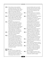
Figure 14.5 Total Q for a quarter-wave resonator on RT/Duroid (
⑀
r
= 2.32), quartz (
⑀
r
= 3.8),
and alumina (
⑀
r
= 10.0) versus substrate thickness.
q
c
= tanh
ͩ
1.043 + 0.121
h′
h
− 1.164
h
h′
ͪ
(14.25c)
Here F(W /h) is given by (14.3). Using the preceding equations, the
characteristic impedance of the shielded microstrip can be calculated from
Z
0
= Z
a
0
/
√
⑀
re
.
For the range of parameters, 1 ≤
⑀
r
≤ 30, 0.05 ≤ W /h ≤ 20, t /h ≤ 0.1,
and 1 < h′/h <∞, the maximum error in Z
0
and
⑀
re
is found to be less than
±1%. When h′/h ≥ 5, the effect of the top cover on the microstrip characteristics
becomes negligible.
The effect of sidewalls on the characteristics of microstrip must also be
included. It is found that the sidewall effect is negligible when S /h ≥ 5, where
443
Microstrip Overview
Figure 14.6 Enclosed microstrip configuration.
S is the separation between the microstrip conductor edge and the sidewall of
the enclosure.
14.2.5 Frequency Range of Operation
The maximum frequency of operation of a microstrip is limited due to several
factors such as excitation of spurious modes, higher losses, pronounced disconti-
nuity effects, low Q due to radiation from discontinuities, effect of dispersion
on pulse distortion, tight fabrication tolerances, handling fragility, and, of course,
technological processes. The frequency at which significant coupling occurs
between the quasi-TEM mode and the lowest order surface wave spurious mode
is given here [1, 3]:
f
T
=
150
h
√
2
⑀
r
− 1
tan
−
1
(
⑀
r
) (14.26)
where f
T
is in gigahertz and h is in millimeters. Thus the maximum thickness
of the quartz substrate (
⑀
r
≅ 3.8) for microstrip circuits designed at 100 GHz
is less than 0.3 mm.
The excitation of higher order modes in a microstrip can be avoided by
operating below the cutoff frequency of the first higher order mode, which is
given approximately by
f
c
≅
300
√
⑀
r
(2W + 0.8h)
(14.27)
where f
c
is in gigahertz, and W and h are in millimeters. This limitation is
mostly applied to low impedance lines that have wide microstrip conductors.
444 Lumped Elements for RF and Microwave Circuits
14.2.6 Power-Handling Capability
The power-handling capacity of a microstrip, like that of any other dielectric
filled transmission line, is limited by heating as a result of ohmic and dielectric
losses and by dielectric breakdown. An increase in temperature due to conductor
and dielectric losses limits the average power of the microstrip line, whereas the
breakdown between the strip conductor and ground plane limits the peak power.
14.2.6.1 Average Power
Microstrip lines are well suited for medium power (about 100 to 200W) applica-
tions and have been extensively used in power MMIC amplifiers. Average power-
handling capability (APHC) of microstrip lines has been discussed in [1, 13–15].
Recent advancements in multilayer microstrip line technologies have made it
possible to realize compact MMICs [16], compact modules [17], low-loss micro-
strip lines [18], and high-Q inductors [19]. In multilayered components, along
with substrate materials, low dielectric constant materials such as polyimide or
BCB are used as a multilayer dielectric. The thermal resistance of polyimide or
BCB is about 200 times the thermal resistance of GaAs or alumina. To ensure
reliable operation of multilayered components such as inductors, capacitors,
crossovers, and inductor transformers for high-power applications, thermal mod-
els are needed for these structures. Bahl [20] discussed the average power-
handling capability of multilayer microstrip lines used in MICs and MMICs.
The APHC of a multilayer microstrip is determined by the temperature
rise of the strip conductor and the supporting dielectric layers and the substrate.
The parameters that play major roles in the calculation of average power capabil-
ity are (1) transmission-line losses, (2) the thermal conductivity of dielectric
layers and the substrate material, (3) the surface area of the strip conductor;
(4) the maximum allowed operating temperature of the microstrip structure,
and (5) ambienttemperature; thatis, thetemperature ofthe mediumsurrounding
the microstrip. Therefore, dielectric layers and substrates with low-loss tangents
and large thermalconductivities will increase the average power-handling capabil-
ity of microstrip lines.
Typically a procedure for APHC calculation consists of the calculation of
conductor and dielectric losses, heat flow due to power dissipation, and the
temperature rise. The temperature rise of the strip conductor can be calculated
from the heat flow field in the microstrip cross section. An analogy between
the heat flow field and the electric field is provided in Table 14.7. The heat
generated by the conductor loss and the dielectric loss is discussed separately
in the following sections. It has been assumed that there are no nonuniformities
in the line and that the line is perfectly matched at two ends.
14.2.6.2 Density of Heat Flow Due to Conductor Loss
A loss of electromagnetic power in the strip conductor generates heat in the
strip. Because of the good heat conductivity of the strip metal, heat generation
445
Microstrip Overview
Table 14.7
Analogy Between Heat Flow and Electric Field
Heat Flow Field Electric Field
1. Temperature, T (°C) Potential, V (V)
2. Temperature gradient, T
g
(°C/m) Electric field, E (V/m)
3. Heat flow rate, Q (W) Flux,
(coulomb)
4. Density of heat flow, q (W/m
2
) Flux density, D (coulomb/m
2
)
5. Thermal conductivity, K (W/m-°C) Permittivity,
⑀
(coulomb/m/V)
6. Density of heat generated,
h
(W/m
3
) Charge density,
(coulomb/m
3
)
7. q =−K ٌTD=−
⑀
ٌV
8. ٌиq =
h
ٌиD =
is uniform along the width of the conductor. Because the ground plane of the
microstrip configuration is held at ambient temperature (i.e., acts as a heat
sink), this heat flows from the strip conductor to the ground plane through
the polyimide layer/layers and the GaAs/alumina substrate. The heat flow can
be calculated by considering the analogous electric field distribution. The heat
flow field in the microstrip structure corresponds to the electrostatic field (with-
out any dispersion) of the microstrip. The electric field lines (and the thermal
field lines in the case of heat flow) spread as they approach the ground plane.
As a first-order approximation, the heat flow from the microstrip conductor
can be considered to follow the rule of 45° thermal spread angle [21] as shown
in Figure 14.7 for a two-layered microstrip configuration. This means that the
heat generated in the microstrip conductor (assuming there are no other heat
sources and heat flow is mainly by conduction) flows down through the dielectric
materials through areas larger than the strip conductor as it approaches the
ground plane, where the ground plane acts as a heat sink. However, to account
accurately for the increase in area normal to heat flow lines, the parallel plate
Figure 14.7 Schematic of microstrip line heat flow based on 45° thermal spread angle rule.
446 Lumped Elements for RF and Microwave Circuits
waveguide model of a microstrip has been used [1, 13]. In the parallel plate
waveguide model of Figure 14.8(c), the capacitance per unit length is the same
as for the multilayer microstrip, Figure 14.8(a), therefore we should have same
electric flux
per unit length of the line. Thus, for a given heat generated, the
heat flow rate will be the same in the two-layer structure of Figure 14.8(a) and
Figure 14.8 (a) Electrical and (b) thermal representation of the two-layer microstrip, and (c)
the equivalent parallel-plate model.
447
Microstrip Overview
in the equivalent parallel plate model of Figure 14.8(c). The equivalent width
of the strip (W
e
) in the parallel plate thermal model is calculated from the
electrical analog and is given by
Z
0
= Z
a
0
/
√
⑀
re
=
120
(d + h)
W
e
(14.28a)
or
W
e
=
120
(h + d )
Z
a
0
(14.28b)
where (h + d ) is the thickness of the dielectric between the plates,
⑀
re
is the
effective dielectric constant of the multilayer medium, and Z
a
0
is the microstrip
impedance with air as the dielectric.
By considering a 1-m-long line and 1-W incident power at the input of
the line, the power available at the end of the line is given by
P = e
−
2
␣
c
(14.29)
The power absorbed (⌬P ) in the line, due to conductor loss in the strip
when 1W of power is incident, is given by
⌬P
c
= 1 − e
−
2
␣
c
(W/m)
or
⌬P
c
= 0.2303
␣
c
(W/m) (14.30)
where
␣
c
(in decibels per meter), the attenuation coefficient due to loss in the
strip conductor, is assumed small. The average density of heat flow q
c
due to
the conductor loss can be written
q
c
=
0.2303
␣
c
W
e
(W/m
2
) (14.31)
14.2.6.3 Density of Heat Flow Due to Dielectric Loss
In addition to the conductor loss, heat is generated by dielectric loss in the
dielectric layers and the supporting substrate. The density of the heat generated
is proportional to the square of the electric field. However, we can consider a
parallel plate model wherein the electric field is uniform and the density of the
448 Lumped Elements for RF and Microwave Circuits
heat generated can also be considered uniform. This assumption ignores the
increased dielectric loss in regions of high electric field near the strip edges.
However, because in most applications the dielectric loss is a small fraction of
the total loss (except for semiconductor substrates like Si or at millimeter-wave
frequencies), the above assumption should hold. The effective width for this
parallel plate waveguide model depends on the spread of electric field lines and
is a function of frequency. Here, as a first-order approximation, no dispersion
is included, and the effective width given in (14.28) can also be used here.
The heat flow in the y-direction caused by a sheet of heat sources due to
dielectric loss can be evaluated by considering the configuration in Figure 14.9.
Here the parallel plate waveguide model is used to calculate the volume for
total heat generated; however, in such calculations, the top conductor is replaced
by an air–dielectric interface. The heat conducted away by air is negligible, and
the air–dielectric boundary can be considered as an insulating wall (correspond-
ing to a magnetic wall in the electric analog). Therefore, the configuration is
modified by removing the insulating wall and incorporating an image source
of heat and an image of the ground plane as shown in Figure 14.9. The space
between the two ground planes is filled by a dielectric media. Now the heat
flow at a point A is obtained by applying the divergence theorem (for heat flow
field) to the volume shown by the dotted lines, that is,
͵͵͵
(ٌиq
d
) dv =
ͶͶ
s
q
d
и ds =
͵͵͵
h
dv (14.32)
where s is the enclosed area, and q
d
and
h
are the density of heat flow due to
dielectric loss and heat generated by the dielectric loss, respectively. The total
q
d
at y = y
1
is contributed by the heat sources lying between y = y
1
and
Figure 14.9 Line geometry for calculating the density of heat flow due to dielectric loss in
a multilayer microstrip.
449
Microstrip Overview
y = h′=h + d (and their images). Note that sources located at y < y
1
(and
their images) do not contribute to the heat flow at y = y
1
. Thus,
q
d
( y) =−(h′−y)
h
(14.33)
The negative sign implies that the heat flow is in the −y-direction (for
y < h′). If ⌬P
d
and
␣
d
(in decibels per meter) are power absorbed and the
attenuation coefficient due to dielectric loss, respectively, the density of heat
generated,
h
, can be written
h
=
⌬P
d
W
e
h′
=
0.2303
␣
d
W
e
h′
(14.34)
This assumes that the heat is being generated uniformly in the parallel
plate waveguide model.
From (14.33) and (14.34)
q
d
( y) =−
0.2303
␣
d
W
e
(1 − y/h′) (14.35)
14.2.6.4 Temperature Rise
The total density of the heat flow due to conductor and dielectric losses can
be expressed in terms of a temperature gradient as
q = q
c
+ q
d
( y) =−K
∂T
∂y
(14.36)
where K is the thermal conductivity of the dielectric media. Therefore, the
temperature at y = h′ (i.e., at the strip conductor) is given by
T = 0.2303
͵
h
′
0
ͭ
␣
c
W
e
K
+
␣
d
W
e
K
(1 − y/h′)
ͮ
dy + T
amb
= 0.2303
΄
͵
h
0
␣
c
W
e
K
g
dy +
͵
h
+
d
h
␣
c
W
e
K
p
dy +
͵
h
0
␣
d
W
e
K
g
ͩ
1 −
y
h + d
ͪ
dy
+
͵
h
+
d
h
␣
d
W
e
K
p
ͩ
1 −
y
h + d
ͪ
dy
΅
+ T
amb
(14.37)
450 Lumped Elements for RF and Microwave Circuits
where T
amb
is the ambient temperature. The corresponding rise in temperature
is
⌬T = T − T
amb
(14.38)
= 0.2303
ͫ
␣
c
ͩ
h
W
e
K
g
+
d
W
e
K
p
ͪ
+
␣
d
ͩ
h(h + 2d )
2W
e
K
g
(h + d )
+
d
2
W
e
K
p
(h + d )
ͪͬ
where K
g
and K
p
are the thermal conductivities of the GaAs substrate and
polyimide layer, respectively. This relation is used for calculating the average
power-handling capability of the microstrip line. Following the procedure dis-
cussed earlier for the two-layered microstrip line, this analysis can be extended
to multilayered microstrip lines.
14.2.6.5 Average Power-Handling Capability
The maximum average power, P
avg
, for a given line can be calculated from
P
avg
= (T
max
− T
amb
)/⌬T (14.39)
where ⌬T denotes rise in temperature per watt and T
max
is the maximum
operating temperature. The maximum operating temperature of microstrip cir-
cuits is limited due to (1) change of substrate properties with temperature, (2)
change of physical dimensions with temperature, and (3) connectors. One can
assume the maximum operating temperature of a microstrip circuit to be the
one at which its electrical and physical characteristics remain unchanged.
The conductor loss consists of two parts: the strip conductor loss and the
ground plane conductor loss. Conductor loss in the ground plane does not
contribute to APHC limitation. However, because the ground plane loss is very
small compared to the strip loss [1], formulas for the total loss could be used
to calculate APHC. The properties of various substrate and conductor materials
[22] are given in Tables 14.8 and Table 14.9, respectively.
For T
max
= 150°C, T
amb
= 25°C, and Z
0
= 50⍀, values of APHC for
various substrates at 10 GHz are calculated and given in Table 14.10. Among
the dielectrics considered, APHC is the lowest for Duroid (0.144 kW) and it
is at a maximum for BeO (52.774 kW). For commonly used alumina (or
sapphire) substrates, a 50⍀ microstrip can carry about 4.63 kW of CW power
at 10 GHz.
Table 14.11 shows the APHC of several multilayer 50-⍀ microstrip lines
on 75-
m-thick GaAs at several frequencies; note that the APHC decreases
with increasing frequency. Lines having characteristic impedances higher than
50⍀ will have lower APHC values as given in Table 14.5 due to higher loss
and narrower line widths.
451
Microstrip Overview
Table 14.8
Properties of Various Dielectric Materials at 10 GHz and 25°C
Dielectric Thermal
Constant, Loss Tangent Conductivity
Material
⑀
r
tan
␦
(× 10
−
4
) K (W/m-؇C)
Alumina (Al
2
O
3
) 9.8 2 37.0
Sapphire 11.7 1 46.0
Quartz 3.8 1 1.0
Si (
= 10
3
⍀-cm) 11.7 >50 145.0
GaAs (
= 10
8
⍀-cm) 12.9 5 46.0
InP 14.0 5 68.0
AlN 8.8 5* 230.0
BeO 6.7* 40 260.0
SiC 40.0 >50 270.0
Polyimide 3.0 10 0.2
Teflon 2.1 5 0.1
Duroid 2.2 9 0.26
Air 1.0 0 0.024
*At 1 MHz.
Table 14.9
Properties of Various Conductor Materials [22]
Thermal
Melting Electrical Expansion Thermal
Point Resistivity Coefficient Conductivity
Metal (؇C) (10
−
6
(⍀-cm) (10
−
6
/؇C) (W/m-؇C)
Copper 1,093 1.7 17.0 393
Silver 960 1.6 19.7 418
Gold 1,063 2.4 14.2 297
Tungsten 3,415 5.5 4.5 200
Molybdenum 2,625 5.2 5.0 146
Platinum 1,774 10.6 9.0 71
Palladium 1,552 10.8 11.0 70
Nickel 1,455 6.8 13.3 92
Chromium 1,900 20.0 6.3 66
Kovar 1,450 50.0 5.3 17
Aluminum 660 4.3 23.0 240
Au–20% Sn 280 16.0 15.9 57
Pb–5% Sn 310 19.0 29.0 63
Cu–W(20% Cu) 1,083 2.5 7.0 248
Cu–Mo(20% Cu) 1,083 2.4 7.2 197
452 Lumped Elements for RF and Microwave Circuits
Table 14.10
Comparison of APHC of 50⍀ Microstrip Lines on Various Substrates at 10 GHz*
Maximum
hW⌬T Average
Substrate
⑀
r
tan
␦
(
m) (
m) (؇C/W) Power (kW)
Duroid 2.2 0.0009 250 760 0.8682 0.144
Si 11.7 0.1540 100 75 0.126 0.992
GaAs 12.9 0.0010 75 50 0.0865 1.445
Al
2
O
3
9.8 0.0002 250 235 0.027 4.630
BeO 6.4 0.0003 250 352 0.00237 52.774
Gold conductors are 4.5
m thick, d = 0, and T
amb
= 25°C.
Table 14.11
Comparison of APHC of 50⍀ Multilayer Microstrip Lines on 75-
m-Thick GaAs*
Polyimide
Maximum Average Power (W)
Thickness
d (
m) 5 GHz 10 GHz 20 GHz 40 GHz
0 2,049 1,445 1,020 720
1 260 181 129 91
3 107 76 53 38
7 71513625
10 63 44 31 22
*Gold conductors are 4.5
m thick except in 3-
m polyimide case, where t = 9
m and
⑀
rd
= 3.2.
Figures 14.10, 14.11, and 14.12 show the variation of APHC as a function
of line width at 5, 10, 20, and 40 GHz for polyimide thicknesses of d = 3, 7,
and 10
m, respectively. As frequency increases from 5 to 40 GHz, the APHC
values decrease by a factor of about 3 due to higher losses; also, as expected,
APHC increases monotonically with line width and decreases with polyimide
thickness.
14.2.6.6 Practical Considerations
The calculations presented above hold good for matched lines. If a transmission
line is not matched to its characteristic impedance, the power distribution
becomes nonuniform along the line due to standing waves that cause nonuniform
heat dissipation. For example, when sections of transmission lines are used in
passive components and matching networks, the APHC of each section will
depend on the standing waves on that line section. The APHC of a long line
453
Microstrip Overview
Figure 14.10 Variation of maximum power-handling capability of multilayer microstrip lines
when the polyimide thickness is 3
m.
Figure 14.11 Variation of maximum power-handling capability of multilayer microstrip lines
when the polyimide thickness is 7
m.
454 Lumped Elements for RF and Microwave Circuits
Figure 14.12 Variation of maximum power-handling capability of multilayer microstrip lines
when the polyimide thickness is 10
m.
is determined at the input point of the line where the RF/microwave signal
enters and the signal is strongest.
Consider a microstrip line of length L and attenuation constant
␣
as
shown in Figure 14.13. If S
i
is the VSWR at the input and S
o
is the VSWR
at the output, they are related by the following relation [23]:
S
i
=
S
o
+ 1 + (S
o
− 1)e
−
2
␣
L
S
o
+ 1 − (S
o
− 1)e
−
2
␣
L
(14.40)
Figure 14.13 A microstrip line section representation.
455
Microstrip Overview
For
␣
L << 1,
S
i
=
S
o
(1 +
␣
L)
1 + S
o
␣
L
(14.41)
The factor (1 +
␣
L)/(1 + S
o
␣
L) is always less than unity, therefore, S
i
is less than S
o
and thus in the worst case S
i
≅ S
o
. The attenuation constant for
the unmatched line,
␣
m
, is given by [23]
␣
m
=
␣
[2(S
2
i
+ 1)/(S
i
+ 1)
2
] (14.42a)
Thus, for the worst-case condition, when the output end of the line is
short circuited or open circuited (S
o
≅∞),
␣
m
becomes
␣
m
= 2
␣
(14.42b)
Therefore, in a worst-case condition, the calculations presented in the
previous section can be derated by a factor 2. Table 14.12 shows derating
coefficient
␥
calculated using (14.42) and increased ambient temperature. This
means that when the line is not matched to its characteristic impedance and
the ambient temperature is greater than 25°C, the calculated APHC values
should be reduced by
␥
factor.
If the case temperature is about 60°C and the circuits have short-circuited
lines, the derating factor for such lines is about 2.78. This means that at 10
Table 14.12
APHC Derating Coefficient
␥
Calculated as a Function of VSWR
at Various Ambient Temperatures
VSWR T
amb
= 25؇C T
amb
= 60؇C T
amb
= 80؇C
1 1.00 1.39 1.79
2 1.11 1.54 1.98
3 1.25 1.74 2.23
4 1.36 1.89 2.43
5 1.44 2.00 2.57
6 1.51 2.10 2.70
7 1.56 2.17 2.79
8 1.61 2.24 2.88
9 1.64 2.28 2.93
10 1.67 2.32 2.98
20 1.82 2.53 3.25
∞ 2.00 2.78 3.57
456 Lumped Elements for RF and Microwave Circuits
GHz, the maximum average power-handling values of a 30-
m-wide multilayer
microstrip lines are 312, 13.9, 6.9, and 5.8W for polyimide thicknesses of 0,
3, 7, and 10
m, respectively.
14.2.6.7 Peak Power-Handling Capability
The calculation of peak power-handling capability of microstrip lines is more
complicated. The peak voltage that can be applied without causing dielectric
breakdown determines the peak power-handling capability (PPHC) of the micro-
strip. If Z
0
is the characteristic impedance of the microstrip and V
0
is the
maximum voltage the line can withstand, the maximum peak power is given
by
P
p
=
V
2
0
2Z
0
(14.43)
Thick substrates can support higher voltages (for the same breakdown
field). Therefore, low impedance lines and lines on thick substrates have higher
PPHC.
The sharp edges of a strip conductor serve as field concentrators. The
electric field tends to a large value at the sharp edges of the conductor if it is
a flat strip and decreases as the edge of the conductor is rounded off more and
more. Therefore, thick and rounded strip conductors will increase breakdown
voltage.
The dielectric strengths of the substrate material as well as of the air play
important roles. The breakdown strength of dry air is approximately 30 kV/cm.
Thus the maximum (tangential) electric field near the strip edge should be less
than 30 kV/cm. To avoid air breakdown near the strip edge, the edge of the
strip conductor can be painted with a dielectric paint that has the same dielectric
constant as that of the substrate and is lossless or by using an overlay of silicon
rubber as discussed in Section 7.2.5. An additional factor, which may reduce
PPHC, is the effect of internal mismatches.
14.3 Coupled Microstrip Lines
Inductors and transformers can be analyzed using coupled microstrip line theory.
The theory of such structures has been treated in a recently published book [22].
Coupled microstrip structures are characterized by characteristic impedances (or
admittances) and phase velocities (or effective dielectric constants) for the two
modes known as even and odd. Design equations given later for coupled lines
relate mode impedances and effective dielectric constants to the coupled line
geometry, that is, strip width, spacing S between the strips, dielectric thickness
457
Microstrip Overview
h, and dielectric constant
⑀
r
. One can write design equations for these characteris-
tics directly in terms of static capacitances for the coupled line geometry. Even-
and odd-mode capacitances for the symmetric two-conductor coupled lines
shown in Figure 14.14 are obtained first.
14.3.1 Even-Mode Capacitance
As shown in Figure 14.14(a), the even-mode capacitance C
e
can be divided
into three capacitances:
C
e
= C
p
+ C
f
+ C
f
′
(14.44)
where C
p
denotes the parallel plate capacitance between the strip and the ground
plane, and C
f
is the fringe capacitance at the outer edge of the strip. It is the
Figure 14.14 Analysis of coupled microstrip lines in terms of capacitances: (a) even-mode
capacitance and (b) odd-mode capacitance.
458 Lumped Elements for RF and Microwave Circuits
fringe capacitance of a single microstrip line and can be evaluated from the
capacitance of the microstrip line and the value of C
p
. The term C
f
′
accounts
for the modification of fringe capacitance C
f
of a single line due to the presence
of another line. Expressions for C
p
, C
f
, and C
f
′
are given here [1, 24]:
C =
⑀
0
⑀
r
W /h (14.45a)
2C
f
=
√
⑀
re
/(cZ
0
) −
⑀
0
⑀
r
W /h (14.45b)
and
C
f
′
=
C
f
1 + A(h/S ) tanh (10S /h )
ͩ
⑀
r
⑀
re
ͪ
1/4
(14.45c)
where
A = exp [−0.1 exp (2.33 − 1.5W /h)] (14.45d)
The capacitances obtained by using the preceding design equations were
compared with those obtained from [25]. The values are found to be accurate
to within 3% over the following range of parameters:
0.1 ≤ W /h ≤ 10 0.1 ≤ S /h ≤ 51≤
⑀
r
≤ 18
14.3.2 Odd-Mode Capacitance
Odd-mode capacitance C
o
can be decomposed into four constituents: C
f
, C
p
,
C
gd
, and C
ga
as shown in Figure 14.14(b); that is,
C
o
= C
f
+ C
p
+ C
gd
+ C
ga
(14.46)
Expressions for C
f
and C
p
are the same as those given earlier in the case
of C
e
. Capacitance C
ga
describes the gap capacitance in air. Its value can be
obtained from the capacitance of a slotline of width W with air as dielectric as
given below:
C
ga
=
⑀
0
K (k′)
K (k)
, k =
S
S + 2W
, and k′=
√
1 − k
2
(14.47a)
where K (k) and K (k′) denote the elliptic function and its complement. Use
of simplified expressions for K (k′)/K (k) yields the following value for C
ga
:
459
Microstrip Overview
C
ga
=
Ά
⑀
0
ln
ͭ
2
1 +
√
k′
1 −
√
k′
ͮ
for 0 ≤ k
2
≤ 0.5
⑀
0
/ln
ͭ
2
1 +
√
k
1 −
√
k
ͮ
for 0.5 ≤ k
2
≤ 1
(14.47b)
The last term C
gd
represents the capacitance value due to the electric flux
in the dielectric region and its value is evaluated as follows:
C
gd
=
⑀
0
⑀
r
ln coth
ͩ
S
4h
ͪ
+ 0.65C
f
ͭ
0.02
S /h
√
⑀
r
+
ͩ
1 −
1
⑀
2
r
ͪͮ
(14.48)
The first term in (14.48) is obtained from coupled stripline geometry.
The second term represents its modification for coupled microstrip.
14.3.3 Characteristic Impedances
Characteristic impedances Z
0e
and Z
0o
can be obtained by using the following
relationships:
Z
0e
=
ͫ
c
√
C
a
e
C
e
ͬ
−
1
(14.49a)
Z
0o
=
ͫ
c
√
C
a
o
C
o
ͬ
−
1
(14.49b)
where C
a
e
and C
a
o
are even- and odd-mode capacitances for the coupled micro-
strip configuration with air as the dielectric.
The values of impedances obtained by using the preceding design equations
have an error of less than 3% for the parameters lying in the range
⑀
r
≤ 18,
0.1 ≤ W /h ≤ 2, and 0.05 ≤ S /h ≤ 2.
14.3.4 Effective Dielectric Constants
Effective dielectric constants
⑀
ree
and
⑀
reo
for even and odd modes, respectively,
can be obtained from C
e
and C
o
by these relations:
⑀
ree
= C
e
/C
a
e
(14.50a)
⑀
reo
= C
o
/C
a
o
(14.50b)
460 Lumped Elements for RF and Microwave Circuits
More accurate values of capacitances can be obtained from the closed-
form expressions reported by Kirschning and Jansen [25].
14.4 Microstrip Discontinuities
Various types of discontinuities that occur in the conductor of planar transmis-
sion lines, such as microstrips, are shown in Figure 14.15. Examples of circuits
Figure 14.15 Typical planar strip transmission-line discontinuities.
461
Microstrip Overview
and circuit elements, wherein these discontinuities are frequently encountered,
are also shown in this figure.
A complete understanding of the design of MICs requires characterization
of the discontinuities present in these circuits. Approximate closed-form expres-
sions for various discontinuity elements are given in [1].
14.5 Compensated Microstrip Discontinuities
In MIC designs, microstrip discontinuities should either be taken into account
or microstrip structures with compensated discontinuities should be used. In
general, compensated discontinuities improve circuit performance and the band-
width. Usually chamfered bends or rounded corners are used in MICs and
MMICs. The chamfered discontinuity technique is also known as discontinuity
compensation in which the discontinuity reactances are minimized by removing
appropriate portions of the microstrip conductor near the discontinuity location.
In this section, we describe briefly the step-in-width, right-angled bend, and
T-junction compensated microstrip discontinuities.
14.5.1 Step-in-Width
Compensation of a step discontinuity has been reported [1, 26–31] using
appropriate tapers. In this case the effect of discontinuity reactances is reduced
by chamfering the large width. The taper length depends on the step ratio,
dielectric constant value, and the substrate thickness h. For h/
≤ 0.01 and a
step ratio of less than 3, the step discontinuity reactance is negligible and
generally no compensation technique is needed. Figure 14.16 shows three types
of tapers. The taper shown in Figure 14.16(a) has been studied using a planar
waveguide model, which was described in Section 14.2.6. For a gradual taper,
shown in Figure 14.16(b), closed-form expressions for the contour of a taper
compensating step discontinuity in microstrip lines is given by Raicu [29]. For
Figure 14.16 Three different kinds of compensated step-in-width discontinuity configurations:
(a) linear taper, (b) curved taper, and (c) partial linear taper.
462 Lumped Elements for RF and Microwave Circuits
a partial taper, shown in Figure 14.16(c), discontinuity compensation on the
75- to 125-
m-thick GaAs substrate using a commercial full-wave analysis
CAD tool was performed. For a step width ratio ranging from 3 to 13, the
step discontinuity reactance is negligible when L = W
1
/8 and W
1
′=0.33W
1
.
14.5.2 Chamfered Bend
Data on the optimum amount of chamfering in a microstrip bend have been
given in [30] as follows:
M = 52 + 65 exp (−1.35W /h) (14.51)
for W /h ≥ 0.25 and
⑀
r
≤ 25, where M is the percentage chamfer given by
(X /d ) × 100% with X and d shown in Figure 14.17. For a chamfered bend,
the reflection coefficient S
11
∼ 0, when the transmission line is terminated
by an impedance equal to its characteristic impedance, but the discontinuity
reactances cause a reduction ⌬b in length compared to that measured along
the centerlines of the microstrip lines. A closed-form expression for this reduction
in length can be written [31]
⌬b/D = 0.16{2 − ( f /f
p
)
2
} (14.52)
where D and f
p
are given by
D = 120
h/
√
⑀
re
Z
0
f
p
= 0.4Z
0
/h
where f
p
and h are in gigahertz and millimeters, respectively.
Figure 14.17 Geometry of a chamfered bend.
463
Microstrip Overview
Several other types of chamfering, as shown in Figure 14.18, have been
studied and optimum chamfer dimensions are also given. Figure 14.19 compares
calculated S
11
for uncompensated right-angled bend discontinuity with compen-
sated topologies. We note that the configuration shown in Figure 14.18(c)
provides the best compensation for this example.
14.5.3 T-Junction
T-junction discontinuity compensation is much more difficult than the step-in-
width and right-angled bend discontinuity compensation techniques described in
previous subsections.Figure 14.20(a) shows T-junction compensation configura-
Figure 14.18 (a–f ) Six different configurations for compensated right-angled bends.
464 Lumped Elements for RF and Microwave Circuits
Figure 14.19 Magnitude of the reflection coefficient as a function of frequency for several
compensated and uncompensated right-angled bends: W = 73
m, h = 100
m,
⑀
r
= 12.9, and the curved line has a mean radius = 220.
Figure 14.20 (a) T-junction discontinuity compensation configurations and (b) minimized
T-junction discontinuity effect configuration.
465
Microstrip Overview
tions using rectangular and triangular notches and their approximate dimensions
for h/
<< 1. However, accurate compensation depends on line widths, dielectric
constant, and the substrate thickness. Figure 14.20(b) illustrates T-junction
discontinuity minimization configurations in which the line widths are tapered
to minimize the junction effect. In this case the taper length is about twice the
line width or substrate thickness whichever is larger, and the tapered length
becomes a part of the design parameter.
References
[1] Gupta, K. C., et al., Microstrip Lines and Slotlines, 2nd ed., Norwood, MA: Artech House,
1996.
[2] Wheeler, H. A., ‘‘Transmission Line Properties of Parallel Strips Separated by a Dielectric
Sheet,’’ IEEE Trans. Microwave Theory Tech., Vol. MTT-13, March 1965, pp. 172–185;
see also Wheeler, H. A., ‘‘Transmission Line Properties of a Strip on a Dielectric Sheet
on a Plane,’’ IEEE Trans. Microwave Theory Tech., Vol. MTT-25, August 1977,
pp. 631–647.
[3] Vendelin, G. D., ‘‘Limitations on Stripline Q,’’ Microwave J., Vol. 13, May 1970,
pp. 63–69.
[4] Hammerstad, E. O., ‘‘Equations for Microstrip Circuit Design,’’ Proc. European Microwave
Conf., 1975, pp. 268–272.
[5] Bahl, I. J., and D. K. Trivedi, ‘‘A Designer’s Guide to Microstrip Line,’’ Microwaves,
Vol. 16, May 1977, pp. 174–182.
[6] Bahl, I. J., ‘‘Easy and Exact Methods for Shielded Microstrip Design,’’ Microwaves,
Vol. 17, December 1978, pp. 61–62.
[7] Bahl, I. J., and K. C. Gupta, ‘‘Average Power Handling Capability of Microstrip Lines,’’
IEEE J. Microwaves, Optics and Acoustics, Vol. 3, January 1979, pp. 1–4.
[8] Garg R., ‘‘Microstrip Design Guides,’’ Int. J. Electronics, Vol. 46, 1979, pp. 187–192.
[9] Denlinger, E. J., ‘‘Losses in Microstrip Lines,’’ IEEE Trans. Microwave Theory Tech.,
Vol. MTT-28, June 1980, pp. 513–522.
[10] Hammerstad, E., and O. Jensen, ‘‘Accurate Models for Microstrip Computer-Aided
Design,’’ IEEE MTT-S Int. Microwave Symp. Dig., 1980, pp. 407–409.
[11] March, S. L., ‘‘Empirical Formulas for the Impedance and Effective Dielectric Constant
of Covered Microstrip for Use in the Computer-Aided Design of Microwave Integrated
Circuits,’’ Proc. European Microwave Conf., Kent, England: Microwave Exhibitors &
Publishers Ltd., 1981, pp. 671–676.
[12] Kobayashi, M., ‘‘A Dispersion Formula Satisfying Recent Requirements in Microstrip
CAD,’’ IEEE Trans. Microwave Theory Tech., Vol. MTT-36, August 1988, pp. 1246–1250.
[13] Bahl, I. J., and K. C. Gupta, ‘‘Average Power-Handling Capability of Microstrip Lines,’’
IEEE J. Microwaves, Optics and Acoustics, Vol. 3, January 1979, pp. 1–4.
466 Lumped Elements for RF and Microwave Circuits
[14] Sturdivant, R., and T. Theisen, ‘‘Heat Dissipating Transmission Lines,’’ Applied Microwave
and Wireless, Vol. 7, Spring 1995, pp. 57–63.
[15] Parnes, M., ‘‘The Correlation Between Thermal Resistance and Characteristic Impedance
of Microwave Transmission Lines,’’ Microwave J., Vol. 43, March 2000, pp. 82–94.
[16] Toyoda, I., T. Tokumitsu, and M. Aikawa, ‘‘Highly Integrated Three-Dimensional MMIC
Single-Chip Receiver and Transmitter,’’ IEEE Trans. Microwave Theory Tech., Vol. 44,
December 1996, pp. 2340–2346.
[17] Nakatsugawa, M., et al., ‘‘Line-Loss and Size Reduction Techniques for Millimeter-Wave
RF Front-End Boards by Using a Polyimide/Alumina-Ceramic Multilayer Configuration,’’
IEEE Trans. Microwave Theory Tech., Vol. 45, December 1997, pp. 2308–2315.
[18] Bahl, I. J., et al., ‘‘Low Loss Multilayer Microstrip Line for Monolithic Microwave Inte-
grated Circuits Applications,’’ Int. J. RF and Microwave Computer-Aided Engineering,
Vol. 8, November 1998, pp. 441–454.
[19] Bahl, I. J., ‘‘High Current Capacity Multilayer Inductors for RF and Microwave Circuits,’’
Int. J. RF and Microwave Computer-Aided Engineering, Vol. 10, March 2000, pp. 139–146.
[20] Bahl, I. J., ‘‘Average Power Handling Capability of Multilayer Microstrip Lines,’’ Int. J.
RF and Microwave Computer-Aided Engineering, Vol. 11, November 2001, pp. 385–395.
[21] Masana, F. N., ‘‘A Closed Form Solution of Junction of Substrate Thermal Resistance in
Semiconductor Chips,’’ IEEE Trans. Components, Packaging, and Manufacturing Tech. Part
A, Vol. 19, December 1996, pp. 539–545.
[22] Mongia, R., I. Bahl, and P. Bhartia, RF and Microwave Coupled-Line Circuits, Norwood,
MA: Artech House, 1999, pp. 499–500.
[23] Fuks, R., ‘‘Compute Power Rating for Unmatched Lines,’’ Microwaves and RF, Vol. 37,
October 1998, pp. 100–112.
[24] Garg, R., and I. J. Bahl, ‘‘Characteristics of Coupled Microstrip Lines,’’ IEEE Trans.
Microwave Theory Tech., Vol. MTT-27, 1979, pp. 700–705; see also Corrections, IEEE
Trans. Microwave Theory Tech., Vol. MTT-28, 1980, p. 272.
[25] Kirschning, M., and R. H. Jansen, ‘‘Accurate Wide-Range Design Equations for Parallel
Coupled Microstrip Lines,’’ IEEE Trans. Microwave Theory Tech., Vol. MTT-32, 1984,
pp. 83–90; see also Corrections, IEEE Trans. Microwave Theory Tech., Vol. MTT-33,
1985, p. 288.
[26] Malherbe, J. A. G., ‘‘The Compensation of Step Discontinuities in TEM-Mode Trans-
mission Lines,’’ IEEE Trans. Microwave Theory Tech., Vol. MTT-26, November 1978,
pp. 883–885.
[27] Chadha, R., and K. C. Gupta, ‘‘Compensation of Discontinuities in Planar Transmission
Lines,’’ IEEE Trans. Microwave Theory Tech., Vol. MTT-30, December 1982,
pp. 2151–2156.
[28] Hoefer, W. J. R., ‘‘A Contour Formula for Compensated Microstrip Steps and Open
Ends,’’ IEEE MTT-S Int. Microwave Symp. Dig., Boston, MA, 1983, pp. 524–526.
[29] Raicu, D., ‘‘Universal Taper for Compensation of Step Discontinuities in Microstrip
Lines,’’ IEEE Microwave Guided Lett., Vol. 1, September 1991, pp. 249–251.