Microwave Ring Circuits and Related Structures phần 10 pps
Bạn đang xem bản rút gọn của tài liệu. Xem và tải ngay bản đầy đủ của tài liệu tại đây (500.04 KB, 38 trang )
The single-balanced mixer consists of two diodes arranged so that the local
oscillator (LO) pump is 180° out of phase and the radio frequency (RF) signal
is in phase at the diodes, or vice versa. The balanced operation results in LO
noise suppression and provides a larger dynamic range and better inter-
modulation suppression compared with the single-ended mixer [1]. Figure 12.2
shows a rat-race hybrid-ring mixer. It consists of a hybridring coupler, two dc
blocks, two mixer diodes, two RF chokes, and a low-pass filter. The RF input
is split equally into two mixer diodes. The LO input is also split equally but is
180° out of phase at the mixer diodes. Both the LO and RF are mixed in these
diodes, which generate signals that are then combined through the ring and
taken out through a low-pass filter.The LO and RF ports are isolated.The RF
chokes provide a tuning mechanism and prevent the RF signal from leaking
into ground.
Because the microstrip hybrid ring coupler is bandwidth limited, only a
10 to 20% bandwidth has been achieved using rat-race mixers. Rat-race
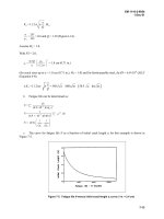
mixers have been demonstrated up to 94 GHz. Figure 12.3 shows the circuit
of a 94-GHz rat-race mixer. A conversion loss of less than 8 dB was achieved
over a 3-GHz RF bandwidth using LO pump power of +8 dBm, and less
than 6.5 dB with LO pump power of +10 dBm [2]. The results are given in
Figure 12.4. Wide-band mixers can be constructed using the broadband copla-
nar waveguide hybrid-ring couplers and magic-Ts described in Chapters 8
and 9.
RAT-RACE BALANCED MIXERS 331
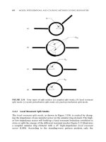
FIGURE 12.1 Physical layout of the microstrip rat-race hybrid-ring coupler.
332 RING MIXERS, OSCILLATORS, AND OTHER APPLICATIONS
FIGURE 12.2 Rat-race mixer configuration.
FIGURE 12.3 94-GHz rat-race mixer [2]. (Permission from IEEE.)
12.3 SLOTLINE RING QUASI-OPTICAL MIXERS
The slotline ring antenna discussed in Chapter 11 was used to build a quasi-
optical mixer [3]. Figure 12.5 shows the circuit arrangement. The RF signal
arrives as a horizontally polarized plane wave incident perpendicular to the
antenna. The LO signal is vertically polarized, and can arrive from either side
of the structure. V
LO
and V
RF
are the electric field vectors on the antenna plane.
By resolving each vector into two perpendicular components, it is easy to see
that the mixer diode D
1
receives
while D
2
receives
In effect, each diode has its own independent mixer circuit, with the inter-
mediate frequency (IF) outputs added in parallel. The IF signal appears as a
voltage between the central metal disk and the surrounding ground plane, and
VV
LO RF
2
+
VV
LO RF
2
-
SLOTLINE RING QUASI-OPTICAL MIXERS 333
FIGURE 12.4 Performance of a 94-GHz rat-race mixer [2]. (Permission from IEEE.)
is removed through an RF choke. A double-balanced mixer with improved
isolation can be made by adding two additional diodes D
3
and D
4
, as indicated.
The antenna-mixer has good LO-to-RF isolation, because of the symmetry
provided by the balanced configuration.A conversion loss of 6.5 dB was meas-
ured for this quasi-optical mixer operating at X-band [3]. Similar circuits were
recently analyzed using a nonlinear analysis [4].
12.4 RING OSCILLATORS
Since a ring circuit is a resonator, it can be used to stabilize an oscillator. Figure
12.6 shows a high-temperature superconductor ring-stabilized FET oscillator
built on LaAlO
3
substrate [5]. The circuit exhibited an output power of
11.5 dBm and a maximum efficiency of 11.7%. At 77 K, the best phase noise
of the superconductor oscillator was -68 dBc/Hz at an offset frequency of 10
kHz. This phase noise level is 12 dB and 26 dB less than the copper oscillator
at 77 K and 300 K, respectively. A similar circuit was demonstrated using a
high-electron mobility transistor (HEMT) device giving a phase noise of
-75 dBc/Hz at 10 kHz from the carrier [6].
A voltage-tuned microstrip ring-resonator oscillator was reported to have
a tuning bandwidth of 30% [7]. The circuit employed two microwave mono-
lithic integrated circuit (MMIC) amplifiers as the active devices, and a tunable
microstrip ring resonator in the feedback path was designed to operate over
the frequency range of 1.5–2.0 GHz and fabricated with all the components
mounted inside the ring as shown in Figure 12.7. A varactor diode was
334 RING MIXERS, OSCILLATORS, AND OTHER APPLICATIONS
FIGURE 12.5 Antenna-mixer configuration [3]. (Permission from IEEE.)
RING OSCILLATORS 335
FIGURE 12.6 The physical layout of the reflection-mode oscillator on a 1-cm
2
LaAlO
3
substrate [5]. (Permission from IEEE.)
FIGURE 12.7 Layout of the microstrip ring resonator oscillator [7]. (Permission from
Electronics Letters.)
336 RING MIXERS, OSCILLATORS, AND OTHER APPLICATIONS
FIGURE 12.8 Oscillation frequency vs. tuning voltage [7]. (Permission from Elec-
tronics Letters.)
mounted across the gap in the ring. By adjusting the bias voltage to the var-
actor, the resonant frequency of the ring was varied and the oscillation fre-
quency was thus tuned. Figure 12.8 shows the oscillation frequency as a
function of tuning varactor voltage, and Figure 12.9 shows the output power.
The frequency was adjusted from 1.533 to 1.92 GHz with the capacitance
changed from 0.44 to 3.69 pF. The oscillation frequency can be tuned down to
1.44 GHz, corresponding to a tuning range of 28.8% by slightly forward
biasing the diode with 1-mA current [7].
Dual-mode ring resonators were used to build low phase noise voltage-
controlled oscillators (VCOs) and oscipliers (oscillator plus multiplier) [8].
Figure 12.10 shows the VCO circuit configuration. Circuit 1 covers the lower
frequency band ranges, while circuit 2 covers the higher frequency band
ranges. Both oscillators are composed of a common dual-mode resonator and
two identical negative resistance circuits. Using a dual-mode resonator reduces
the variable frequency range to about one-half of the conventional one.
As a result, the phase noise of the oscillators are significantly improved.
Figure 12.11 shows the circuit configuration of osciplier [8]. The dual-mode
resonator can be used to obtain two outputs of the fundamental frequency
f
o
and its second harmonic frequency 2f
o
, separately, with high isola-
tion between them. An osciplier with an output signal of 1.6 GHz was
demonstrated with a fundamental suppression level of 18 dB [8].
RING OSCILLATORS 337
FIGURE 12.9 Output power vs. oscillation frequency [7]. (Permission from Electron-
ics Letters.)
FIGURE 12.10 Circuit configuration of a low phase noise VCO [8]. (Permission from
IEEE.)
338 RING MIXERS, OSCILLATORS, AND OTHER APPLICATIONS
V
g
V
d
GND
Output
GD
S
l
3
l
4
l
5
l
6
l
7
l
8
l
9
FIGURE 12.12 Feedback ring resonator oscillator [9]. (Permission from IEEE.)
Another type ring oscillator using feedback configuration is shown in
Figure 12.12. This configuration consists of a feedback ring circuit and a two-
port negative-resistance oscillator with input and output matching networks
[9]. The close-loop ring resonator using a pair of orthogonal feed lines sup-
presses odd resonant frequencies and operates at even resonant frequencies.
This operation has a similar characteristic of high operating resonant
frequencies as that of the push-push oscillators [10, 11]. Also, the high Q ring
resonator is used to reduce the noise of the two-port negative-resistance oscil-
lator.
To investigate the high-frequency operation of the ring circuit, an orthog-
onal feed ring resonator is shown in Figure 12.13. As seen in Figure 12.13, the
closed-loop ring resonator with total length of l = nl
g
is fed by two orthogo-
nal feed lines, where n is the mode number and l
g
is the guided-wavelength.
The ring resonator fed by the input and output feed lines represents a shunt
circuit, which consists of the upper and lower sections of l
1
= 3nl
g
/4 and l
2
=
FIGURE 12.11 Circuit configuration of an osciplier [8]. (Permission from IEEE.)
nl
g
/4, respectively. The ABCD matrixes of the upper and lower sections of the
lossless ring circuit are given by
(12.1a)
and
(12.1b)
where b is the propagation constant and Z
o
= 1/Y
o
is the characteristic imped-
ance of the ring resonator. The Y parameters of the upper and lower sections
are obtained from (12.1a) and (12.1b) and given by
(12.2)
where j = upper or lower is for upper or lower sections. In addition, the total
Y parameter of the whole circuit is expressed as
(12.3)
Furthermore, S
21
of the ring circuit can be found from (12.3) and is expressed
as
Y
Y
Y
Y
Y
Y
Y
Y
Y
Y
Y
Y
jY l l
jY l l
jY l l
jY l l
upper lower
o
o
o
o
11
21
12
22
11
21
12
22
11
21
12
22
12
12
12
12
È
Î
Í
˘
˚
˙
=
È
Î
Í
˘
˚
˙
+
È
Î
Í
˘
˚
˙
=
-+
()
+
()
È
Î
Í
+
()
-+
(
)
cos cot
csc csc
csc csc
cos cot
bb
bb
bb
bb
Y
Y
Y
Y
DB
B
BC AD B
AB
j
jj
j
jj jj j
jj
11
21
12
22
1
È
Î
Í
˘
˚
˙
=
-
È
Î
Í
-
()
˘
˚
˙
/
/
/
/
A
C
B
D
l
jY l
jZ l
l
lower
o
o
È
Î
Í
˘
˚
˙
=
È
Î
Í
˘
˚
˙
cos
sin
sin
cos
b
b
b
b
2
2
2
2
A
C
B
D
l
jY l
jZ l
l
upper
o
o
È
Î
Í
˘
˚
˙
=
È
Î
Í
˘
˚
˙
cos
sin
sin
cos
b
b
b
b
1
1
1
1
RING OSCILLATORS 339
Input
Output
1
l
2
l
12
g
ll l n
l
=+=
FIGURE 12.13 Configuration of the ring resonator fed by two orthogonal feed lines
[9]. (Permission from IEEE.)
(12.4)
For odd-mode excitation
(12.5a)
and for even-mode excitation
(12.5b)
The calculated results in (12.5) show that the ring resonator fed by two
orthogonal fed lines can suppress the odd mode resonant frequencies and
operate at even mode resonant frequencies only. This operation has a similar
characteristic of high operating resonant frequencies as that of the push-push
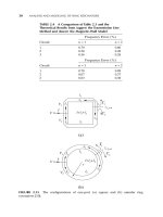
oscillator [10, 11]. Figure 12.14 shows the layout of the ring circuit using two
orthogonal feed lines with coupling gap size of s.This ring circuit was designed
at the fundamental mode of 6 GHz and fabricated on a 20-mil-thick
RT/Duroid 5870 substrate with a relative dielectric constant of e
r
= 2.33.
The dimensions of the ring circuit are l
1
= 27.38 mm, l
2
= 9.13 mm, l
f
= 8 mm,
w = 1.49 mm, and s = 0.2 mm.
The measured and simulated results of this circuit are shown in Figure
12.15. The simulation is performed using an IE3D EM simulator [12]. Observ-
ing the measured and simulated results, they agree well with each other. The
results also agree with the predictions given by (12.5).The measured unloaded
Q of the ring resonator is 125.2.
Sn
21
1246==, , , .
Sn
21
0135==, , , .
S
YY
YYY YYY
j
nn
j
nn nn
o
oo
21
21
11 22 12 21
2
2
2
2
3
22
1
3
22
3
22
=
-
+
()
+
()
-
=
-+
Ê
Ë
ˆ
¯
-+
Ê
Ë
ˆ
¯
È
Î
Í
˘
˚
˙
++
È
Î
Í
˘
˚
˙
csc csc
cot cot csc csc
pp
pp pp
340 RING MIXERS, OSCILLATORS, AND OTHER APPLICATIONS
Input
Output
1
l
2
l
f
l
s
w
w
FIGURE 12.14 Configuration of the ring resonator using enhanced orthogonal feed
lines [9]. (Permission from IEEE.)
By using the characteristic of the high resonant frequency operation shown
in Figure 12.15, the feedback oscillator shown in Figure 12.12 can oscillate at
high oscillation frequency. The active device used in the oscillator is a NE
32484A HEMT. The dimensions of the oscillator are l
3
= 3 mm, l
4
= 6.95 mm,
l
5
= 15.19 mm, l
6
= 10.69 mm, l
7
= 7.3 mm, l
8
= 9.47 mm, and l
9
= 21.19 mm. The
two-port negative-resistance oscillator uses the one-open-end S terminal as a
series-feedback element to obtain a potential instability. Also, with the input
and output matching network, the two-port oscillator with an applied bias of
of V
gs
=-0.65 V and V
ds
= 1 V has a negative resistance around 12 GHz.
Inspecting the equation of the DC-to-RF efficiency in Equation (12.6), if the
decreasing rate of I
ds
V
ds
is faster than that of the RF output power, P
out
, then
oscillators can possibly research to a high DC-to-RF efficiency.
(12.6)
Observing Equation (12.6), the maximum efficiency can be obtained by select-
ing a low V
gs
and V
ds
. The highest DC-to-RF efficiency of the oscillator of
41.4% is obtained with output power of 6.17 dBm at the oscillation frequency
of 12.104 GHz.
Figure 12.16 shows the measured spectrum of the oscillator with applied
voltages of V
gs
=-0.65 V and V
ds
= 1 V. Also, as shown in Figure 12.16, the
oscillator is operated at the second harmonic of the ring resonator. The oscil-
lator has the efficiency of 48.7% with output power of 3.41 mW at 12.09 GHz.
The phase noise of the oscillator is -96.17 dBc/Hz at offset frequency of
100 KHz. The second and third harmonics of the oscillator are 22.8 dB and
15.1 dB down from the fundamental oscillation frequency.
Efficiency =
()
=¥h %%
P
IV
out
ds ds
100
RING OSCILLATORS 341
Magnitude S
21
(dB)
n=1
n=2
n=4
n=3
Measurement
Simulation
0 5 10 15 20 25 30
Frequency (GHz)
-50
-40
-30
-20
-10
0
FIGURE 12.15 Simulated and measured results for the ring resonator using enhanced
orthogonal feed lines [9]. (Permission from IEEE.)
These harmonics have less effect on the fundamental oscillation frequency.
Comparing with other oscillators [13], this oscillator provides a high DC-to-
RF efficiency.
Figure 12.17 shows the configuration of the ring resonator oscillator inte-
grated with a piezoelectric transducer (PET) with an attached dielectric per-
turber. When applying a DC voltage to the PET, the PET move the perturber
up or down vertically to change the effective dielectric constant of the ring
resonator [9, 14], and thus vary the resonant frequency of the ring resonator.
Figure 12.18 shows the measured results of the oscillator using the PET
tuning.The perturber attached on the PET has a dielectric constant of e
r
= 10.8
and a thickness of h = 50 mil. The tuning range of the oscillator is from
11.49 GHz (+90 V) with a power output of 3.17 dBm to 12 GHz (0 V) with a
power output of 5.33 dBm.
Figure 12.19 shows the tunable oscillation frequencies and output power
levels versus PET tuning voltages. As seen in Figure 12.19, the PET tuning
range is about 4.25% around the oscillation frequency of 12 GHz, and the
output power is varied from 2.67 to 5.33 dBm. This good tuning rage is due to
a large area perturbation on the whole ring that significantly tunes the reso-
nant frequency of the ring. In addition, by using a higher dielectric perturber,
a wider tuning range and a lower DC applied voltage could be achieved [15].
12.5 MICROWAVE OPTOELECTRONICS APPLICATIONS
An optical control in microwave ring devices has been developed for its poten-
tial applications in signal switching, mixing, and frequency modulation. Fur-
342 RING MIXERS, OSCILLATORS, AND OTHER APPLICATIONS
10
20
0
30
-10
-20
-30
-40
-50
-60
-70
12.0912.07
12.05
12.0312.01
12.19
12.17
12.1512.1312.11
11.99
Output Power (dBm)
Frequency (GHz)
FIGURE 12.16 Output power for the feedback ring resonator oscillator operated at
the second harmonic of the ring resonator [9]. (Permission from IEEE.)
MICROWAVE OPTOELECTRONICS APPLICATIONS 343
Dielectric
perturber
V
dc
V
g
V
d
GND
Output
PET
(a)
Perturber
V
dc
Oscillator
PE
T
T
e
s
t
f
i
x
t
u
r
e
(b)
FIGURE 12.17 Configuration of the tunable oscillator using a PET: (a) top view and
(b) 3D view [9]. (Permission from IEEE.)
thermore, microwave-optoelectronic mixers fabricated on GaAs substrate
have been reported [16–19]. The layout of the circuit is illustrated in Figure
12.20. Since the Q-factor of the ring resonator is better than that of the linear
resonator, the ring was chosen for experiments. The circuit is fabricated on
semi-insulating GaAs.
Resonances were measured to occur at 3.467 GHz, 7.18 GHz, and
10.4 GHz. Corresponding loaded Q-factors are 45, 58, and 74. Two 4-mm slits
are introduced at diametrically opposite locations of the ring for optical exci-
tation. These slits are designed to be collinear with the feed lines so that mode
344 RING MIXERS, OSCILLATORS, AND OTHER APPLICATIONS
10
20
0
30
-10
-20
-30
-40
-50
-60
-70
11.7511.68
11.61
11.5411.47
12.1
12.03
11.9611.8911.82
11.4
Output Power (dBm)
Frequency (GHz)
+0 V
+90 V
FIGURE 12.18 Measured tuning range of 510 MHz for the tunable oscillator using a
PET [9]. (Permission from IEEE.)
0 153045607590
PET Tuning Voltage (V)
11.4
11.6
11.8
12.0
Oscillation Frequency (GHz)
0
2
4
6
8
OutputPower (dBm)
FIGURE 12.19 Tuning oscillation frequencies and output power levels versus PET
tuning voltages [9]. (Permission from IEEE.)
configuration of this resonator is identical to that of the completely closed ring.
The dimensions of the coupling gaps between the feed lines and the resonator
were chosen to be 30 mm and 100 mm, respectively. In this configuration, the
microwave LO excitation is applied via the more loosely coupled 100-mm gap
and the output signal is extracted across the 30-mm gap. It is thus ensured that
whereas the LO signal is loosely coupled into the resonator, extraction of the
output signal is more efficient due to the tighter coupling associated with the
30-mm gap.
MICROWAVE OPTOELECTRONICS APPLICATIONS 345
FIGURE 12.20 Layout of ring resonator circuit [19]. (Permission from IEEE.)
The test setup is illustrated in Figure 12.21.When a modulated optical signal
from a laser diode is applied to one of the slits of the ring resonator, an RF
voltage is induced. By virtue of the ring’s moderately high Q-factor, the man-
ifestation of this phenomenon is enhanced when the circumference of the
ring becomes an integral multiple of the wavelength corresponding to
the RF signals. The RF signal is the modulating signal to the optical carrier.
When a larger amplitude LO microwave signal is applied to the feed line of
the circuit, this signal is mixed with the RF optical signal if both the LO and
RF frequencies are at the ring’s resonance; the down-converted IF difference
signal is obtained from the bias pad of the circuit. When the IF signal at base-
hand is extracted from the bias pad, the circuit is said to be operated in the
“resistive mixing” mode, as the circuit operation in this case involves the mod-
ulation of the conductance of the detector diodes. For operation in this mode,
the RF and LO ports are mutually isolated and the low-pass filter automati-
cally suppresses the image frequency.
The Ortel SL 1010 laser diode, with an operating wavelength of 0.84 mm
and a threshold current of 6.6 mA, is biased at 9 mA and operated with an
input-modulated power of -14 dBm at 3.467 GHz. If either one of the RF or
LO frequencies is tuned away from resonance, the IF signal strength at the
bias pad gradually decreases.This is illustrated in Figure 12.22.As can be seen,
the peak of the IF signal output occurs when the LO is close to the ring’s res-
onance; when tuned out of resonance, the strength goes down. Similar effects
were observed in varying the RF.
In the “parametric mode,” sum and difference frequencies in the microwave
band are extracted from the feed line of the circuit. For operation in this mode,
the ring should resonate at the RF, LO, and IF frequencies. Both degenerate
and nondegenerate parametric amplification of the optical carrier signal can
take place [19].
346 RING MIXERS, OSCILLATORS, AND OTHER APPLICATIONS
FIGURE 12.21 Experimental test setup [19]. (Permission from IEEE.)
FIGURE 12.22 IF power output vs. LO frequency [19]. (Permission from IEEE.)
METAMATERIALS USING SPLIT-RING RESONATORS 347
c
d
r
(a)
(b)
ഞ
FIGURE 12.23 (a) Plan view of a split ring showing definitions of distances and (b)
sequence of split rings shown in their stacking sequence [22]. (Permission from IEEE.)
12.6 METAMATERIALS USING SPLIT-RING RESONATORS
The metamaterials with simultaneously negative permittivity and permeabil-
ity (e < 0 and m < 0) were proposed by Veselago in the late 1960s [20]. He
termed the metamaterial with simultaneously negative permittivity and per-
meability as “left-handed material” (LHM) because the vectors E, H, and k
form a left-handed triplet. Also, the wave vector k and Poynting vector are
anti-parallel, which shows a reversal of Snell’s law [21]. However, these simul-
taneously negative permittivity and permeability were only derived from
mathematics without any experimental proofs because the negative permit-
tivity and permeability do not exist in the nature world.
Recently, many papers have been published for the matematerials [21–25].
By using a periodic split-ring resonator array, a negative permeability can be
obtained [22]. Also, some propose the negative refraction index by using
periodically L-C loaded transmission line [24, 25]. However, despite those
incredible reports in LHM, there are some attempts to debunk all of these
experiments [26–29].
Figure 12.23 shows the one unit of split-ring resonator arrays. The unit
348 RING MIXERS, OSCILLATORS, AND OTHER APPLICATIONS
resonator consists of two concentric rings, and each has a split that is used to
prevent current from flowing around any ring.The inside ring is used to induce
capacitances to make current flow to the ring. The capacitance between tow
rings is given by [22]
(12.7)
where c is the width of the ring, d is the gap size between tow rings, and c
o
is
the speed of light in free space. Also, the effective permeability is given by [22]
C
c
d
c
c
d
o
oo
1
2
212
==
e
p
pm
ln ln
a
(a)
(b)
FIGURE 12.24 (a) Plain view and (b) 3D view of a split rings structure in an array
(lattice spacing a) [22]. (Permission from IEEE.)
REFERENCES 349
(12.8)
where s
1
is the resistance of unit length of the sheets measured around the
circumference, r is the radii of the inside ring, and a is the distance between
two split-ring resonators (SRR), as shown in Figure 12.24. The plotting of m
eff
is shown in Figure 12.25 by using parameters of a = 1.0 ¥ 10
-2
m, c = 1.0 ¥
10
-3
m, d = 1.0 ¥ 10
-4
m, l = 2.0 ¥ 10
-3
m, and r = 2.0 ¥ 10
-3
m. It can be found
the effective negative permeability is around 13.6 GHz within a narrow band.
REFERENCES
[1] K. Chang, Microwave Solid-State Circuits and Applications,Wiley, New York, 1994,
Chap. 6.
[2] K. Chang, D. M. English, R. S. Tahim, A. J. Grote, T. Phan, C. Sun, G. M.
Hayashibara, P. Yen, and W. Piotrowski, “W-band (75–110 GHz) microstrip com-
ponents,” IEEE Trans. Microwave Theory Tech., Vol. MTT-33, No. 12, pp.
1375–1382, December 1985.
[3] K. D. Stephan, N. Camilleri, and T. Itoh, “A quasi-optical polarization-duplexed
balanced mixer for millimeter-wave applications,” IEEE Trans. Microwave Theory
Tech., Vol. MTT-31, No. 2, pp. 164–170, February 1983.
m
p
s
wm
pw
o
eff
o
r
a
l
r
i
c
c
d
r
=-
+-
1
1
23
2
2
2
1
2
23
l
ln
3
2
1
0
-1
0
5
10 15
20
3
2
1
0
-1
real
m
imag
m
GHz
FIGURE 12.25 Plot of m
eff
for the cubic split ring structure [22]. (Permission from
IEEE)
[4] S. K. Masarweh, T. N. Sherer, K. S. Yngvesson, R. L. Gingras, C. Drubin, A. G. Car-
diasmenos, and J. Wolverton, “Modeling of a monolithic slot ring quasi-optical
mixer,” IEEE Trans. Microwave Theory Tech., Vol. MTT-42, No. 9, pp. 1602–1609,
September 1994.
[5] N. J. Rohrer, G. J. Valco, and K. B. Bhasin, “Hybrid high temperature supercon-
ductor/GaAs 10 GHz microwave oscillator: Temperature and bias effects,” IEEE
Trans. Microwave Theory Tech., Vol. MTT-41, No. 11, pp. 1865–1871, November
1993.
[6] D. Chauvel, Y. Crosnier, J. C. Carru, and D. Chambonnet, “A 12-GHz high-
temperature superconducting semiconductor oscillator,” Microwave Opt.Technol.
Lett., Vol. 9, No. 5, pp. 235–237, August 5, 1995.
[7] P. Gardner, D. K. Paul, and K. P. Tan, “Microwave voltage tuned microstrip ring
resonator oscillator,” Electron. Lett., Vol. 30, No. 21, pp. 1770–1771, October 134,
1994.
[8] H.Yabuki, M. Matsuo, M. Sagawa, and M. Makimoto,“Miniaturized stripline dual-
mode ring resonators and their application to oscillating devices,” 1995 IEEE Int.
Microwave Symp. Dig., Orlando, Fla., pp. 1313–1316, 1995.
[9] L H. Hsieh and K. Chang, “High efficiency piezoelectric transducer tuned feed-
back microstrip ring resonator oscillators operating at high resonant frequencies,”
IEEE Trans. Microwave Theory Tech., Vol. 51, No. 4, pp. 1141–1145, April 2003.
[10] Y. D. Lee, M. H. Lee, K. H. Lee, W. P. Hong, and U. S. Hong, “Voltage-controlled
hair-pin resonator oscillator with new tuning mechanism,” Electron. Lett., Vol. 36,
No. 17, pp. 1470–1471, August 2000.
[11] J. H. Hwang, J. S. Cho, J. H. Kim, J. C. Lee, B. K. Kim, N. Y. Kim, and U. S. Hong,
“Effective structure of a push-push oscillator using a hair-pin resonator for K-
band application,” IEEE MTT-S Int. Microwave Symp. Dig., pp. 452–455, 1999.
[12] IE3D Version 8.0, Zeland Software Inc., Fremont, CA, January 2001.
[13] O. Ishihara, T. Mori, H. Sawano, and M. Nakatani, “A highly stabilized GaAs FET
oscillation using a dielectric resonator feedback circuit in 9–14 GHz,” IEEE Trans.
Microwave Theory Tech., Vol. 28, No. 8, pp. 817–824, August 1980.
[14] L H. Hsieh and K. Chang, “Tunable microstrip bandpass filters with two trans-
mission zeros,” IEEE Trans. Microwave Theory Tech., Vol. 51, No. 2, pp. 520–525,
Feburary 2003.
[15] Y. M. Poplavko, Y. V. Prokopenko, V. I. Molchanov, and A. Dogan, “Frequency-
tunable microwave dielectric resonator,” IEEE Trans. Microwave Theory Tech.,
Vol. 49, No. 6, pp. 1020–1026, June 2001.
[16] J C. Lee, H. F. Taylor, and K. Chang, “Degenerate parametric amplification in an
optoelectronic GaAs CPW-to-slotline ring resonator,” IEEE Microwave Guided
Wave Lett., Vol. 7, No. 9, pp. 267–269, September 1997.
[17] G. K. Gopalakrishnan,“Microwave and optoelectronic performance of hybrid and
monolithic microstrip ring resonator circuits,” Ph.D. dissertation, Texas A&M
University, College Station, May 1991.
[18] G. K. Gopalakrishnan, B. W. Fairchild, C. L. Yeh, C. S. Park, K. Chang, M. H.
Weichold, and H. F. Taylor, “Microwave performance of nonlinear optoelectronic
microstrip ring resonator,” Electron. Lett., Vol. 27, No. 2, pp. 121–123, January 17,
1991.
350
RING MIXERS, OSCILLATORS, AND OTHER APPLICATIONS
[19] G. K. Gopalakrishnan, B. W. Fairchild, C. L. Yeh, C. Park, K. Chang, M. H.
Weichold, and H. F. Taylor, “Experimental investigation of microwave-optoelec-
tronic interactions in a microstrip ring resonator,” IEEE Trans. Microwave Theory
Tech., Vol. MTT-39, No. 12, pp. 2052–2060, December 1991.
[20] V. G. Veselago, “The electrodynamics of substances with simultaneously negative
values of e and m,” Sov. Phys. –Usp., Vol. 10, No. 4, pp. 509–514, January–February
1968.
[21] J. B. Pendry, “Negative refraction makes a perfect lens,” Phys. Rev. Lett., Vol. 85,
No. 18, pp. 3966–3969, October 2000.
[22] J. B. Pendry, A. J. Holden, D. J. Robins, and W. J. Stewart, “Magnetism from con-
ductors and enhanced nonlinear phenomena,” IEEE Trans. Microwave Theory
Tech., Vol. 47, No. 11, pp. 2075–2084, November 1999.
[23] R. W. Ziolkowski, “Double negative metamaterial design, experiments, and appli-
cations,” IEEE MTT-S Int. Microwave Symp. Dig., pp. 396–399, 2002.
[24] G.V. Eleftheriades, A. K. Iyer, and P. C. Kremer, “Planar negative refractive index
media using periodically L-C loaded transmission lines,” IEEE Trans. Microwave
Theory Tech., Vol. 50, No. 12, pp. 2702–2712, December 2002.
[25] G.V. Eleftheriades, O. Siddiqui, and A. K. Iyer, “Transmission line models for neg-
ative refractive index media and associated implementations without excess res-
onators,” IEEE Wireless Compon. Lett., Vol. 13, No. 2, pp. 51–53, February 2003.
[26] G. W. ‘t Hooft, “Comment on ‘negative refraction makes a perfect lens’,” Phys.
Rev. Lett., Vol. 87, p. 249701, December 2001.
[27] J. M. Williams,“Some problems with negative refraction,” Phys. Rev. Lett., Vol. 87,
p. 249703, December 2001.
[28] P. M. Valanju, R. M. Walser, and A. P. Valanju, “Wave refraction in negative-index
media: always positive and very inhomogeneous,” Phys. Rev. Lett., Vol. 88, pp.
187041–187044, May 2002.
[29] N. Garcia and M. Nieto-Vesperinas,“Left-handed materials do not make a perfect
lens,” Phys. Rev. Lett., Vol. 88, pp. 207403–207406, May 2002.
REFERENCES 351
ABCD-matrix:
distributed-circuit ring resonator model,
47–51
microstrip branch-line couplers, 229–231
microstrip rat-race hybrid-ring couplers,
198–203
ring oscillators, 339–341
slow-wave bandpass structure, 175–178
wideband bandpass filter, 169–171
Active antennas:
applications, 297
ring circuits, 314–319
Admittance matrix:
annular ring antenna, 301–303
input impedance formulation,
303–305
distributed-circuit ring resonator model,
48–51
Amplitude imbalance:
CPW magic-Ts, 250–254
reduced-size uniplanar 180° reverse-phased
hybrid-ring couplers, 224–226
Annular coupling, microstrip ring resonators,
76–77
Annular ring antenna:
admittance matrix, 301–303
circular polarization, 307–308
configuration, 298–299
input impedance formulation, 303–305
wall admittance calculation, 300–303
Annular ring resonators:
annular ring element, regular resonant
modes, 56–58
coupling methods, 75–77
transmission-line model, frequency modes,
29–32
Antisymmetric excitation, transmission-line
ring resonator model, coupling gap
equivalent circuit, 17–22
Approximations, ring antenna construction,
298–299
Asymmetric coplanar strip (ACPS) hybrid-
ring couplers:
branch-line couplers, 233–237
reverse-phase 180º hybrid-ring couplers,
226–227
structure and properties, 209–211
Asymmetric ring resonators, notch
perturbation, 67–70
Asymmetric step capacitance, wideband
bandpass filter, 167–171
Attenuation constants:
closed- and open-loop microstrip ring
resonators, equivalent lumped-
elements, 39–40
distributed-circuit ring resonator model,
47–51
Back-to-back baluns:
coplanar waveguide resonators, 214–217
Index
352
Microwave Ring Circuits and Related Structures, Second Edition,
by Kai Chang and Lung-Hwa Hsieh
ISBN 0-471-44474-X Copyright © 2004 John Wiley & Sons, Inc.
INDEX 353
coplanar waveguide (CPW)-slotline 180º
reverse-phase hybrid-ring couplers,
219–223
Bandpass filters:
electronically switchable ring resonators,
127
frequency measurements, linear resonators,
141–145
ring resonator filtering:
dual-mode ring, 153–161
narrow-band elliptic function filters,
187–188
piezoelectric transducer-tuned bandpass
filters, 186–187
slow-wave filters, 171–178
two transmission zeros, 179–186
wideband filters, 164–171
Bandstop characteristic, ring bandstop filters,
161–164
Bessel function:
magnetic-wall ring resonator model,
transverse magnetic field, 8–9
slotline ring antennas, 311–314
symmetric ring resonator, notch
perturbation, 68–70
Bias lines, varactor-tuned microstrip ring
circuit, input impedance and frequency
response, 104–109
Bias voltage, active annular ring antenna,
314–319
Bisection method, transmission-line ring
resonator model, frequency solution,
27–29
Boundary conditions:
forced resonant modes:
annular ring element, 58–61
waveguide ring resonators,
284–285
magnetic-wall ring resonator model, 9
degenerate modes, 9–10
rigorous solutions, 15–16
Bow-tie configuration, varactor-tuned
microstrip ring circuits, 113–115
Branch-line (90º) couplers, structure and
properties, 227–237
asymmetrical coplanar strip branch-line
couplers, 233–237
CPW-slotline branch-line couplers,
231–233
microstrip branch-line couplers,
227–231
Bulk resistance, varactor-tuned
resonator, package parasitic
effects, 111–112
Bypass capacitor, varactor-tuned microstrip
ring circuit, input impedance and
frequency response, 104–109
Capacitance:
closed- and open-loop microstrip ring
resonators, 37–40
double varactor-tuned microstrip ring
resonator, 115–117
ring bandstop filters, 164
slow-wave bandpass structure, 174–178
transmission-line ring resonator model,
coupling gap equivalent circuit, 16–22
varactor-tuned resonator:
equivalent circuit, 100–103
package parasitic effects, 109–112
Capacitive coupling, uniplanar ring
resonators, 85–90
Cascaded multiple ring resonators:
dual-mode ring bandpass filters, 159–161
ring bandpass filters, 184–186
slow-wave bandpass structure, 176–178
wideband bandpass filter, 169–171
Charge distribution evaluation, transmission-
line ring resonator model, capacitance
measurement, 16–22
Charge reversal method, transmission-line
ring resonator model, coupling gap
equivalent circuit, 17–22
Circuit model:
microwave optoelectronics applications,
344–346
ring antennas, 298–307
approximations and fields, 298–299
computer simulation, 306–307
input impedance:
dominant formulation for, 303–305
overall impedance, 306
reactive terms, 305–306
wall admittance calculation, 300–303
Circular polarization:
dual-frequency ring antennas, 307–308
frequency-selective surfaces (FSSs),
319–322
reflectarrays, 322–326
Circular rings:
frequency-selective surfaces, 319–324
reflectarrays, 322–326
Closed-form equations:
distributed transmission-line ring resonator
model, microstrip dispersion, 43
ring resonator measurements, 144–145
transmission-line ring resonator model,
coupling gap equivalent circuit, 21–22
354 INDEX
Closed-loop microstrip ring resonators:
calculation and experimental results, 40
equivalent lumped elements, 36–40
Closed rectangular waveguide, waveguide ring
resonators, 275–276
Coaxial-to-microstrip transitions, discontinuity
measurements, 145–147
Compact bandpass filter, applications, 164–171
Computer-aided-design (CAD):
ring filter mode suppression, 191–193
ring resonator modeling, 5–6
Computer simulation, annular ring antenna,
input impedance, 306–307
Conductance measurements, closed- and
open-loop microstrip ring resonators,
37–40
Conductor losses, wideband bandpass filter,
164–171
Continuous functions, transmission-line ring
resonator model, bisection method,
frequency solution, 28–29
Coplanar strips (CPS):
asymmetrical branch-line couplers, 233–237
asymmetrical coplanar strip hybrid-ring
couplers, 209–211
Coplanar waveguide (CPW) resonators:
active/passive ring antennas, 318–319
coupling methods, 85–90
magic-Ts, 244–254
180º reverse-phase CPW-slotline T-
junctions, 243–244
reduced-size uniplanar 180º reverse-phased
hybrid-ring couplers, 223–226
reverse-phase back-to-back baluns,
212–217
varactor-tuned uniplanar ring resonators,
117–123
Coplanar waveguide-slotline hybrid-ring
couplers:
branch-line couplers, 231–233
180º reverse-phase hybrid-ring couplers,
217–223
structure and properties, 203–209
Coupled split mode, ring resonators, 63–64
Coupling capacitance:
electronically switchable ring resonators,
microstrip ring resonators, 134–138
transmission-line ring resonator model:
coupling gap equivalent circuit, 21–22
transmission-line equivalent circuit,
22–25
Coupling gap:
dual-mode ring bandpass filters, 155–161
effects on ring resonators, 77–81
electronically switchable ring resonators,
microstrip ring resonators, 133–134
ring bandpass filters, 181–186
ring resonators, 77–81
measurement applications, 144–145
transmission-line ring resonator model:
equivalent circuit, 16–22
ring equivalent circuit and input
impedance, 25–27
varactor-tuned microstrip ring circuit, input
impedance and frequency response,
103–109
Coupling methods:
loose coupling, ring resonator models,
6–7
microstrip ring resonators, 75–77
uniplanar ring resonators, 85–90
Curvature effect:
distributed transmission-line ring resonator
model, 44–45
magnetic-wall ring resonator model:
field analyses, 7–9
relative permittivty, 12–13
waveguide ring resonators, 273–276
Cutoff frequency, waveguide ring resonators,
regular resonant modes, 281
DC block capacitor:
varactor-tuned microstrip ring circuit, input
impedance and frequency response,
103–109
varactor-tuned microstrip ring circuits,
113–115
Decoupled resonant modes, waveguide ring
filters, 287–288
Degenerate modes, ring resonator
discontinuity measurements, 145–147
Dielectrically shielded ring resonator,
enhanced coupling, 84
Dielectric constant:
annular ring antenna, 298
distributed transmission-line ring resonator
model, 42–43
dual-mode ring bandpass filters, 155–161
piezoelectric transducer-tuned microstrip
ring resonator, bandpass filters,
186–187
ring resonator measurement, 139–145
slotline ring antennas, 311–314
Discontinuity measurements, ring resonator
applications, 145–147
Dispersion measurement, ring resonator
applications, 139–145
split mode measurements, 149–151
INDEX 355
Distributed-circuit model, distributed
transmission-line ring resonator,
45–51
Distributed transmission-line ring resonator
model, 40–51
curvature effect, 44–45
distributed-circuit model, 45–51
forced resonant modes, 59–61
microstrip dispersion, 41–43
notch perturbation, 69–70
Dominant mode calculations, annular ring
antenna, 303–305
reactive terms, 305–306
Double-sided ground planes, reverse-phase
back-to-back baluns, 211–217
Double-sided magic-T, basic structure, 243
Double-sided slotline rat-race hybrid-ring
coupler, coplanar waveguide-slotline
hybrid-ring couplers, 206–209
Double-sided (180º) slotline ring magic-Ts,
structure and applications, 254–258
Double varactor-tuned microstrip ring
resonator, basic components, 115–117
Dual-frequency ring antennas:
circular polarization, 307–308
slotline ring structure, 308–314
Dual microstrip ring antenna, 297
Dual-mode excitation:
dual-mode ring bandpass filters, 155–161
enhanced coupling ring resonators, 82–84
ring bandpass filters, 153–161
slotline ring filters, 189–191
transmission-line ring resonator, 34–35
waveguide ring filters, 289–295
decoupled resonant modes, 287–288
single-cavity dual-mode filters, 289–292
two-cavity dual-mode filters, 292–295
wideband bandpass filter, 167–171
Effective isotropic radiated power (EIRP),
active/passive ring antennas, 318–319
Effective permittivity, ring resonator
dispersion measurements, 140–145
E-field distribution:
CPW magic-Ts, 244–254
double-sided (180º) slotline ring magic-Ts,
254–258
reduced-size uniplanar magic-Ts, 262–269
reverse-phase back-to-back baluns, 214–217
tapered-line magic-T, 241–243
uniplanar-slotline ring magic-Ts, 258–262
waveguide ring filters:
decoupled resonant modes, 287–288
single-cavity dual-mode filters, 289–292
waveguide ring resonators:
regular resonant modes, 276–281
split resonant modes, 281–283
Electromagnetic fields, magnetic-wall
ring resonator model, field analyses,
8–9
Electromagnetic simulation:
one-port ring resonator errors, 33–34
ring bandstop filters, 161–164
Electronically switchable ring resonators:
basic components, 127–128
microstrip ring resonator:
analysis, 130–131
experimental/theoretical results,
131–134
varactor-tuned switchable resonators,
134–138
PIN diode equivalent circuit, 128–130
Electronically tunable ring resonators:
basic principles, 97–98
double varactor-tuned microstrip ring
resonator, 115–117
package parasitic effects, resonant
frequency, 109–112
piezoelectric transducer-tuned microstrip
ring resonator, 124–125
bandpass filters, 186–187
sample analysis, 98–99
varactor equivalent circuit, 99–103
varactor-tuned microstrip ring circuit:
experimental results, 112–115
input impedance and frequency response,
103–109
varactor-tuned uniplanar ring resonator,
117–123
Elliptic-function bandpass filters, narrowband
structure, 187–188
End-to-side coupling, transmission-line ring
resonator model, coupling gap
equivalent circuit, 16–22
Enhanced coupling:
microstrip ring resonators, 75–77
ring resonators, 81–84
E-plane waveguide ring cavity:
waveguide ring filters, two-cavity dual-
mode filters, 292–295
waveguide ring resonators, 272–276
regular resonant modes, 278–281
Equivalent circuits:
coplanar waveguide (CPW)-slotline 180º
reverse-phase hybrid-ring couplers,
217–223
coplanar waveguide-slotline branch-line
couplers, 232–233