SMT Soldering Handbook surface mount technology 2nd phần 10 pdf
Bạn đang xem bản rút gọn của tài liệu. Xem và tải ngay bản đầy đủ của tài liệu tại đây (2.74 MB, 43 trang )
job:LAY09 page:5 colour:1 black–text
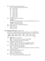
Figure 9.3
The yes/no nature of soldering success
Bridges and solderballs
A circuit board cannot function if it contains a short circuit, i.e. a solder bridge.
Wavesoldering without bridging demands special techniques, such as optimizing
the configuration of the wave (Section 4.4.4) and the board layout (Section 6.4.1).
Boards with a pitch below 1 mm40/mil are difficult to wavesolder without faults,
unless soldered in a nitrogen atmosphere.
With reflowsoldering, especially of fine-pitch boards, the type of paste and its
quality and the precision of the printing of it are key factors in achieving soldering
success (Section 5.2.3).
Solderballs need not necessarily be classed as soldering faults. If a solderball sits
between two neighbouring footprints on a fine-pitch board, it can constitute a
shortcircuit, and prevents the board from functioning. Elsewhere, solderballs repre-
sent potential shortcircuits, and as such reduce the reliability to an extent which is
difficult to quantify. How solderballs are to be regarded is very much a matter of
individual company policy.
Even a single soldering fault on a board prevents it from functioning, and there
are only two options: correct it or scrap the board. The choice between them
depends on several factors, which will be discussed in Section 10.1. What must be
stressed here is the following.
The nature of the soldering fault
The existence of a soldering fault is an objective fact. A joint is either soldered or it is
not soldered. A bridge is either there or else there is none. The soldering fault
presents a ‘yes/no situation’ (Figure 9.3). To pronounce upon it is in the nature of a
verdict upon an observed fact, and two or more inspectors must necessarily reach
the same verdict.
Because of its objective ‘yes/no’ nature, the success/fault verdict can be entrusted
to an automatic quality assessment system, which may be based on opto-electronic
inspection or functional electronic testing (Section 9.5.5).
Quality control and inspection 329
job:LAY09 page:6 colour:1 black–text
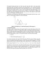
Figure 9.4
Some soldering imperfections
9.2.2 Soldering perfection and soldering imperfections
Assessing soldering perfection presents an inspector with a fundamentally different
situation: imperfect soldering does not prevent the affected circuit board from
functioning, but it can be seen as endangering or reducing its reliability. It may also
affect its saleability where the buyer has specified precise criteria.
Criteria for perfection may include the following features (Figure 9.4):
Wetting angle
Joint profile and amount of solder on a joint
Alignment or displacement of components
If an imperfection disqualifies the product in the eyes of the customer, it becomes
a soldering fault, because it makes the product unsaleable. A product which is
unsaleable does not work as far as the vendor is concerned.
Being saleable is the first function any manufactured product must fulfil. A
product which is not saleable in the market for which it has been made does not
function from the point of view of its maker (unless it is still saleable elsewhere for
less profit or at a loss). The offending feature must be corrected, or else the product
must be scrapped.
In contrast to the unequivocal yes/no verdict upon the verifiable fact of soldering
success or fault, a pronouncement upon the soldering perfection of a joint represents
a judgement, which is necessarily subjective. The judgements arrived at by different
inspectors represent points along a scale, which separate the ‘perfect’ or ‘acceptable’
from the ‘imperfect’ or ‘non-acceptable’ (Figure 9.5). On either side of the
accept/reject divide are areas of doubtful acceptability and false alarm.
It has been found that only 44% of the quality judgements on the same set of
soldered boards, made on two different days by the same inspector, agree with one
another. The quality judgements of the same boards made by two different inspec-
tors overlap by only 25%, while those made by three inspectors overlap by 14%
(A. T. & T. Bell, Burlington, N. Carolina).
To sum up: deciding between soldering success and a soldering fault amounts to a
verdict. Deciding whether soldering perfection has been approached sufficiently is a
matter of judgement, and the making of this decision can be automated only with
great difficulty.
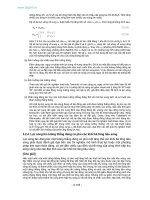
The blowhole problem
Blowholes in wavesoldered throughplated joints, caused by ‘gassing’ of the walls of
the hole, are a special form of imperfection (Figure 9.6).
330 Quality control and inspection
job:LAY09 page:7 colour:1 black–text
Figure 9.5
The perfect/imperfect judgement scale
Figure 9.6
Blowholes in a throughplated wavesoldered joint
The causes of gassing of throughplated holes, and the measures which are needed
in order to avoid it, are by now well understood. Gassing can be prevented by
ensuring the smoothness of the drilled holes and the continuity and adequate
thickness of the copper plating on their walls. It can be cured by a suitable heat
treatment of boards which are liable to form blowholes before using them.
Quality control and inspection 331
job:LAY09 page:8 colour:1 black–text
Because blowholes do not interfere with the functioning of a circuit board, they
are soldering imperfections rather than soldering faults, though their presence or
absence is an unequivocal yes/no situation. Searching investigations have shown
that they do not affect the life expectancy of joints or their reliability, in any way.
Corrective soldering can only mask, but not fill, a porous hole, and it is bound to
shorten the life expectancy of the joint.
9.3 Practical examples of soldering faults
The nature of a soldering fault means that a circuit board is faulty and cannot
function until every single fault on it has been corrected. Therefore, the most
important task of any quality-control system is to find every one of them. In Tables
9.1–9.3, the various types of soldering faults are listed and illustrated. For complete-
ness’ sake, faulty throughplated joints are included.
9.4 The ideal and the imperfect joint
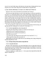
The criteria of perfection in a soldered joint go back to the days of handsoldering.
They have to do with two parameters: first, the wetting angle between the solder
and the substrate; and secondly the amount of solder in or on the joint. Together,
they determine the so-called joint profile. The ideal handsoldered joint has a ‘lean’
profile: the solder meniscus has a concave shape, so that the sharp wetting angle can
be seen clearly. Also, the contours of the ends of the joint members must be visible,
so that an inspector can be sure that, in the case of the leadwires of inserted
components, the wires do in fact project through the hole and that all leads have
been properly tinned (Figure 9.7).
The criteria of perfection of wavesoldered and reflowsoldered joints on circuit
boards go back to these early days. They deal with surface contours, surface areas,
the relationships between distances. It is possible to base judgements like good/bad,
acceptable/unacceptable or beautiful/ugly on these criteria, provided every inspec-
tor can refer to a set of pictures or samples of ‘perfect’ and ‘imperfect’ joints. It is
difficult and certainly expensive to derive a clear yes/no verdict unless precise,
time-consuming and therefore expensive measurements of individual joints are
made. It is equally difficult, if not impossible, to base an automatic, opto-electronic
inspection system on a ‘good/bad’ or ‘beautiful/ugly’ situation instead of a ‘yes/no’
one. Tables 9.4 and 9.5 illustrate practical examples of perfect and imperfect joints.
There is one instance where an imperfection can become a fault: ‘fat’ joints with
too much solder at the ends of a melf or chip-capacitor can cause the ceramic body
of the component to crack under the mechanical stresses caused by temperature
fluctuations during service. Fat joints hold the component as in a vice, lean joints
can yield.
9.5 Inspection
No circuit board should leave its soldering stage without having been inspected. To
inspect means to view or examine closelyandcritically.Thisimpliesthatinspection is
332 Quality control and inspection
job:LAY09 page:9 colour:1 black–text
Table 9.1 Soldering faults I: Open joints
Soldering Fault Possible cause
method (C, if correction is possible)
Wave No solder on both footprint
and wire or lead (C)
Solderwave did not reach the joint.
(If the joint was not fluxed, it is
covered by lumps of solder); or
the solderwave did not overcome
the shadow effect, because either
layout or waveshape was unsuitable.
Remedy: improve waveshape or
layout, or change orientation of the
board towards the direction of travel.
Reflow No paste on footprint. Check screen
or stencil for blockage
Wave Solder on wire or lead, but
not on land or footprint (C,
but difficult and costly)
Reflow Defect unlikely
With wired components: land
unsolderable through faulty
solermask or misplaced marking
With SMDs, as above or misplaced
adhesive
Reflow Wicking (C) Gap between leg and footprint, due
to lack of coplanarity of leads.
Remedy: quality control before
placement.
Unsuitable soldering parameters.
Remedy: put right, or choose paste
with higher-melting solder
more than ‘just having a look’. To be meaningful and cost effective, every inspection
procedure must have a set of well-defined targets or criteria, preferably in the form of
written, and sometimes illustrated, lists, or explicit software when automatic image
analysis is used.
The distinction between ‘soldering success’ and ‘soldering perfection’ (Section
9.2) simplifies the task of inspection, in the same way that it is easier to umpire a horse
race than a beauty contest. Without an umpire, both race and contest are pointless.
Without inspection, a manufacturing process like the soldering of electronic circuit
boards is incomplete.
There is a basic difference between the inspection of engineering products like a
crankshaft and the inspection of a soldered circuit board. The dimensions of the
Quality control and inspection 333
job:LAY09 page:10 colour:1 black–text
Table 9.2 Soldering faults II: Bridging and solderballs
Soldering Fault Possible cause
method
Wave Bridging between
neighbouring lands or
footprints (C)
Conveyor speed too high; unsuitable
wave geometry. Flux too thin or too
weak. Remedy: check (and change)
flux, or soldering parameters; if
layout unsuitable for wavesoldering,
change orientation of board in
carriage (does not always work)
Ditto, with fine-pitch
multileads
As above, or add solderthieves to
layout. Change direction of travel by
90°
Reflow As above (C) Paste tends to form solderballs.
Remedy: carry out solderballing test,
and if necessary use fresh paste.
Paste-printdown too thick: check
and if necessary, correct
Wave Solderballs near footprints (C) Can happen with controlled
atmosphere machines. Remedy:
change to different or slightly thicker
flux. Slow down conveyor
Reflow Paste forms solderballs or spits.
Remedy: if solderballing test
confirms, use fresh paste
Solderballs under melfs or
chips (C: de-solder and
resolder affected SMDs)
Printdown too large or too thick.
Remedy: check and correct screen
or stencil
Wave Scattered solderballs, or
‘spider’s webs’. (C: pick up
with tip of soldering iron)
Flux too thin, or insufficiently
pre-dried. Remedy: check and, if
necessary, adjust
Reflow Scattered solderballs. (C:as
above)
Paste spits because it has picked up
moisture, or temperature profile too
steep. Remedy: check and, if
necessary, use fresh paste or adjust
temperature profile of reflow oven
Note: As pointed out above,
solderballs do not necessarily
constitute a soldering fault, unless
they are loose, or are liable to
become loose, and can roll about on
the board
334 Quality control and inspection
job:LAY09 page:11 colour:1 black–text
Table 9.3 Soldering faults III: Displaced components
Soldering Fault Possible cause
method
Reflow One or more leads or faces fail
to connect with their
footprints (C: desolder and
resolder by hand)
Serious misplacement or floating.
Remedies: check pick-and-place
equipment; with chips or melfs, lack
of solderability at one end, or lack of
symmetry between footprints
Floating or tombstoning (C):
desolder and resolder
One end less solderable than the
other. One end solders later than the
other because of asymmetry of size
or thermal behaviour of footprints.
Remedy: check quality of
components or correct layout fault
Figure 9.7
The ideal handsoldered joint
former can be expressed numerically, and readily and automatically compared
against prescribed standards, within a given set of tolerances. It is very difficult, and
certainly expensive, to ascribe numerical values to a soldered joint. Hence the need
for visual, optical or functional inspection of soldered circuit boards.
9.5.1 When to inspect
Inspecting every soldered board when it has reached the end of the production line
is certainly necessary, but it is not enough. Unless intermediate inspections are
carried out after various stages of production, errors or defects which are carried
over into the next production stage can be very expensive to correct later.
The printdown of the adhesive which fixes SMDs to the board before wavesol-
dering must be checked for completeness and correct placement. Missing adhesive
means a lost SMD; misplaced adhesive can make adjacent footprints unsolderable.
Mistakes in adhesive printdown are very difficult and expensive to correct once
the joints have been cured. Most adhesives are given conspicuous, sometimes
luminescent, colouring to make visual or opto-electronic automatic inspection
easier.
Similarly, the correct printdown of solder paste must be checked before the
Quality control and inspection 335
job:LAY09 page:12 colour:1 black–text
Table 9.4 Too much or too little solder
Soldering Defect Judgement and possible
method remedy
Wave or None The ideal joint
Reflow H
1
H
!
+H
%
Wave Too much solder
H
1
9 H
!
+H
%
Acceptability depends on
the product category and
the customer. Remedy:
change machine
parameters, lower the
wave, speed up the
conveyor
Wave Too little solder
Reflow H
1
: 30%(H
!
+H
%
)
Acceptability as above.
Remedy: raise wave,
slow down conveyor,
more paste in case of
reflow
Wave Too little solder
Reflow W
1
: 75%W
!
Acceptability as above.
Remedy: check
solderability of footprint
and component
Reflow Too little solder on PLCC
J-leg W
1
: 50%W
!
Acceptability as above.
Remedy: see ‘wicking’
Table 9.5 Unsatisfactory wetting angle; displaced components
Wave Angle 990°
Reflow
Acceptability depends on
product category and
customer
D 9 50%W May be unacceptable
with fine-pitch layout.
In that case, count as
soldering fault
SMDs are placed on the board. Faults are easily corrected at this stage. If detected
after soldering in the form of empty joints or bridges, the cost of correction rises by
at least one order of magnitude.
With hand-placed components, a final check before the soldering stage is
advisable. Much mechanized pick-and-place equipment is equipped with integ-
rated checks for correct identity, polarity and placement of the components
(Section 7.4). If it is not, a final visual or optical check before soldering is worth
while.
336 Quality control and inspection
job:LAY09 page:13 colour:1 black–text
9.5.2 Visual inspection
It is useful to distinguish between two basic types of visual inspection, which one
could call the ‘general picture’ and the ‘detailed inspection’.
The general picture
In small-scale production, where boards are soldered individually, by hand or on
benchtop equipment, the operator will naturally look at every single board before it
leaves his workstation. If there is an obvious fault due to a malfunctioning of his
equipment, or a defective board, he or she will put matters right before carrying on
soldering.
With in-line soldering, the operator, or supervisor in charge of the soldering line,
whether wave or reflow, should have a brief look at the boards leaving the line at
regular intervals, perhaps at one board in every ten, in order to ensure that the line is
running normally. Obvious major faults might be unfluxed areas or uneven solder-
ing because of an unsteady solderwave, or reflowed boards which are scorched, or
did not get hot enough for the paste to melt on all joints. Unless such disasters are
spotted before many boards reach the next inspection station, the line may have
been producing a good deal of expensive scrap.
The detailed inspection
The manner of the detailed visual inspection and the equipment used for it depend
very much on the type and volume of production and the size of the boards. The
type and specification of optical inspection equipment ranges from simple or
illuminated magnifiers with a power of about five times, to sophisticated apparatus
with zoom optics, binocular operation, stereoscopic vision, and facilities to look at
the J-legs of PLCCs at an angle. The advent of low-priced, small, readily manipu-
lated video systems has added a new dimension to visual inspection.
As a general rule, optical systems where the operator has to look into a single
eyepiece, or a binocular, which forces him to keep his head in a fixed position, are
more fatiguing to operate than systems which show the object of observation on a
screen. A good and flexible system of illumination is essential with all optical
inspection methods. An easily operated handling system of the boards under test is
equally important. With a number of systems, boards are mounted on a movable xy
table, which allows for overall scanning, or indexing into preset positions where
certain recurring faults tend to occur.
Recent studies pinpoint the problems of visual inspection: operators, often
female, are under increasing stress, mental rather than physical, as boards get more
complex and the pitch gets finer. They rate their stress factors in descending order as
intense concentration, burden of responsibility and time pressure. Faulty ergonom-
ics and noise can be additional problems. With fine-pitch layouts and components,
the rate of inspection falls dramatically, and the stress is greater.
The solution is seen in systems where automated opto-electronic inspection
precedes, and is linked with, inspection by a closely integrated team of about three
operators, who visually inspect and manually correct faulty joints at the same time.
Quality control and inspection 337
job:LAY09 page:14 colour:1 black–text
The value of linking visual inspection with corrective soldering is increasingly
recognized and practised (Section 10.1).
9.5.3 Automated opto-electronic inspection
Unless the distinction between ‘soldering success’ and ‘soldering perfection’ is
made, automatic inspection must recognize both of them and be able to evaluate
features like joint contours. This demands expensive systems of great complexity. If
the judgement on soldering perfection is omitted, existing technology, which is
constantly being refined, permits relatively straightforward practical solutions for
automatically recognizing footprints without solder paste, empty joints or the
presence of bridges or solderballs. These systems are based on video scanning of a
board surface, combined with an automatic comparison between the actual image
and the ideal image of a faultless board. Equipment which operates fast enough to
keep up with in-line soldering machines and reflow installations is commercially
available.
Opto-electronic systems are able to recognize the following soldering failures:
Missing, misplaced or defective printdown of solder paste
Missing or misplaced adhesive
Missing, misplaced or displaced components
Bridges, ‘spider’s webs’ and solderballs
A recently developed automatic opto-electronic inspection system does not re-
quire a pre-programmed ‘ideal’ image of a faultless board, but creates its own
‘learning curve’ by evaluating parameters such as shape of solder-fillet, identity and
dislocation of components, bridges etc. ‘Self-learning’ automated visual inspec-
tion equipment is expected to become commercially available before the end of
1997.
9.5.4 X-ray inspection
X-ray inspection represents an optical system, which operates at two levels. The
board with its joints is scanned by penetrating X-ray radiation, which is absorbed
most strongly by the lead-containing solder in either joints or paste printdown, less
so by metallic conductors, ICs and other semiconductor devices, and least of all by
organic substances like FR4 and ceramic or plastic component housings. The
resulting X-ray image is converted to a monochrome image in the visible range,
which can be evaluated visually by an operator, or processed photo-electronically as
described above, and compared with the image of a faultless board. One of the
problems which might perhaps be encountered in this context with lead-free solders
(Section 3.2.3) is the reduced contrast between such a solder and its surroundings in
an X-ray image, unless the solder contains bismuth.
X-ray images are shadowgraphs. In the last decade, X-ray sources have been
developed with emitter-spots small enough to provide shadows of sufficient sharp-
ness to allow even micrographic evaluation. By controlling the voltage applied to
338 Quality control and inspection
job:LAY09 page:15 colour:1 black–text
Figure 9.8
X-ray images of capillary joints. (a) Innocuous cavities caused by
trapped air or vapour; (b) pattern of unsoundness indicating a wetting or
solderability problem.
Solder,
void
the X-ray tube, the penetrating characteristics of the radiation can be adjusted to suit
the features which need to be examined.
X-rays show up the solder in the joint itself, which is a great advantage, but the
image must be sensibly interpreted: as has been explained in Section 3.6.3 (Figure
3.19), almost all capillary joints contain voids. A distinction must be made here
between two kinds of joint porosity. If the porosity appears as voids which are
surrounded by solder, it is safe to conclude that the solder has wetted the joint
surfaces with a satisfactory, sharp wetting angle. This type of porous joint will be as
reliable as a completely filled one. If, however, the solder in the joint gap appears as
an archipelago of separate islands, one of the joint surfaces is likely to have dewetted
(Figure 9.8), and reliability of the joint is impaired. Image processing software might
well be devised to be able to distinguish between these two types of
porosity, where the solder forms either a continuous or a discontinuous phase, and
raise the alarm with dewetted capillary joints.
X-ray inspection is the only option for inspecting joints underneath BGAs and
flip-chips (see Section 2.2). To spot an open joint between a solderbump and the
paste print-down on the board is difficult, because the bump itself will produce a
circular shadow. A strategy to overcome this problem has been proposed by N.
Manson. The pads on the board and the paste print-down are both given
diamond-shaped or square outlines. A square shadow means that the paste has been
melted, but has not been drawn into the joint. A round X-ray shadow indicates a
correctly formed joint. It should not be difficult to program an automatic opto-
electronic X-ray inspection system to recognize this type of defect. The discovery of
an open joint underneath a flip-chip poses a problem: once the underfill underneath
the chip has set, the chip cannot be removed without damaging the board, and the
cost of scrapping the board must be balanced against the costly and delicate
microsurgery needed to clear away the underfill.
There is no reason why the adhesive for fixing SMDs prior to wavesoldering
should not be made opaque to X-rays by the addition of a filler like a barium
compound. Thus, X-ray scanning could be used for the intermediate scanning of
boards for the correct presence of either adhesive or solder paste before placing the
components. X-rays are equally suitable for checking the correct placement of
components before the boards enter their soldering stage. The virtues of such
intermediate inspections between successive manufacturing stages are obvious.
Quality control and inspection 339
job:LAY09 page:16 colour:1 black–text
9.5.5 Electronic inspection
Testing the correct functioning of a circuit board by electronic means has developed
into a complex technology which is outside the scope of this book. ATE testing
with an array of probes, not so long ago a cause of concern for solder paste
formulators, is still being practised but on a declining scale. The growing number of
functions, crowded not only on to a board, but also into individual components and
MCMs, demand that the board itself is designed for testability – for example by
methods such as ‘boundary scanning’. Dedicated contact points are designed into
the board circuitry, from which the board can be interrogated for its functions, as
well as for the existence and location of soldering faults. Functional testing of
soldered boards has become an important capital- and cost-intensive part of elec-
tronic production. It is still in a state of constant further development.
9.5.6 Thermographic inspection
For the sake of completeness, the so-called thermographic methods of sequentially
checking all the joints on a board for their quality by measuring their thermal
capacity must be mentioned here. The basic idea is to find out whether there is too
much or too little solder on any given joint, or whether the joint is open, by
measuring its thermal capacity and comparing it with an ideal value.
In order to do this, a short, accurately dosed pulse of Nd: YAG laser energy is
focused onto the joint, and its temperature rise is picked up by a fast-response
pyrometer and recorded. Naturally, the reflective properties of the solder fillet on
which the laser beam is focused also enter into the result and the evaluation of the
test. The method requires a laser scan of great accuracy and, for a start, a board with
every joint of an adequate degree of perfection – a so-called golden board – so that
for every type of board, a library of ideal thermal capacities can be established.
The Vanzetti method was and still is used, especially with military and space
electronics. Other, similar, thermographic testing systems have been developed in
Europe, but are not commercially available at the time of writing (1997).
9.6 References
1. Birolini, A. (1992) Guidelines for the development and design for quality,
reliability and maintainability. Report Z4, 10 January 1992, Swiss Fed. Inst.
Technology, Zurich.
2. Lea, C. et al. (1987) The Scientific Framework leading to the recommendations
for the elimination of Blowholing in PTH Solder Fillets. Circuit World, 13, No.
3, pp. 11–20.
3. Lea, C. (1990) The harmfulness of reworking cosmetically defective joints.
Soldering and SMT, No. 5, pp. 4–9.
4. Strauss, R. (1992) The Difference between ‘Soldering Success’ and ‘Soldering
Quality’; Its Significance for Quality Control and Corrective Soldering. Proc.
6th Intern. Conf. Interconnection Technol. in Electronics, Fellbach, DVS Report 141,
Duesseldorf, Germany (in German).
340 Quality control and inspection
job:LAY09 page:17 colour:1 black–text
5. Vanzetti, R. (1984) Automatic Laser Inspection System for Solder-Joint Integ-
rity Evaluation. Proc. 3rd PC World Convention, Washington DC, Paper WC
III-44.
6. Geiler, H. D., Karge, H. and Kowalski, P. (1992) Possibilities and Limits of
Modulated Thermographic Spectroscopy for the Nondestructive Testing of
Joints. 6th International Conference on Interconnection Technology in Electronics,
Fellbach. D.V.S. Report 141, Duesseldorf, Germany, pp. 111–112.
7. Graumueller, B. et al. (1997) Non-destructive Examination of Soldered Joints,
VTE (3) June, pp. 145–149 (in German).
8. Manson, N. (1996) Qualification Requires Keen Vision. Electronic Production,
July/August, pp. 15–16.
Quality control and inspection 341
job:LAY10 page:2 colour:1 black–text
10 Rework
10.1 The unavoidability of rework
10.1.1 Rework in the production process
In our imperfect world, zero-fault soldering does not exist. Soldering faults will
occur, and because even one single fault makes a board unusable, each must be
corrected by rework or corrective soldering.
It would be a mistake to regard rework as an unavoidable, tedious adjunct to
electronic production. On the contrary, it is an essential link in the production
chain. Unless it is taken seriously, properly organized, managed, monitored and
integrated into production, reworking the soldered boards may well cost more than
soldering them in the first place.
On the other hand, if rework is monitored systematically, so as to lead to a
learning curve and a fault catalogue for each type of board, its cost can be reduced to
its unavoidable minimum. At the same time, the fault catalogue will form a valuable
tool, for use by management, designers, buying departments and quality managers.
This applies equally to a large organization or manufacturing unit with many
soldering lines as to a small manufacturer with a handful of employees.
Every rework operation must involve three steps:
1. Diagnosis Having located a fault which must be put right, try to find out first
why it has occurred. Don’t start working on it, until you have satisfied yourself
that you have found the answer, and have made a record of it. Otherwise, you
may destroy vital evidence, which could have helped to prevent the fault
recurring again.
2. Remedy Put the fault right.
3. Prevention Make sure that whoever in the organization could or should have
prevented the fault from occurring, knows what you have found and done
about it, and if possible that this information is recorded. Procedures and
information technologies to take care of that are commercially available (Sec-
tion 10.5.2). The rework rate can be regarded as the fever thermometer of a
manufacturing line. If nobody cares to read it, the patient may well be
moribund before anybody has noticed that he is sick.
job:LAY10 page:3 colour:1 black–text
10.1.2 Desoldering and resoldering
Rework itself often involves two closely linked operations: if the correction of a
fault requires the removal of a faulty, misplaced or dislodged component and its
replacement, the desoldering and resoldering operations which this implies should
follow closely upon one another.
Removing bridges and, if necessary, solderballs, are simple desoldering oper-
ations. Desoldering leaded components from throughplated holes requires soldering
irons which can suck the solder out of the hole. With SMDs, the removal of a
defective component and its replacement with a new one can often be carried out
with one and the same tool. With the desoldering of wavesoldered SMDs, separat-
ing the glued joint underneath the component is an additional operation. Open
joints are normally filled with a small temperature-controlled handsoldering iron.
10.2 Basic considerations
10.2.1 Metallurgical and mechanical consequences of rework
A reworked joint is never as good as the first joint would have been had it not
needed to be replaced or corrected. The reasons are found principally in the
metallurgy of joint formation. Furthermore, the additional thermal, and sometimes
mechanical, stresses of resoldering may easily weaken the bond between footprint
and board. A lifted footprint is one of the most serious types of damage, caused by
getting a joint too hot or heating it for too long during desoldering. Repairing a
lifted footprint is possible, but it is expensive, takes time, and the board will never be
as good again as it was in the first place.
Industrial experience confirms the damaging effect of corrective soldering. So
did a cooperative research project carried out by a number of industrial companies
in the UK under the auspices of the National Physical Laboratory.
The latter counted the number of through-hole joints on standardized sample
boards with 2000 joints each which showed visible cracks after they had been
reworked with a soldering iron under controlled conditions and then exposed to up
to 1000 temperature cycles between −20 °C/−4 °F and 100 °C/212 °F. For com-
parison, boards which had not been reworked were given the same thermal
treatment. Some of the results are given in Table 10.1.
Two conclusions are clear:
1. The longer the rework contact time of the soldering-iron bit, the more
soldered joints are visibly cracked after a given number of thermal fatigue
cycles.
2. The higher the rework temperature, the more heat is supplied to the solder
joint and the greater is the degradation of its performance under thermal
fatigue, i.e. the loss of reliability.
The metallurgical reason for this degradation is the growth of the brittle intermetal-
lic layer between solder and substrate. Its thickness is a function of the confrontation
time between the molten solder and the substrate, and of its temperature.
Rework 343
job:LAY10 page:4 colour:1 black–text
Table 10.1 The degradation of soldered jonts caused by rework
Rework time at soldering
temperature of 400 °C/750 °F
Number of joints out of 2000 cracked after 2000 cycles
between −20 °C/−4 °F and 100 °C/212 °F
No rework 100
2 sec 160
6 sec 180
Rework temperature using
rework time 4 sec
Number of cracked joints after cycles as above
350 °C/660 °F 130
400 °C/750 °F 170
450 °C/840 °F 200
A further factor is the depletion of tin in the immediate neighbourhood of the
solder/copper interface because it migrates to augment the intermetallic layer. This
leaves a predominance of lead in the area next to that layer. Lead being weaker than
solder, this circumstance further promotes cracking under thermal fatigue loads.
10.2.2 The cost of rework
Rework is a joint-by-joint procedure, and necessarily time-consuming and expen-
sive. Reworking a single joint costs on average as much as did the first-time
soldering of the complete circuit board on which it sits, and often considerably
more. Depending on the type of product and its sale value, it may sometimes be
cheaper to scrap a faulty circuit than to rework it. Some low-cost products like
pocket calculators, cheap electronic watches and toys fall in that class.
In small-scale production in particular, where visual inspection and rework are
carried out by the same operator or operators, it is important to keep this cost aspect
in mind. It is tempting to say ‘I might as well touch up this joint while I am looking
at it.’ Not only do joint quality and reliability suffer through this practice, but costs
are liable to rise in an uncontrollable manner.
10.2.3 Lessons to be learned
The lessons to be drawn from these considerations are plain:
1. Whatever the method used for rework, choose only the best equipment
available, and maintain it in top condition.
2. Complete every joint quickly. The solder should be molten for not longer than
a few seconds.
3. Keep the working temperature as low as is compatible with this requirement.
4. Preheating the board, either locally or overall, before carrying out any rework
on it brings two benefits. First, the specific heat of the FR4 substrate is almost
344 Rework
job:LAY10 page:5 colour:1 black–text
four times that of copper or solder. This means that four times as much heat
energy is needed to bring the board up to soldering temperature than to heat
the joint itself. Preheating considerably shortens the heating time necessary to
complete a joint, particularly with heavy multilayer boards.
Secondly, with wavesoldered boards where the SMDs are glued to the board
surface, preheating softens the adhesive joint and makes it easier to break when
desoldering becomes necessary (Section 4.9.5). A preheating temperature of
about 60 °C/140 °F to 100 °C/210 °F is usually enough for this purpose.
A stream of warm air directed against the underside of the board is the usual
method of preheating. This avoids the danger of a sharply localized hot spot,
which could distort the board.
5. Rework for cosmetic reasons alone is an expensive and damaging luxury, and it
should only be carried out if the customer or the market demands it and pays for
it.
10.3 Rework equipment
10.3.1 Heat sources
Almost every heat source which is employed in production soldering finds its use in
rework: soldering irons in various forms, thermodes, solderwaves in miniature
form, infrared radiation, hot air or gas, and in recent years also the vapour of a
vapourphase soldering machine. With all of them, efficiency of the heat transfer
from source to joint is of the essence, together with precise temperature control.
Soldering irons
Molten solder is the ideal heat transfer medium: its heat conductivity is high and,
being molten, it adapts perfectly to the surface contours of the joint and the joint
members. For this reason, a soldering iron used for rework must have a well tinned
tip, preferably with a drop of molten solder on it, to establish instant and good
thermal contact with the joint. The best solder to use for rework, not only with an
iron but with any method, is the silver-containing 63% tin solder (Section 3.3.1).
The size of the iron and the shape of the tip must suit the type and the
configuration of the joint, as will be shown in Section 10.3.2. Naturally, the
ergonomic aspects of the hand-held soldering iron must not be neglected.
Precise control of the tip temperature, and a fast response to changes in the
amount of heat demanded from it, are very important. Recent years have seen rapid
advances in the technology of the soldering iron, which had remained static through
several decades. Above all, methods of heating the soldering tip, and of shortening
the path from the heat source to the end of the tip, have improved it
greatly. Many handsoldering work stations include a fast response temperature
indicator of the soldering tip itself.
Bearing in mind what is at risk if rework is carried out badly, it is worth stressing
the importance, not only of choosing a state-of-the-art soldering tool with antistatic
Rework 345
job:LAY10 page:6 colour:1 black–text
protection and a quick response to sudden heat-demands or changes in thermostat
setting, but also of maintaining it well and periodically checking the accuracy of its
temperature control.
Heated tweezers and thermodes
Resistance-heated tweezers are a convenient tool for desoldering the two end-
joints of a melf or chip simultaneously. PLCCs can be removed with a shaped
tweezer, which grips the vertical shanks of the J-legs on all four sides of the
components simultaneously. Tweezers are particularly useful for removing and
resoldering these components on a crowded board, where the neighbours of the
affected component must be protected from the soldering heat of the site of the
repair (see below). Tweezers, like thermodes, are made from an untinnable metal
like tungsten.
The thermodes used for desoldering are the same as those which are used for the
impulse-soldering individual multilead SMDs (Section 5.7). Because their soldering
surfaces are untinnable, they cannot be pretinned like a soldering iron, and molten
solder cannot be used as a thermal link between the tool and the joints. A thin
coating of a low-solids RMA flux, brushed over the row of leads on all four sides,
will have to serve as a substitute for the molten solder in establishing a thermal link
between the soldering tool and the joint. Once the thermode sits firmly on the flat
leads, the heat transfer between the soldering tool and the joints takes place by
conduction, as with a tinned soldering iron.
Miniature solderwaves
Miniature solderwaves were developed in the sixties for the desoldering and
resoldering of inserted multipin devices, like DILs. With this method, the board is
placed over the nozzle of a dedicated small wavemachine, so that the leads which
have to be desoldered sit closely above it. As soon as the wave is switched on and
touches the underside of the board, the solder in the joints melts and the DIL can be
lifted off. A replacement DIL can then immediately be soldered into the empty
holes, its legs having been fluxed first. Alternatively, the molten solder can be
sucked out of the holes, an operation for which this type of machine is equipped,
and the replacement part can be soldered in position, on the same wave, at a later
stage.
Hot air or gas
Jets of hot air or gas, of a controlled temperature, are widely used for desoldering
SMDs. Because they transfer their heat to the joints by convection, which is much
less efficient than conduction through molten solder or contact with a thermode
(Section 5.5), it takes longer to melt the solder in the joints, and this must be taken
into account when deciding on the reworking procedure.
Single jets from hand-held nozzles can be used for desoldering and resoldering
346 Rework
job:LAY10 page:7 colour:1 black–text
melfs, chips, SOs and multilead devices. For the latter, however, many vendors offer
equipment with interchangeable arrays of jet nozzles, which direct the hot air or gas
towards the joints on all four sides of the SMD at the same time. These jet arrays are
useful for the desoldering and resoldering of PLCCs, where the joints are not
directly accessible to a plain thermode.
The hot air stream from a hand-held nozzle is usually controlled by the operator
via a pedal, while multijet soldering heads are operated by a timer, the correct
duration of heating having been determined empirically for a given board and
component. With most hot-air desoldering machines, the board is preheated locally
from underneath, for reasons already mentioned. Preheating is especially important
with heavy multilayer boards.
Infrared radiation
Beams of infrared radiation, focused on the joints of a multilead device, are another
option for supplying the heat for desoldering and resoldering. Similar to the jet
nozzles, the IR desoldering heads are interchangeable to suit specific component
dimensions. Heating by radiation represents a non-equilibrium system (Section 5.8)
where the temperature of the heat source is much higher than the target tempera-
ture of the joint. For this reason, such systems demand precise dosage of the
radiation input, and ideally a feedback from the joint temperature to the heatsource.
Infrared desoldering heads normally operate with medium wavelength emitters,
operating in the 300 °C/550 °F to 500 °C/950 °F range.
10.3.2 Rework stations
The workplace or work station for carrying out desoldering and resoldering must be
user-friendly. Reworking can be a stressful task, and requires constant concentra-
tion and decision making. The workplace must therefore be well lit, provided with
an exhaust which removes the flux fumes, and the equipment must be ergonomi-
cally designed so that it can be operated with a minimum of fatigue.
For manual rework, adjustable inclined frames which hold the board are standard.
Wide-field magnifiers with a power which need not exceed five, or at most ten,
times are also standard. Often, provision is made for a set of soldering irons of
different size to be readily at hand. In addition to soldering irons, workstations may
provide sets of hot air or gas jets, vacuum pipettes for handling components, and
heated tweezers for desoldering and resoldering them. Small mechanical tools like
rotary drills and reamers to clean or remove footprints are also often part of a rework
station.
More elaborate manual stations are fitted with an overhead illuminator, which
direct a pencil of light in sequence to the several joints or components which
require rework. This sequence can be created by the inspection station and stored
on software in cases where visual inspection and manual rework are carried out
separately from one another.
From simple manual workstations, the market offers a gradual succession of
Rework 347
job:LAY10 page:8 colour:1 black–text
increasingly complex and sophisticated equipment for rework, particularly for use
with multilead SDMs. Most of them use sets of quickly interchangeable hot-air
nozzles or thermodes, together with placement systems for aligning the component
to be dealt with accurately with the soldering tool, visually or by opto-electronic
means.
Notwithstanding these electromechanical aids, the accuracy of feedback between
the human eye and hand must not be underestimated. It has been shown that a
trained operator, aided by a low-power magnifier, can place a multilead device with
a 0.5 mm/20 mil pitch on its footprints with sufficient accuracy by hand. This means
a lateral accuracy of ±0.125 mm/5 mil, since the maximum permissible lateral
misplacement of fine-pitch components is one quarter of the pitch distance (M.
Cannon, Pace Europe Ltd, verbal communication).
10.4 Rework tasks and procedures
Most of the published information and know-how in this field can be found in the
voluminous vendors’ literature. A few comprehensive accounts have appeared in
the technical press.
–
10.4.1 Removing bridges and solderballs
A solder bridge is removed by touching it briefly, for not more than a few seconds,
with the well-tinned tip of a small soldering iron, with a rated output of about 40 W,
and set to a temperature of about 250 °C/480 °F. For de-bridging fine-pitch leads, a
conical 20 W soldering bit is best. All that is necessary is to disrupt the bridge. Do
not try to ‘tidy up’ the joints on either side, and do not use flux. A solder wick (see
below) should not be used either, because it is likely to suck out too much solder
from the joints themselves and thus weaken them.
Solderballs are removed in the same way. As soon as the tip of the iron touches
one, it will disappear. The same will happen with ‘spiders’ webs’. Because a web
covers more ground than a solderball, a chisel-shaped soldering tip is more conveni-
ent for removing them.
Excess solder is removed from the tip of a soldering iron by wiping it with a piece
of linen or cotton, but never with fabric made from synthetic or mixed fibre. Many
handsoldering stations are equipped with a heat resistant sponge for cleaning the
soldering tip.
10.4.2 Desoldering SMDs
Any of the following circumstances makes desoldering of an SMD obligatory:
E Melfs and chips, if one or both of their metallized faces are seen to be badly
solderable or unsolderable, or if the metallization has been leached off by the
molten solder. The desoldered components are discarded.
E Chips which have ‘tombstoned’. The desoldered components are discarded,
because their solderability is doubtful.
348 Rework
job:LAY10 page:9 colour:1 black–text
Figure 10.1
Desoldering a melf or chip with a solder-wick
E Melfs, chips and SOs which have floated away from their footprints. The
desoldered components are discarded, unless there is a desperate need for their
re-use.
E Any SMD which is in the wrong place, or wrongly orientated. If carefully
desoldered, the component can be reused.
If X-ray inspection or functional testing reveal an open joint underneath a BGA, the
offending component must be desoldered, because the joints underneath are inac-
cessible, and cannot be corrected with the component in position. The BGA itself
should be discarded, unless it is irreplaceable. To put fresh solderbumps on the
underside of a desoldered BGA is a delicate and laborious operation, though solder
pre-forms for putting down a fresh array of bumps are on the market. Unless the tem-
perature is carefully controlled, the operation could easily ruin the IC inside the com-
ponent, or cause the housing to crack due to the ‘popcorn’ effect (see Section 2.6).
Flip-chips pose another problem: once the underfill has been applied and
hardened, it is almost impossible to remove a flip-chip without damaging the board.
Delicate microsurgery with special tools would be required to cut away the
hardened underfill without damaging the board. The cost of this operation, which
may put the board at risk in any case, must be balanced against the cost of scrapping
the board (see Section 9.5.4).
Desoldering melfs and chips with a solder-wick
Melfs and chips are joined to their footprints by butt joints. The joints of the larger
ones contain too much solder to be sucked up by the tip of the hot soldering iron.
Instead, a device called a ‘solder-wick’ is used to remove it. A solder-wick is a tape
of closely braided fine copper wire, a few millimetres wide, which is impregnated
with an RMA flux. Recently, solder-wick impregnated with a no-clean flux has
become available. The wick acts towards molten solder like blotting paper against
ink: for desoldering, it is pressed into the corner between the endface of the
component and the footprint (Figure 10.1) with the end of a chisel-shaped soldering
Rework 349
job:LAY10 page:10 colour:1 black–text
Figure 10.2
Twisting a glued joint apart
tip held at a temperature of about 250 °C/480 °F–300 °C/570 °F. As soon as the heat
has travelled from the tip through the wick of the solder, the latter melts and is
sucked by capillarity into the fluxed wire braid. Tip and wick are lifted off, and the
solder-filled end of the wick is discarded. This operation should take no longer than
a few seconds, but the wick should be pressed into the corner for long enough to let
the heat travel into the gap underneath the component so that all the solder is sucked
out of it.
With wavesoldered components, the glued joint between component and board
must now be broken. To make this possible without undue force, the adhesive must
be heated to above its ‘glass-transition temperature’, which is normally about
60 °C/140 °Fto80°C/180 °F. Above that temperature, the adhesive changes from a
rigid body to a soft pliable substance (Section 8.5). This makes it possible to break
the glued joint by twisting the component (Figure 10.2).
If the temperature is not high enough and the adhesive still too stiff, the board
might get damaged. If there are any conductor tracks running underneath the
component, between its footprints, the glued joint sits on top of the soldermask
which covers them: twisting the joint apart with too much force can damage the
soldermask and expose the tracks underneath. Local preheating of the board will
raise the temperature enough to soften the adhesive. The heat of the desoldering
will do the rest. If this is not enough, further heat from a hand-held hot-air nozzle
will have to be applied to the component.
Desoldering melfs, chips and PLCCs with heated tweezers
A simpler method of removal employs a pair of tweezers, heated in the same manner
as a thermode to about 220 °C/400 °F. In this way, the joints at both ends of a
component are desoldered simultaneously. The jaws of the tweezers are pressed
against the ends of the component until the solder can be seen to melt. As soon as
this happens, the component is lifted off or, in the case of a wavesoldered one,
twisted from its adhesive joint (Figure 10.3).
350 Rework
job:LAY10 page:11 colour:1 black–text
Figure 10.3
Desoldering with heated tweezers
The same principle, using tweezers with interchangeable heated jaws which
enclose the sides of a PLCC, is a useful option. The jaws press against the sides of the
J-legs, and the component is lifted or twisted off as soon as the solder melts.
Desoldering SOs, SOICs and multilead components
With these components, the leads cannot be gripped with a sideways pressure
without damaging them, which would be undesirable where removed components
may have to be re-used. Here, a heated tool of a shape which conforms to the
pattern of the footprints, in other words a thermode as it is used in impulse soldering
(Section 5.7), is pressed downwards against the horizontal ends of the gullwing legs
(see Section 5.8.3).
The hot jaws only heat the joints, but do not grip the leads. Lift-off is effected by a
vacuum pipette, which is located between the jaws and seats against the top of the
component housing. It is activated by the operator when the joints are seen to have
melted and the component is ready to be lifted.
With thermode desoldering, a thin coating of RMA flux brushed over the
component leads improves the thermal contact between them and the face of the
thermode. The presence of flux also reduces to some extent the sharp spikes of
solder which are likely to remain on the footprints after the component has been
lifted clear.
Failing desoldering equipment which allows the use of a thermode, multilead
components can be desoldered joint by joint, with a temperature-controlled solder-
ing iron (about 220 °C/430 °F). The well-tinned tip of the chisel-shaped iron is
pressed against the joint: as soon as the solder is seen to melt, the iron is lifted off and
the gullwing leg is lifted clear of the footprint with a pair of tweezers. Another way
is to thread a thin stainless steel wire underneath the component: as soon as the joint
has started to melt, the legs are pulled upwards with the wire, one after the other
(Figure 10.4). After desoldering operations such as these, the component is mostly a
write-off because of its bent legs. Also, unless skilfully executed, these methods put
the footprints in danger of lifting off the board because of overheating. For all these
reasons, it is best to invest in a thermode desoldering tool.
Rework 351
job:LAY10 page:12 colour:1 black–text
Figure 10.4
Desoldering a SOIC leg by leg (courtesy Edsyn Corp.)
Desoldering BGAs
Several vendors offer special equipment for desoldering a BGA if it must be
removed because one of its joints is defective, because it is wrongly orientated or
because it malfunctions. These desoldering tools or stations are of varying degrees of
sophistication, working with hot air or hot nitrogen (230–250 °C/420–480 °F),
which is directed against the upper surface of the component, less frequently with
infrared heat. When desoldering, the underside of the board is heated to about
100 °C/210 °F to assist the melting of the soldered joints. As soon as the correct
desoldering temperature has been reached and the joints have melted, the device is
lifted off with a vacuum pipette. After the lift-off, the vacated footprints are
cleaned up as described below. A small amount of no-clean flux, applied to the edge
of the BGA and allowed to penetrate into the gap underneath by capillarity, will
reduce the amount of ‘spiking’ of the solder which is left on the footprints after the
BGA is lifted clear.
These soldering stations are designed not only to remove an offending BGA, but
also to solder its replacement on to the board. With some of them, the solder-bumps
underneath the replacement BGA can be accurately aligned with their footprints by
optical means. With others, fiduciary markings on the board have to be relied upon.
It has been suggested that reworking BGAs will be facilitated if a 5 mm/0.2 in
wide ‘keep-out’ zone around the BGA site can be kept free of neighbouring
footprints – provided the board designer can be persuaded of its merits.
352 Rework
job:LAY10 page:13 colour:1 black–text
Desoldering in a vapourphase machine
Equipment has been described recently which allows the desoldering of multilead
devices and BGAs in a standard vapourphase installation. The top surface of the
component to be removed is fastened to the arm of a small lift-off device, which is
placed next to it on the board. The board is then put in the vapourphase chamber.
As soon as it has reached a pre-set temperature, say 190 °C/375 °F, the lift-off
mechanism is actuated and pulls the component away from the board. Advantages
claimed are the absence of spikes on the footprints, and of any surface oxydation. A
possible drawback could be the fact that with this procedure all the joints on the
board, not only those to be desoldered, are heated to above the melting point of the
solder.
Cleaning the empty footprints
Before the replacement component is put into place, the footprints must be cleared
of remaining blobs or spikes of solder. This is done by lightly fluxing them again and
then passing the tip of a soldering iron, preferably chisel-shaped, across all of them.
After that, they are fluxed once more, and the replacement SMD is soldered into
place as soon as possible.
Caution!
Any footprint cleared of solder must be given a coating of flux as soon as possible, for
the following reason: if the soldercoating is removed from a footprint, or for that
matter from any soldered copper surface, the top layer of the diffusion zone formed
by the intermetallic compound ‘eta’ (,Cu
Sn
) (Section 3.1) should be exposed to
the air. This compound will immediately begin to oxidize and become unsolder-
able, even with a strong flux, unless it is quickly protected from the atmosphere by a
thin coating of flux. All the same, a replacement component could be soldered to its
footprints as soon as possible. Should this compound by any chance have begun to
oxidize and made the footprint unsolderable, the situation can be retrieved by
rubbing it with a piece of fine emerypaper, folded over the end of a small
screwdriver, until the pink copper surface becomes visible.
10.4.3 Filling empty joints
Finding the empty joint
An empty butt joint or open joint is easily recognized provided it is fully visible.
PLCCs are the exception, because they are half hidden under the component edge.
With a little practice and the right optical aid this problem is easily overcome. With
BGAs, the joints are underneath the component and faults can only be identified by
X-ray inspection (see Section 9.5.4).
With empty capillary joints, only the top surface of the component lead is directly
visible. A bent lead or a footprint without solder is immediately apparent. If the
footprint is covered with solder, but the solder along the edge of the lead looks
doubtful or if there is none at all, the joint can be tested by lifting the end of the lead
Rework 353