ENCYCLOPEDIA OF MATERIALS CHARACTERIZATIONC phần 10 pdf
Bạn đang xem bản rút gọn của tài liệu. Xem và tải ngay bản đầy đủ của tài liệu tại đây (1.72 MB, 71 trang )
to what sensitivities for
NRA
will be without considering the specific reactions and
sample materials involved in each case. However, sensitivities on the order of
10-
100
ppm are common.
Other Considerations
Sample Requirements
The maximum sample size is limited only by the design
of
the sample chamber.
Typically, samples up to several cm in diameter can be accommodated.
A
diameter
of a
few
mrn
is
generally the lower limit because high-energy ion beams focused
through standard beam optics are on the order of a
fay
mm in diameter: however,
microbeam setups permit the use of samples an order of magnitude smaller.
Nonconducting samples require special consideration. The incident ion beam
causes a buildup of positive charge on the sample surfice. Discharging of the sam-
ple may create noise in the spectrum collecced by surfice barrier detectors. In addi-
tion, the presence of accumulated positive charge on the sample may affect the
accuracy of current integration systems, making it difficult to determine the exact
beam dose delivered to the target. This problem may be obviated by flooding the
sample surface with electrons to compensate for the buildup of positive charge
or
by
depositing a thin layer of conducting material on the sample surface. If the latter
option is chosen, the slowing down of ions in this layer must be cansidered when
calculating depth scales. In addition, care must be taken to select a material that will
not experience nuclear reactions that could interfere with those of the species of
interest.
Accidental Channeling
Effects
When analyzing single-crystal samples, the experimenter should be aware that acci-
dental channeling may occur. This happens when the sample is oriented such that
the ion beam is directed between rows
or
planes of atoms in the crystal, and gener-
ally results in reduced yields from reactions and scattering from lattice atoms. Such
effects may be minimized by rotating the target in such a way to make the direction
of the beam on the target more random. In some cases, the use of molecular ions
(i.e.
H2+
or
H,+
instead of
H+)
can also reduce the probability of accidental chan-
neling. The molecular ions break up near the sample surface, producing atomic
ions that repel and enter the material with
more
random trajectories, reducing the
likelihood of channeling.
However, when deliberately employed, channeling is a powerful tool that may
be used to determine
the
lattice positions
of
specific types of atoms
or
the number
of
specific atoms in interstitial positions (out
of
the lattice structure). Further infor-
mation on this technique is available.’
11.4
NRA
689
Simulation Programs for
NRA
There are a number of computer codes available6. to simulate and assist in the
evaluation of
NRA
spectra. Most of these programs are similar to
or
compatible
with the
RBS
simulation program RUMP. These programs require the input of
reaction cross sections
as
a hction of incident ion energy for the appropriate
beam-detector geometry. The user interactively fits the simulation to the data by
adjusting material parameters, such
as
the bulk composition and the depth distri-
bution of the component being profiled. SPACES6 is designed to deal specifically
with narrow resonances (e+,
27Al
(p,
y)
28Si at
992
kev) and their associated dig-
culties, while SENRAS7 is useful in many other cases.
Applications
In this section, a number of applications for
NRA
are presented.
As
this is not a
review article, the following is only a sampling of the possible
uses
of this powerful
technique. The reader interested in information on additional applications is
directed to the proceedings of the Ion Beam Analysis Conferences' and those from
the International Conferences on the Application of Accelerators in Research
and
Industry, among other sources.
9
Hydration Studies of Glass
A combination of nudear reactions have been used in studies of the processes
involved in the hydration and dissolution of glass. Lanford et
al."
investigated the
hydration
of
soda-lime
glass
by measuring Na and
H
profiles. The profiles
(Figure
5)
indicate a depletion of sodium in the near-surface region of the
glass
and
a complementary increase in hydrogen content. The ratio
of
maximum
H
concen-
tration in the hydrated region and Na concentration in unhydrated
glass
is
3:
1
,
sug-
gesting that ionic exchange between
H,O+
and Na+ is occurring.
Residual Carbon in Ceramic Substrates
Multilayer ceramic substrates are used
as
multiple chip carriers in high-perfor-
mance microelectronic packaging technologies. These substrates, however, may
contain residual carbon which
can
adversely
affect
mechanical and electrical
prop-
erties, even at ppm levels. Chou et
al."
investigated
the
carbon contents of these
ceramics with the reaction
12C
(d, p)
13C.
Carbon profrles for ceramic samples
before and after surhce cleaning are shown in Figure
6,
and indicate significant
reduction in the
C
content following the cleaning process.
Li Profiles in Leached
Alloys
Schulte
and
collaborators12 used the reaction 7Li (3He, p) 9Be
to
measure the
loss
of Li from Al-Li alloys subjected
to
different environmental treatments. Figure
7
shows some of their results. Because they were interested in measuring how much
690
NEUTRON AND NUCLEAR TECHNIQUES
Chapter
11
Oept
h
(p)
Figure5 Hydrogen and sodium profiles
of
a sample of soda-lime glass exposed to
water
at
90"
C.
The
Na and H profiles were measured using =Na
(p,
d
%lg
and 'H ("N,
ayj
12C resonant nuclear reactions, respectively.'0
800
600
u)
I-
?
400
0
200
0
640
660 680
700
600 620
CHANNEL NUMBER
Figure
6
Spectra
of
ceramic samples showing
effects
of
surface cleaning on carbon
content:
(1)
spectrum
of
specimen before cleaning;
(21
spectrum
of
the same
specimen after cleaning;
(3)
and
(4)
are spectra
of
two
other surfacetleaned
specimens."
Li
was leached from
a
sample
as
a function of depth into the sample, they mounted
the sample in epoxy and measured the
Li
as
a
function of distance from the
alloy's
surfice using
a
finely collimated 3He beam.
To
know when
they
were measuring in
11.4
NRA
691
i
I
-EPOXY
PAI-Li ALLOY
0
Lo
a
1000
2
750-
w
+
500-
250-
0-
:
z
0
n
-
i
A
CARBON
AA
0
LITHIUM
-=-
_-
___ A
A
A
'?
+
L-4-
I
12.6 12.4 12.2 12.0
11.8
DISTANCE
(mml
7
Lateral profiles of carbon and lithium measured
by
nuclear reaction analysis.
The sample was a lithium alloy mounted in epoxy.
As
the ion beam was
scanned across the epoxy-metal interface, the
C
signal dropped and the
Li
sig-
nal increased.'*
-1
g
:
-1
4
-3
1
zo
P
c
z
Y
:
-2
-4
0123456
DEPTH
(pm)
Figure
8
Profiles
of "Si implanted at
10
MeV
into Ge measured by the
30Si
(p,
yl
31P
res-
onant nuclear reaction.13
the metal and when in the epoxy, they
also
monitored the
I2C
(3He, p)
I4N
reac-
tion as a measure of the carbon content.
Si
Profi/es
in Germanium
Kalbitzer and his colleagues13 used the 30Si (p,
y)
resonant nuclear reaction to pro-
file the range distribution of
1
0-MeV 30Si implanted into Ge. Figure
8
shows their
experimental results (data points), along with theoretical predictions (curves) of
what
is
expected.
Conclusions
NRA
is
an
effective technique for measuring depth profiles of light elemenrs in sol-
ids.
Its
sensitivity and isotope-selective character make it ideal for isotopic tracer
experiments.
NRA
is
also
capable of profding hydrogen, which
can
be characterized
by only a
few
other analytical techniques. Future prospects include further applica-
tion
of
the technique in a wider range of fields, three-dimensional mapping with
microbeams, and development of
an
easily accessible and comprehensive compila-
tion
of
reaction cross sections.
692
NEUTRON AND NUCLEAR TECHNIQUES
Chapter
11
Related Articles in the Encyclopedia
RBS
and ERS
References
1
W.
K.
Chu,
J.
W.
Mayer, and
M.
-A. Nicolet.
Backscattering Spectrometty
Academic Press, New York,
1978,
brief section on nudear reaction analy-
sis, discussions on energy loss of ions in materials, energy resolution,
sur-
face
barrier detectors, and accelerators also applicable to
NRA;
G. Amsel,
J.
l?
Nadai,
E.
D’Artemare,
D.
David,
E.
Girard, and
J.
Mou-
lin.
NucL
Imtr
Metb.
92,48
1,
197
1,
classic paper on NRA, indudes dis-
cussion of general principles, details on instrumentation, and applications
to various fields; G.Amse1 and
W.
A.
Lanford.
Ann.
Rev.
Nucl.
Part.
Sci.
34,435, 1984,
comprehensive discussion of NRA and its characteristics,
indudes sections on the origin of the technique and applications;
E
Xiong,
E
Rauch,
C.
Shi,
2.
Zhou,
R.
l?
Livi, and
T.
A. Tombrello.
Nucf.
Imk
Metb.
B27,432, 1987,
comparison of nudear resonant reaction methods
used for hydrogen depth profiling, includes tables comparing depth reso-
lution, profiling ranges, and sensitivities.
2
E.
Everling, L. A. Koenig,
J.
H.
E.
Mattauch, and A.
H.
Wapstra.
I960
Aickar Data Zbks.
National Academy of Sciences, Washington,
1961,
Part
I.
Comprehensive listing of Qvalues for reactions involving atoms
with
A
e
66.
3
J.
W. Mayer,
E.
Rirnini.
Ion Beam Handbook$r MateriafAna&.s.
Aca-
demic
Press,
New York,
1977.
Usell compilation of information which
includes Qvalues and cross sections
of
many nuclear reactions for
low-2
nuclei.
Also
has selected
y
yield spectra and y-ray energies for (p,
y)
reac-
tions involving
low
to medium-Znudei.
4
J.
E
Ziegler.
The Stopping and Range
of
Ions in Matter.
Pergamon Press,
New York,
1980.
5
L.
C.
Feldman,
J.
W. Mayer, and
S.
T.
Picraux.
Materials
Anabsk
by
Ion
Channeling
Academic
Press,
New York,
1982.
6
I.
Vickridge and
G.
Amsel.
Nucl.
Ink
Meth.
B45,6,
1990.
Presentation
of the PC program SPACES, used in fitting spectra from narrow resonance
profiling.
A
companion artide includes further applications.
gram SENRAS, used in fitting NRA spectra; indudes examples of data
fit-
ting.
7 G.
Vizkelethy.
Nucl.
Imtr
Metb.
B45,
1,
1990.
Description
of
the
pro-
11.4
NRA
693
a
Proceedings from Ion Beam Analysis Conferences, in
NucL
Imtx
Metb.
B45,1990; B35,1988; B15,1986; 218,1983; 191,1981; 168,1980.
9
Proceedings from International Conferences on the Application of
Accel-
erators in Research and Industry, in
Nucf.
Imtx
Mi&.
B40/41,1989;
B24/25,1987; B10/11,1985.
io
W.
A.
Lanford,
K.
Davis,
I?
LaMarche,
T.
Laursen,
R
Groleau, and
R.
H.
Doremus.
J,
Non-Cryst.
Sofkh.
33,249,1979.
ii
N.
J.
Chou,
T.
H.
Zabel,
J.
Kim, and
J.
J.
Ritsko.
NwL
Imtx
Meth.
B45,
86, 1990.
12
R
L.
Shulte,
J.
M.
Papazian, and
I?
N.
Adler.
NucL
Imtx
Metb.
B15,550,
1986.
13
I?
Oberschachtsiek,
V.
Schule,
R
Gunzler,
M.
Weiser, and
S.
Kalbitzer.
NucL
Imtx
Metb. B45,20,
1990.
14
G.
Amsel and
D.
Samuel.
AmL
Chem.
39,1689,1967.
694
NEUTRON AND NUCLEAR TECHNIQUES
Chapter 11
12
PHYSICAL AND MAGNETIC
PROPERTIES
12.1
Surface Roughness
698
12.2
Optical Scatterometry
711
12.3
Magneto-optic Kerr Rotation, MOKE
723
12.4
Physical and Chemical Adsorption for the
Measurement of Solid State Surface Areas
736
12.0
INTRODUCTION
In this last chapter we cover techniques for measuring surface areas, surfice
rough-
ness, and surface and thin-film magnetism. In addition, the effects that sputter-
induced surface roughness has on depth profiling methods are discussed.
Six methods for determining roughness are briefly explained and compared.
They are mechanical profiling using a
stylus;
optical profiling by interferometry of
reflected light with light from a flat reference surface; the use of SEM,
AFM,
and
STM (see Chapter
2),
and, finally, optical scatterometry, where
light
from a laser is
reflected from a surface and the amount scattered out of the specular beam is mea-
sured
as
a function of scattering angle.
All
except optical scatterometry are scanning
probe methods.
A
separate article is devoted to optical scatterometry. The different
methods have their own strengths and weaknesses. Mechanical profiling is cheap
and fast, but
a
tip is dragged in contact across the surface. The roughness uwave-
length” has
to
be long compared to the
srylus
tip radius (typically
3
pm) and the
amplitude small for the tip to follow the profile correctly. Depth resolution is about
5
A.
The optical profiler
is
a
noncontact method,
which
can give
a
three-dimen-
sional map, instead of a line scan, with a depth resolution of
1
A.
It cannot handle
materials that are too rough (amplitudes larger than
1.5
pm) and if the surface is not
completely reflective, reflection from the interior regions,
or
back interfaces, can
695
cause problems. The lateral resolution depends on the light wavelength used, but is
typically around
0.5
pm. The SEM operates in vacuum and requires a conducting
surface, but is capable of
10-8
resolution in both vertical and lateral directions.
AFM/STM measurements
can
provide surface topology maps with depth resolu-
tion down to a fraction of an angstrom and lateral resolution down to atomic
dimensions.
For
practical surfaces, however, the instruments are usually operated in
air at lower resolution. Optical Scatterometry is rather different in concept from the
other methods in that
it
gives statistical information on the range of roughness, for
flat reflective surhces, within the area struck by the laser beam. Root-mean-squared
(RMS)
roughness values can be extracted from the data with a depth resolution of
1
8.
It
can
also be used to characterize the shapes and dimensions
of
periodic struc-
tures on a flat surfice (e.g., patcerned silicon wafers) with dimensions in the sub-pm
range. To do this requires, however, calculation of the scattering behavior from an
assumed model and a
fit
to the data. Optical scatterometry has been successfully
used during on-line processing.
For
many
of
the techniques discussed in this volume, composition depth profil-
ing into a solid material is achieved by taking a measurement that is surface sensitive
while sputtering away the material. Unfortunately, sputtering does not remove
material uniformly layer by layer but introduces topography that depends on the
material, the angle of sputtering, and the energy of the sputtering. This always
degrades the depth resolution of the analysis technique with increasing depth. Spe-
cific examples are described here,
as
well
as
ways that the effect can be minimized.
In Magneto-optic Kerr Rotation, MOKE, the rotation in polarization occur-
ring when polarized laser light reflects from a magnetized materid is measured. The
rotation
is
due to the interaction of the light with the unpaired, oriented, valence
electron spins of the magnetized sample. The degree of rotation is directly propor-
tional to the magnetic moment,
M,
of the material, though absolute values
of
Mare
hard to obtain this way. This is because of the complex mathematical relationships
between rotation and
M,
and the many artihcts that can occur in the experimental
arrangement and also contribute to rotation. Usually, therefore, the method is used
qualitatively to follow magnetic changes. These are either hysteresis loops in
applied fields, or the use of a dynamic imaging mode to observe the movements and
switching of magnetic domains in magnetic recording material. The lateral resolu-
tion capability
is
wavelength dependent and is about
0.5
pm
for
visible light. Sensi-
tivity is enough to dynamically map domains
at
up
to MHz switching frequencies.
The depth of material probed depends on the light penetration depth; about
2040
nm for magnetic material. Absolute sensitivity is high enough, though, to
study monolayer amounts of magnetic material on a nonmagnetic substrate. Mag-
neric material buried under transparent overlayers can obviously be studied and this
configuration is, in fact, the basis of magneto-optic data storage, which
uses
Kerr
rotation to detect the magnetic bits. The technique is nondestructive and can be
performed in ambient environments.
696
PHYSICAL AND MAGNETIC PROPERTIES Chapter
12
The final article of the volume deals with the use
of
adsorption isotherms to
determine surface area. The amount of
gas
adsorbed at a surface
can
be determined
volumetrically, or occasionally gravimetrically,
as
a
function of applied
gas
pressure.
Total surface areas are determined by physisorbing an inert
gas
(N2
or
Ar)
at low
temperature
(77
K),
measuring the adsorption isotherm (amount adsorbed versus
pressure), and determining the monolayer volume (and hence number
of
mole-
cules) from the Brunauer-Emmett-Teller equation. This value is then converted to
an
area by multiplying by
the
(known) area
of
a physisorbed molecule. The method
is widely applied, particularly in the catalysis area, but requires a high surface area of
material (at least
1
m2
/gm): e.g., powders, porous materials, and large-area films.
Selective surface areas of one material in the presence of another (e.g., metal parti-
cles on an oxide support) can sometimes be measured in a similar manner, but by
using chemisorption where a strong chemical bond is formed between the adsorbed
species and the substrate material of interest. Hydrogen is most commonly used for
this, since by now
it
is known that for many metals
it
dissociates and forms one
adsorbed H-atom per surface metal atom. From the measurement of the amount of
hydrogen adsorbed and a knowledge of the spacing between metal atoms (i.e.,
a
knowledge
of
the crystallographic surfaces exposed) the metal surface area
can
be
determined.
697
12.1
Surface Roughness
Measurement, Formation
by
Sputtering,
Impact on Depth Profiling
FRED
A. STEVIE
Contents
Introduction
Measurement Techniques
Roughness Formed by Sputtering
Impact on Depth Profiling
Introduction
A
surface property that
has
a direct impact on the results
of
many
types
of
analysis
is its texture
or
roughness. Roughness
can
also
affect friction and other mechanical
properties.
A
high percentage
of
surface analytical effort
has
been expended on sam-
ples that have very flat surfaces, such
as
polished silicon wafers, but there are many
other materials
of
interest, for example, metals and ceramics, that
can
have rough-
ness on the order
of
micrometers. Even a polished silicon surfice has topographical
variations that
can
be measured by very sensitive techniques, such
as
atomic force
microscopy
or
scanning tunneling microscopy.
Two surfice roughness terms are commonly used: average roughness
RA
and
root-mean-square roughness
RMS.
For
N
measurements
of
height
z
and average
height
I,
the average roughness
is
the mean deviation
of
the height measurements
N
i=
1
and the root-mean-square roughness is the standard deviation
698
PHYSICAL AND MAGNETIC PROPERTIES Chapter
12
0
t
8-2
3
E
I
I
1
0
1 2
SCAN
LENGTH
(mm)
Figure
1
Mechanical profiler trace
of
a region
on
the unpolished back of a silicon wafer.
Several surface roughness measurement techniques are in common usage. The
optimum method will depend upon the type and scale of roughness to be measured
for a particular application.
Measurement Techniques
Mechanical
Pro
filer
Mechanical profilers, also called profilometers, measure roughness by the mechan-
ical movement of a diamond stylus over the sample of interest.
No
sample prepara-
tion is required and almost any sample that will not be deformed by the stylus can
be measured very rapidly. The trace of the surface is typically digitized and stored in
a computer for display on a cathode ray tube and for output to a printer. The stylus
force can be adjusted to protect delicate surfaces from damage. Typical weight load-
ing ranges from a few milligrams to tens of milligrams, but can be
as
low
as
one mil-
ligram. Small regions can be located with a microscope
or
camera mounted
on
the
profiler. Lateral resolution depends upon the stylus radius. If the surface curvzture
exceeds the radius of curvature of the stylus, then the measurement will not provide
a satisfactory reproduction of
the
surface.
A
typical stylus radius is about
3
pm, but
smaller radii down
to
even submicron sizes are available. Arithmetic average
or
root-mean-square roughness
can
be calculated automatically from the stored array
of measurement points.
As
an
example, consider the unpolished back of a silicon wafer. Figure
1
shows a
mechanical profiler trace of a region on the wafer. The surfice has variations that
are generally
1-2
pm, but some of the largest changes in height exceed
3
pm. The
average roughness is
0.66
pm.
12.1
Surface
Roughness
699
0
2
5
E'
E'
2
$
2
0
400
800
1m
0
1
2
zoD
SCAN
LENGTH
(pm)
SCAN LENGTH
(mm)
a
b
Figure
2
Mechanical profiler traces
of
craters sputtered with
02*
primary beam
for
an
initially smooth surface
of
Si,N,/Si
(a);
and an initially rough Sic surface (b).
Mechanical profilers are the most common measurement tool
fbr
determining
the depth of craters formed by rastered sputtering for analysis in techniques like
Auger Electron Spectroscopy
(AES)
and Secondary Ion
Mass
Spectrometry
(SIMS). Figure 2a shows an example of a
1.5-prn
deep crater formed by a rastered
oxygen beam used to bombard an initially smooth silicon nitride surface at
60"
from normal incidence. The bottom
of
the
crater has retained the smooth surface
even though the 0.45-pm nitride layer has been penetrated. Depth resolution for an
analytical measurement at the bottom of the crater should be good. Figure 2b
shows a crater approximately
1
pm
deep formed under similar conditions, but on a
surface of silicon carbide that was initially rough. The bottom of the crater indicates
that the roughness has not been removed by sputtering
and
that the depth resolu-
tion for a depth profile in this sample would be poor.
Even though
the
mechanical profiler provides somewhat limited
two
dimen-
sional information, no sample preparation is necessary, and results
can
be obtained
in seconds.
Also,
no restriction is imposed
by
the need to measure craters through
several layers of different composition
or
material type.
Optical
Profiler
Optical interferometry can be used
to
measure surfice features without contact.
Light reflected from the surface of interest interferes with light
from
an optically
flat reference surface. Deviations in the fringe pattern produced by the interference
are related to differences in surface height.
The
interferometer can be moved
to
quantify the deviations. Lateral resolution is determined by the resolution of the
magnification optics. If an imaging array is used, three-dimensional (3D) informa-
tion can be provided.
Figure
3
shows an optical profrler trace of the same portion
of
the wafer sample
analyzed by the mechanical profiler. The resulting line
scan
in Figure 3a is similar
to
that for the mechanical system. The average and root-mean-square
roughness
are
700
PHYSICAL AND MAGNETIC PROPERTIES Chapter
12
1.L-
determined by computer calculation using the stored data points for the line scan.
A
3D representation, such as the one shown in Figure 3b, adds significantly
to
the
information obtained about the surface from a line scan because crystallographic
features can be identified.
In general, optical profilers have the same advantages as mechanical profilers: no
sample preparation and short analysis time. However, the optical system also has
some disadvantages. If the surface is too rough (roughness greater than
1.5
pm), the
interference fringes can be scattered to the extent that topography cannot be deter-
mined.
If
more than one matrix is involved, for example, for multiple thin films on
a substrate,
or
if the sample is partially
or
totally transparent
to
the wavelength of
the measurement system, then measurement errors can be introduced. Sofnvare
advances have improved the accuracy of measurements on a single film on a sub-
strate. Even though a phase may be introduced because of a difference in indexes of
refraction between the film and the substrate, a correction can be applied. Multiple
matrix samples can be measured if coated with a layer that is not transparent to the
wavelength of light used.
0
Scanning
Electron
Microscope (SEM)
SEM images are formed on a cathode ray tube with a raster synchronized with the
raster of an electron beam moving over the sample of interest. Variations in the
intensity of electrons scattered
or
emitted by the sample result in changes in the
brightness on the corresponding points on the display. SEM measurements of the
surface topography can be very accurate over the nanometer to millimeter range.
Specific features can be measured best by cleaving the sample and taking a cross sec-
tional view.
As
an example, consider again the back surface of the silicon wafer used in the
mechanical profiler example. Figure 4a, an SEM micrograph taken at
45"
tilt,
shows a surface covered with various sized square-shaped features that often over-
lap. This information cannot be discerned from the mechanical profiler trace, but
can be obtained using a
3D
optical profiler measurement. Figures 4b and 4c are also
12.1
Surface Roughness
701
a
b
C
Figure
4
SEM micrographs of a region on the back
of
a silicon wafer: (a) and (b) show
the surface at different magnifications; (c) is a cross sectional view (Courtesy
of
P.
M.
Kahora, AT&T Bell Laboratories).
SEM micrographs of the same sample. Figure 4b shows an area similar to that of
Figure 4a, but at a higher magnification. Figure 4c is a cross sectional view that
indicates the heights of several individual features.
All
three micrographs were taken
at relatively low magnification for an SEM. Note that for many types of manufac-
tured silicon wafers, the surface on the back of the wafer undergoes an acid etch
after the lapping process and would exhibit a much more random surface rough-
ness. The surface shown in the example results from a potassium hydroxide etch,
which causes enhanced etching along certain crystallographic orientations.
Specific SEM techniques have been devised to optimize the topographical data
that can be obtained. Stereo imaging consists of
two
images taken at different
angles of incidence a few degrees from each other. Stereo images, in conjunction
with computerized frame storage and image processing, can provide
3D
images
with the quality normally ascribed to optical microscopy. Another approach is con-
focal microscopy. This method improves resolution and contrast by eliminating
scattered and reflected light from out-of-focus planes. Apertures are used to elimi-
nate
all
light but that from the focused plane on the sample. Both single (confocal
scanning laser microscope, CLSM) and multiple (tandem scanning reflected-light
microscope, TSM
or
TSRLM) beam and aperture methods have been employed.
Some disadvantages for SEM measurements, compared with data from mechan-
ical
and optical profilers, are that the sample must be inserted into a vacuum sys-
tem, and charging problems can make the analysis of insulators difficult. SEMs are
also
much more expensive than profilers.
702
PHYSICAL AND MAGNETIC PROPERTIES
Chapter
12
a
b
Figure
5
Atomic force microscope images of an aluminum film deposited on ambient
(a) and heated (b) Si substrates. The scales are
15
pm
x 15
pm (a) and
20
pm
x
20
pm (b). The grain size can be clearly observed (Courtesy of
M.
Lawrence A.
Dass, Intel Corporation).
Atomic Force Microscope
An
Atomic Force Microscope (AFM), also called a Scanning Force Microscope
(SFM), can measure the force between a sample surface and a very sharp probe tip
mounted on a cantilever beam having a spring constant
of
about
0.1-1
.O
IV
m,
which is more than an order
of
magnitude lower than the typical spring constant
between
two
atoms. Raster scanning motion is controlled by piezoelectric tubes.
If
the force is determined
as
a function of the sample's position, then
the
surface
topography can be obtained.'. Detection
is
most often made optically by interfer-
ometry
or
beam deflection. In AFM measurements, the tip is held in contact with
the sample. Spatial resolution is a few nanometers for scans up to
130
pm, but can
be at the atomic scale for smaller ranges. Both conducting and insulating materials
can be analyzed without sample preparation.
Figure
5
shows AFM images
of
the surfaces ofd-0.5
%
Cu thin films deposited
on unheated (Figure 5a) and heated (Figure 5b) Si substrates. The aluminum grain
size is smaller in the sample deposited at ambient temperature. Root-mean-square
roughness was measured at
5.23
and
7.45
nm, respectively, for the ambient and
heated samples. The depth
of
the grain boundaries can be determined from a 3D
image. The roughness of the aluminum on the unheated substrate is dominated by
the different grains, but the heated substrate sample roughness is determined by
grain boundaries.
Scanning Tunneling Microscope (STM)
Electrons can penetrate the potential barrier between
a
sample and a probe tip, pro-
ducing an electron tunneling current that varies exponentially with the distance.
12.1
Surface Roughness
703
The STM uses this effect
to
obtain a measurement of the surface by raster scanning
over the sample in a manner similar to
AFM
while measuring the tunneling cur-
rent. The probe tip is typically a few tenths
of
a nanometer from the sample. Indi-
vidual atoms
and
atomic-scale surface structure can be measured in a field size that
is usually less than
1
pm
x
1
pm, but field sizes of
10
pm
x
10
pm can also be
imaged.
STM
can provide better resolution than
AFM.
Conductive samples are
required, but insulators
can
be analyzed
if
coated with a conductive layer. No other
sample preparation is required.
Examples of semiconductor applications include the imaging of surface coatings
to determine uniformity and the imaging of submicron processed features.
Optical
Scatcerometry
An
optical scatterometer can be used to measure angularly resolved light scatter.
The light source for one of the systems in use is a linearly polarized He-Ne laser
with the polarization plane perpendicular to the plane of incidence. Light scattered
from the sample is focused onto an aperture in front of a photomultiplier. The mul-
tiplier is rotated in small increments
(c
0.5O)
and the scattered light intensity is
measured at each point. This method provides a noncontact measurement of
roughness for reflecting samples and is capable
of
determining subsurface damage
in silicon and gallium arsenide
wafer^.^^
Root-mean-square roughness measure-
ments
as
low
as
0.1
nm can be obtained. No sample preparation is required for
analysis.
If the sample is fully
or
partially transparent to the incident beam, light may be
scattered from the back
of
the sample
or
from within the sample, and the surface
measurement will be inaccurate.
Roughness Formed
by
Sputtering
The sputtering process is frequently used in both the processing (e.g., ion etching)
and characterization of materials. Many materials develop nonuniformities, such
as
cones and ridges, under ion bombardment. Polycrystalline materials, in particular,
have grains and grain boundaries that can sputter at different rates. Impurities can
also influence the formation of surface t0pography.j
For
several analytical techniques, depth profiles are obtained by sputtering the
sample with a rastered ion beam to remove atoms from the surface and gradually
brm
a
crater. The most common. elements used for primary beams are oxygen,
argon, cesium, and gallium. For many materials, rastered or unrastered sputtering
produces a rough surface. Even single-crystal materials are not immune
to
ion bom-
bardment-induced topography formation. Ridges have been detected in Si,
GaAs,
and
AlGaAs
afcer
02+
bombardment. Figure
6
is a set of SEM micrographs that
show the formation of
a
series of ridges in
(1
00)
Si after bombardment to increasing
depth with a 6-keV
02+
primary beam at approximately
60"
from normal inci-
704
PHYSICAL AND MAGNETIC PROPERTIES Chapter
12
Mechanical urofiler
Depth resolution 0.5 nm
Minimum step 2.5-5 nm
Maximum step -150 pm
Lateral resolution
Maximum sample size
Instrument cost $30,000-$70,000
0.1-25 pm, depending on
stylus
radius
15-mm thickness, 200-mm diameter
Optical profiler
Depth resolution 0.1 nm
Minimum step
0.3
nm
Maximum step 15
pm
Lateral resolution
Maximum sample size
Instrument cost $80,000-$100,000
0.35-9
pm,
depending on optical system
125-mm
thickness, 100-mm diameter
SEM (see SEM article)
Scanning
force microscope (see STM/SFM article)
Depth resolution 0.01 nm
Lateral resolution 0.1 nm
Instrument cost $75,000-$150,000
Scanning
tunneling microscope
(see
STMlSFM article)
Depth resolution 0.001 pm
Lateral resoiution 0.1 nm
Instrument cost $75,000-$150,000
Optical scatterometer
Depth resolution
Instrument cost $50,00041
50,000
0.1 nm (root mean square)
Table
1
Comparison
of
the capabilities
of
several methods for determining sulface
roughness.
dence.' The ridges that develop during this process are perpendicular
to
the
direc-
tion
of
the ion beam. One explanation
of
the cause
of
this particular formation is
based on the instability
of
a plane surface
to
periodic disturbances.' Topography
12.1
Surface
Roughness
705
a
b
C
Figure
6
SEM micrographs of the bottoms
of
SIMS craters in
(100)
Si
after
6
keV
02*
bombardment to
2.1
pm (a),
2.8
pm (b), and
4.3
pm (c). The angle of incidence
is approximately
40"
from normaL6
formation is different for different primary beams and for different angles of inci-
dence. The ridges in Si do not form with
Cs+
bombardment
or,
at high angles of
incidence from the normal, with
02+
bombardment.
Impact
on
Depth
Profiling
Depth Resolution and Secondary Ion Yield
Roughness from sputtering causes loss of depth resolution in depth profiling for
Auger Electron Spectroscopy
(AES),
X-Ray Photoelectron Spectroscopy
(XPS),
and SIMS.
Degraded depth resolution is especially apparent in the case of metals.* Figure
7
shows the analysis of a 1-pm film of aluminum on a silicon substrate. The interface
between the layer and substrate is smeared out to the extent that only an approxi-
mate idea of the interface location can be obtained. The sputtering rates for alumi-
num and silicon under the conditions used differ
by
almost a factor of
2.
Therefore,
the sputtering rate varies significantly in the poorly resolved interface region and
the depth axis cannot be accurately calibrated. The roughness at the bottom of the
crater can be severe enough to affect the depth measurement of the crater.
For SIMS profiles, the secondary ion yield can
also
be affected by sputter-
induced roughness. Figure
8
shows changes in secondary ion yield for silicon
monomeric and polymeric species analyzed under the same conditions as the sam-
ple shown in the
SEM
micrographs from Figure
6.
The micrographs correlate with
the depths shown on the profile and prove that the change in ion yield is coincident
with the topography formation.' The ion yield change (before and after topogra-
phy formation) can vary for each secondary ion species.
For
the example, in
706
PHYSICAL AND MAGNETIC PROPERTIES Chapter
12
lo7€
"Si
-1
pm
AIS1
11OkeV
1ElWcmz
10'
-
11g*
%,*
____
nM2+
Figure
7
SlMS
depth profile
of
Si implanted into a I-pm layer
of
AI
on a silicon sub-
strate for 6-keV
02+
bombardment. The substrate is
B
doped.
Figures
6
and
8
the changes were approximately
65
%
for 28Si+
and
over
250
%
for
l60+.
Different ions can have yields affected in opposite directions,
as
shown by the
two
species in Figure
8.
Other materials,
such
as
GaAs,
have also shown significant
changes in ion yield that have been correlated with microtopography formation.
Sample Rotation During Sputtering
Corrective action
for
roughening induced by sputtering has taken several direc-
tions.
The
simultaneous use of
two
sputtering beams from different directions has
been explored; however, rotation
of
the sample during ion bombardment appears
to be the most promising. Attention to the angle of incidence
is
also important
I
'@o
6
DEPTH
urn)
Figure
8
SlMS
depth profile
of
(I
00)
Si for 6-keV
02+
bombardment at approximately
40"
from normal incidence. The arrows show the depths
at
which the
SEM
micrographs in
Figure
6 were taken.6
12.1
Surface
Roughness
707
-
Ni
Cr
-Si
100
z
E80
a
K-60
:%
40
0
0
SPUlTERING TIME (MINUTES)
A
-
Ni
Cr
-Si
100
z
2-
60
I-$
$5
40
0
220
0
E80
0
40
80 120 160
200
240 280 320
360
41
SPUlTERING TIME (MINUTES)
B
00
0
Figure
9
AES
depth profiles
of
multilayer Cr/Ni thin film structures
on
a smooth sub-
strate using a 5-keV Ar+ primary beam: without rotation of the sample during
bombardment (a), and with rotation (b)?
because topography formation can be reduced
or
eliminated for certain materials
if
the angle of incidence from the normal is
60"
or
higher.
If
a sample of polycrystalline material is rotated during the sputtering process,
the individual grains will be sputtered from multiple directions and nonuniform
removal
of
material can be prevented. This technique has been successfully used in
AES
analysis
to
characterize several materials, including metal films. Figure
9
indi-
cates the improvement in depth resolution obtained in an
AES
profile of five cycles
of nickel and chromium layers on silicon.' Each layer is about 50 nm thick, except
for a thinner nickel layer at the surface, and the total structure thickness is about
0.5 Fm. There can be a problem if the surface is rough and the analysis area
is
small
(less than O.1-pm diameter), as is typical for
AES.
In this case the area
of
interest can
rotate on and
off
of a specific feature and the profile will be jagged.
This technique has recently been sucessfully applied to
SIMS
depth profiling.
lo
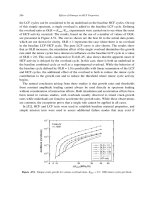
Figure
10
shows a profile of a
GaAs/AlGaAs
superlattice with and without sample
rotation. The profile without rotation shows a severe loss of depth resolution for the
aluminum and gallium signals after about 15 periods, whereas the profile with rota-
tion shows no significant loss
of
depth resolution after almost
70
periods. The data
708
PHYSICAL AND MAGNETIC PROPERTIES
Chapter
12
12
I
I
I
I
I I
a
Ga
GaA5/&.3G%.;As SUPERLAlTICE
v)
3
WITHOUT SAMPLE ROTATION
0
GaAs/Ab.3G%,,As SUPERLAlTICE
WITH SAMPLE ROTATION
I
I
I
I I
I
0
0.1
0.2
0.3
0.4
0.5 0.6
0.7
DEPTH
(pm)
0
Figure
10
SIMS
depth profiles with and without sample rotation during bombardment
by 3-keV
02+
at
40"
from normal incidence."
were taken using
a
3-keV oxygen primary
beam
rastered over
a
1
-mm
x
1
-mm
area
at
8
nm/ min. The rotation speed was approximately
0.6
cycles/ min. Additional
work by the same group has shown that the secondary ion yield changes described
above
are
removed
also
if the sample is rotated.
Related Articles in the Encyclopedia
Dynamic
SIMS,
AES,
SEM, STM, and
SFM
References
1
N. A. Burnham and
R
.J. Colton.
J.
fir.
Sci.
Zchnol.
A7,2906, 1989.
2
N. A. Burnham and
R
J. Colton. in
Scanning TunnelingMicroscopy: The-
ory
and Practice.
(D. A. Bonnell, ed.)
V.C.H.
Publishers, New York,
1991.
3
R.
D. Jacobson,
S.
R.
Wilson,
G.
A.
AI-Jumaily,
J.
R
McNeil, J. M. Ben-
nett,
and
L.
Mattsson.
Applied
Optics.
1991.
4
J.
R
McNeil,
et
al.
Optical
Eng.
26,953, 1987.
5
Ion
BombardmentModijkation ofsufaces
(0.
Auciello and
R.
Kelly, eds.)
Elsevier, Amsterdam,
19
84.
6
E
A. Stevie,
P
.M. Kahora,
D
.S.
Simons, and
l?
Chi.
/.
kc.
Sci.
Zchnol.
A6,76, 1988.
12.1
Surface
Roughness
709
7
R
M.
Bradley
and
J.
M. E.
Harper.
J
Vac.
Sci.
Tecbnol.
A6,2390,1988.
B
R.
G.
Wilson,
E
A.
Stevie, and
C.
W.
Magee.
Seconhry
Ion
Mas
Spectrom-
etry:
A
Practical Handbook
fir
Depth
Projling and Bulk
Impurity
Ana&.
Wiley,
New York,
1989.
s
A.
Zalar.
Tbin
Solid Film 124,223, 1983.
io
E H.
Cirlin,
J.
J.
Vajo,
T.
C.
Hasenberg,
and
R.
J.
Hauenstein.].
Vac.
Sci.
Zcbnol.
A8,4101,1990.
710
PHYSICAL AND MAGNETIC PROPERTIES
Chapter
12
12.2
Optical Scatterometry
JOHN
R.
MCNEIL, S.S.H. NAQVI, S.M. GASPAR,
K.C.
HICKMAN, AND
S.D.
WILSON
Contents
Introduction
Basic Principles and Applications
Comparison to Other Techniques
Conclusions
Introduction
Many technologies involve the need to monitor the surface topology of materials.
First the topology itself may be of direct interest. Second, topology is usually
strongly influenced by the processing steps used to produce the surface; characteriz-
ing the topology therefore
can
serve
as
a process monitor. Angle-resolved character-
ization of light scattered from a surface,
or
scatterometry, is a very attractive
diagnostic technique to characterize
a
sample’s topology. It is noncontact, nonde-
structive, rapid, and often provides quantitative data. Scatterometry can be used
as
a diagnostic tool in the fabrication
of
microelectronics, optoelectronics, optical ele-
ments, storage media, and other, less glamorous areas such
as
the production of
paper and rolled materials. Application
of
scatterometry in some
cases
eliminates
the need for microscopic examination. The technique is amenable to automated
processing, something which is not possible using microscopic examination.
Basic Principles and Applications
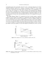
The arrangement illustrated in Figure
1
is commonly used
for
angular characreriza-
tion
of
scattered light. The light source is usually a laser. The incident beam may be
unpolarized,
or
it can be linearly polarized with provisions
for
rotating the plane of
polarization. Typically the plane of polarization is perpendicular
to
the plane
of
12.2
Optical Scatterometry
71
1
/r.
I
INCIDENT
BEAM
INCIDENT BEAM
NORMAL
1
I
IDETECTOR
TOR
SPECULARLY
BEAM
/
REFLECTED
b
Figure
1
Scatterometer arrangement, illustrating the geometry (a) and the experimen-
tal configuration
(b).
incidence (s-polarized light),
as
this avoids surface plasma wave coupling in con-
ducting samples. The laser output is spatially filtered
to
provide a well-defined spot
at the sample. This is critical for allowing measurements dose
to
the specularly
reflected beam or the directly transmitted beam (in the case of a sample which is
transmitting at the wavelength of interest); the significance is described below.
Sometimes the detector also has provisions for polarization discrimination. The
detector
is
typically a photomultiplier
or
a Si photodiode. Other detection arrange-
ments include multiple detectors
or
diode
arrays.
Arrangements that employ
cam-
712
PHYSICAL AND MAGNETIC PROPERTIES Chapter
12
era and screen configurations recently have shown utility for measuring scattering
in
two
dimensions. Theoretical aspects of light scattering are reviewed below in
connection with applications.
Applications of scatterometry can best be described by considering
two
general
categories of surfaces that are examined: surfaces which are nominally smooth, and
surfaces which are intentionally patterned. In the first category, scatterometry
is
used to measure surface roughness and other statistical properties
of
the sample’s
topology. Certain conditions of the surface are assumed, and these are discussed
below. In addition, for some “smooth” surfaces, such
as
optical components, the
scattered light intensity itself is the item of interest, and little
or
no additional inter-
pretation is needed. This information might be sufficient to predict the perfor-
mance of the sample, such
as
characterizing scattering
losses
from laser cavity
elements. Measuring
light
scattered from intentionally patterned surfaces is a
very convenient process monitor in manufacturing areas like microelectronics and
optoelectronics. This is an area of active research, with some results now appearing
in manufacturing
environment^.^-'
Smooth Surfaces: Surface
Topology
Characterization
The relation between scattering of electromagnetic radiation
and
surface topogra-
phy has been studied for many years, originally in connection with radar. In general
this relationship is complicated. However, the relation is simple in the case of a
clean, perfectly reflecting surface in which the heights of the surface irregularities
are much smaller than the wavelength of the scattered light (i.e., the smooth-surface
approximation). We present the results of Church’s treatment.*
Vector scattering theories describe the differential light scatter
dI,
as
where Cis a constant,
li
is the intensity of the incident light, and
do,
is the solid
angle of the detection system. The quantity Qin Equation
(l),
called the
opticdfac-
tor,
is independent of the surface condition and is a function of the angles of inci-
dence
(e+
$i),
the scattering angles
(e,
$,),
complex index of refraction
N
of the
surfice, and polarization states
of
the incident and scattered light,
xi
and
x,
respec-
tively. The
surfacefactor
P(p,q)
is the power spectral density
of
the surface rough-
ness; it is the output
of
the scatterometer measurement and is the function which
describes the surface structure.
If the surface (i.e., the best
fit
plane) is in the
x-y
plane, and
Z(x,y)
is the surface
height variation (surface roughness) relative to that plane, the power spectral den-
sity is given by
12.2
Optical
Scatterometry
713