Digital logic testing and simulation phần 7 pps
Bạn đang xem bản rút gọn của tài liệu. Xem và tải ngay bản đầy đủ của tài liệu tại đây (551.51 KB, 70 trang )
CONTROLLABILITY/OBSERVABILITY ANALYSIS
397
function will be difficult to control. In a similar vein, the observability of a node
depends on the elements through which its signals must propagate to reach an out-
put. Its observability can be no better than the observability of the elements through
which it must be driven. Therefore, before applying the SCOAP algorithm to a cir-
cuit, it is necessary to have, for each primitive that appears in a circuit, equations
expressing the 0- and 1-controllability of its output in terms of the controllability of
its inputs, and it is necessary to have equations that express the observability of each
input in terms of both the observability of that element and the controllability of
some or all of its other inputs.
Consider the three-input AND gate. To get a 1 on the output, all three inputs must
be set to 1. Hence, controllability of the output to a 1 state is a function of the con-
trollability of all three inputs. To produce a 0 on the output requires only that a sin-
gle input be at 0; thus there are three choices and, if there exists some quantitative
measure indicating the relative ease or difficulty of controlling each of these three
inputs, then it is reasonable to select the input that is easiest to control in order to
establish a 0 on the output. Therefore, the combinational 1- and 0-controllabilities,
CC
1
(
Y
) and
CC
0
(
Y
), of a three-input AND gate with inputs
X
1
,
X
2
and
X
3
and output
Y
can be defined as
CC
1
(
Y
) =
CC
1
(
X
1
) + CC
1
(X
2
) + CC
1
(X
3
) + 1
CC
0
(Y) = Min{CC
0
(X
1
), CC
0
(X
2
), CC
0
(X
3
)} + 1
Controllability to 1 is additive over all inputs and to 0 it is the minimum over all
inputs. In either case the result is incremented by 1 so that, for intermediate nodes,
the number reflects, at least in part, distance (measured in numbers of gates) to pri-
mary inputs and outputs. The controllability equations for any combinational func-
tion can be determined from either its truth table or its cover. If two or more inputs
must be controlled to 0 or 1 values in order to produce the value e, e ∈ {0,1}, then
the controllabilities of these inputs are summed and the result is incremented by 1. If
more than one input combination produces the value e, then the controllability num-
ber is the minimum over all such combinations.
Example For the two-input exclusive-OR the truth table is
The combinational controllability equations are
CC
0
(Y) = Min{CC
0
(X
1
) + CC
0
(X
2
), CC
1
(X
1
) + CC
1
(X
2
)} + 1
CC
1
(Y) = Min{CC
0
(X
1
) + CC
1
(X
2
), CC
1
(X
1
) + CC
0
(X
2
)} + 1
X
1
X
2
Y
000
011
101
110
398
DESIGN-FOR-TESTABILITY
The sequential 0- and 1-controllabilities for combinational circuits, denoted SC
0
and
SC
1
, are computed using similar equations.
Example For the two-input Exclusive-OR, the sequential controllabilities are:
SC
0
(Y) = Min{SC
0
(X
1
) + SC
0
(X
2
), SC
1
(X
1
) + SC
1
(X
2
)}
SC
1
(Y) = Min{SC
0
(X
1
) + SC
1
(X
2
), SC
1
(X
1
) + SC
0
(X
2
)}
When computing sequential controllabilities through combinational logic, the value
is not incremented. The intent of a sequential controllability number is to provide an
estimate of the number of time frames needed to provide a 0 or 1 at a given node.
Propagation through combinational logic does not affect the number of time frames.
When deriving equations for sequential circuits, both combinational and sequen-
tial controllabilities are computed, but the roles are reversed. The sequential control-
lability is incremented by 1, but an increment is not included in the combinational
controllability equation. The creation of equations for a sequential circuit will be
illustrated by means of an example.
Example Consider a positive edge triggered flip-flop with an active low reset but
without a set capability. Then, 0-controllability is computed with
CC
0
(Q) = Min{CC
0
(R), CC
1
(R) + CC
0
(D) + CC
0
(C) + CC
1
(C)}
SC
0
(Q) = Min{SC
0
(R), SC
1
(R) + SC
0
(D) + SC
0
(C) + SC
1
(C)} + 1
and 1-controllability is computed with
CC
1
(Q) = CC
1
(R) + CC
1
(D) + CC
0
(C) + CC
1
(C)
SC
1
(Q) = SC
1
(R) + SC
1
(D) + SC
0
(C) + SC
1
(C) + 1
The first two equations state that a 0 can be obtained on the output of the delay flip-
flop in either of two ways. It can be obtained either by setting the reset line to 0, or it
can be obtained by setting the reset line to 1, setting the data line to 0, and then cre-
ating a rising edge on the clock line. Since four events must occur in the second
choice, the controllability figure is the sum of the controllabilities of the four events.
The sequential equation is incremented by 1 to reflect the fact that an additional time
image is required to propagate a signal through the flip-flop. (This is not strictly true
since a reset will produce a 0 at the Q output in the same time frame.) A 1 can be
achieved only by clocking a 1 through the data line and that also requires holding
the reset line at a 1.
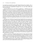
The Observability Equations The observability of a node is a function of
both the observability and the controllability of other nodes. This can be seen in
Figure 8.8. In order to observe the value at node P, it must be possible to observe the
CONTROLLABILITY/OBSERVABILITY ANALYSIS
399
Figure 8.8 Node observability.
value on node N. If the value on node N cannot be observed at the output of the circuit
and if node P has no other fanout, then clearly node P cannot be observed. However,
to observe node P it is also necessary to place nodes Q and R into the 1 state. There-
fore, a measure of the difficulty of observing node P can be computed with the fol-
lowing equation:
CO(P) = CO(N) + CC
1
(Q) + CC
1
(R) + 1
In general, the combinational observability of the output of a logic gate that drives
the input of an AND gate is equal to the observability of that AND gate input, which
in turn is equal to the sum of the observability of the AND gate output plus the 1-
controllabilities of its other inputs, incremented by 1.
For a more general primitive combinational function, the observability of a given
input can be computed from its propagation D-cubes (see Section 4.3.3). The pro-
cess is as follows:
1. Select those D-cubes that have a D or D
only on the input in question and 0, 1,
or X on all the other inputs.
2. For each cube, add the 0- and 1-controllabilities corresponding to each input
that has a 0 or 1 assigned.
3. Select the minimum controllability number computed over all the D-cubes
chosen and add to it the observability of the output.
Example Given an AND-OR-Invert described by the equation F = (A · B + C · D),
the propagation D-cubes for input A are (D, 1, 0, X) and (D, 1, X, 0). The combina-
tional observability for input A is equal to
CO(A) = Min{CO(Z) + CC
1
(B) + CC
0
(C),CO(Z) + CC
1
(B) + CC
0
(D)} + 1
The sequential observability equations, like the sequential controllability equa-
tions, are not incremented by 1 when computed through a combinational circuit. In
general, the sequential controllability/observability equations are incremented by 1
when computed through a sequential circuit, but the corresponding combinational
equations are not incremented.
P
Q
R
N
400
DESIGN-FOR-TESTABILITY
Example Observability equations will be developed for the Reset and Clock lines
of the delay flip-flop considered earlier. First consider the Reset line. Its observability
can be computed using the following equations:
CO(R) = CO(Q) + CC
1
(Q) + CC
0
(R)
SO(R) = SO(Q) + SC
1
(Q) + SC
0
(R) + 1
Observability equations for the clock are as follows:
CO(C) = Min{CO(Q) + CC
1
(Q) + CC
1
(R) + CC
0
(D) + CC
0
(C) + CC
1
(C),
CO(Q) + CC
0
(Q) + CC
1
(R) + CC
1
(D) + CC
0
(C) + CC
1
(C)}
SO(C) = Min{SO(Q) + CC
1
(Q) + SC
1
(R) + SC
0
(D) + SC
0
(C) + SC
1
(C),
SO(Q) + SC
0
(Q) + SC
1
(R) + SC
1
(D) + SC
0
(C) + SC
1
(C)} + 1
Equations for the Reset line of the flip-flop assert that observability is equal to the
sum of the observability of the Q output, plus the controllability of the flip-flop to a
1, plus the controllability of the Reset line to a 0. Expressed another way, the ability
to observe a value on the Reset line depends on the ability to observe the output of
the flip-flop, plus the ability to drive the flip-flop into the 1 state and then reset it.
Observability of the clock line is described similarly.
The Algorithm Since the equations for the observability of an input to a logic
gate or function depend on the controllabilities of the other inputs, it is necessary to
first compute the controllabilities. The first step is to assign initial values to all pri-
mary inputs, I, and internal nodes, N:
CC
0
(I)= CC
1
(I)= 1
CC
0
(N)= CC
1
(N)=
∞
SC
0
(I)= SC
1
(I)= 1
SC
0
(N)= SC
1
(N)=
∞
Having established initial values, each internal node can be selected in turn and the
controllability numbers computed for that node, working from primary inputs to pri-
mary outputs, and using the controllability equations developed for the primitives.
The process is repeated until, finally, the calculations stabilize. Node values must
eventually converge since controllability numbers are monotonically nonincreasing
integers.
Example The controllability numbers will be computed for the circuit of
Figure 8.9. The first step is to initially assign a controllability of 1 to all inputs and
∞
CONTROLLABILITY/OBSERVABILITY ANALYSIS
401
Figure 8.9 Controllability computations.
to all internal nodes. After the first iteration the 0- and 1-controllabilities of the inter-
nal nodes, in tabular form, are as follows:
After a second iteration the combinational 1-controllability of node 7 goes to a 4 and
the sequential controllability goes to 0. If the nodes had been rank-ordered—that is,
numbered according to the rule that no node is numbered until all its inputs are num-
bered—the second iteration would have been unnecessary.
With the controllability numbers established, it is now possible to compute the
observability numbers. The first step is to initialize all of the primary outputs, Y, and
internal nodes, N, with
CO(Y)= 0
SO(Y) = 0
CO(N)=
∞
SO(N)=
∞
Then select each node in turn and compute the observability of that node. Continue
until the numbers converge to stable values. As with the controllability numbers,
observability numbers must eventually converge. They will usually converge much
more quickly, with the fewest number of iterations, if nodes closest to the outputs
are selected first and those closest to the inputs are selected last.
NCC
0
(N) CC
1
(N) SC
0
(N) SC
1
(N)
62 3 0 0
72
∞
0
∞
82 3 0 0
92 2 0 0
10 7 4 0 0
R
1
2
3
4
5
6
7
8
9
10
402
DESIGN-FOR-TESTABILITY
Example The observability numbers will now be computed for the circuit of
Figure 8.9. After the first iteration the following table is obtained:
On the second iteration the combinational and sequential observabilities of node 9
settle at 7 and 0, respectively.
SCOAP can be generalized using the D-algorithm notation (cf. Section 4.3.1).
This will be illustrated using the truth table for the arbitrary function defined in
Figure 8.10. In practice, this might be a frequently used primitive in a library of
macrocells. The first step is to define the sets P
1
and P
0
. Then create the intersection
P
1
∩ P
0
and use the resulting intersections, along with the truth table, to create con-
trollability and observability equations. The sets P
1
and P
0
are as follows:
P
1
= {(0,0,0), (0,1,0), (1,0,1), (1,1,0)} = {(0,x,0), (1,0,1), (x,1,0)}
P
0
= {(0,0,1), (0,1,1), (1,0,0), (1,1,1)} = {(0,x,1), (1,0,0), (x,1,1)}
The intersection table P
1
∩ P
0
is as follows:
N CO(N) SO(N)
9
∞∞
85 0
75 0
65 0
57 0
47 0
38 0
27 0
17 0
ABCZ
00DD
D
00D
01DD
D01 D
10DD
1D
1D
1D0D
11DD
1 x D D
x 1DD
CONTROLLABILITY/OBSERVABILITY ANALYSIS
403
Figure 8.10 Truth table for arbitrary function.
Note first that some members of P
1
and P
0
were left out of the intersection table. The
rows that were omitted were those that had either two or three D and/or D
signals as
inputs. This follows from the fact that SCOAP does not compute observability
through multiple inputs to a function. Note also that three rows were crossed out and
two additional rows were added at the bottom of the intersection table. The first of
these added rows resulted from the intersection of rows 1 and 3. In words, it states
that if input A is a 1, then the value at input C is observable at Z regardless of the
value on input B. The second added row results from the intersection of rows 3 and
8. The following controllability and observability equations for this function are
derived from P
0
, P
1
, and their intersection:
CO(A) = min{CC
0
(B) + CC
0
(C), CC
0
(B) + CC
1
(C)} + CO(Z) + 1
CO(B) = min{CC
1
(A) + CC
1
(C), CC
1
(A) + CC
0
(C)} + CO(Z) + 1
CO(A) = min{CC
0
(A), CC
1
(A) + CC
0
(B),CC
1
(B)} + CO(Z) + 1
CC
0
(Z) = min{CC
0
(A) + CC
1
(C), CC
1
(A) + CC
0
(B) + CC
0
(C),CC
1
(B) + CC
1
(C)} + 1
CC
1
(Z) = min{CC
0
(A) + CC
0
(C), CC
1
(A) + CC
0
(B) + CC
1
(C),CC
1
(B) + CC
0
(C)} + 1
8.3.2 Other Testability Measures
Other algorithms exist, similar to SCOAP, which place different emphasis on cir-
cuit parameters. COP (controllability and observability program) computes con-
trollability numbers based on the number of inputs that must be controlled in order
to establish a value at a node.
3
The numbers therefore do not reflect the number of
levels of logic between the node being processed and the primary inputs. The
SCOAP numbers, which encompass both the number of levels of logic and the
number of primary inputs affecting the C/O numbers for a node, are likely to give a
more accurate estimate of the amount of work that an ATPG must perform. How-
ever, the number of primary inputs affecting C/O numbers perhaps reflects more
0
0
0
0
1
1
1
1
A
0
0
1
1
0
1
0
1
C
1
1
0
0
0
1
1
0
ZB
0
0
1
1
0
0
1
1
404
DESIGN-FOR-TESTABILITY
accurately the probability that a node will be switched to some value randomly;
hence it may be that it more closely correlates with the probability of random fault
coverage when simulating test vectors.
Testability analysis has been extended to functional level primitives. FUNTAP
(functional testability analysis program)
4
takes advantage of structures such as n-
wide data paths. Whereas the single net may have binary values 0 and 1, and these
values can have different C/O numbers, the n-wide data path made up of binary sig-
nals may have a value ranging from 0 to 2
n
– 1. In FUNTAP no significance is
attached to these values; it is assumed that the data path can be set to any value i,
0 ≤ i ≤ 2
n
− 1, with equal ease or difficulty. Therefore, a single controllability number
and a single observability number are assigned to all nets in a data path, independent
of the logic values assigned to individual nets that make up the data path.
The ITTAP program
5
computes controllability and observability numbers, but, in
addition, it computes parameters TL0, TL1, and TLOBS, which measure the length
of the sequence needed in sequential logic to set a net to 0 or 1 or to observe the
value on that node. For example, if a delay flip-flop has a reset that can be used to
reset the flip-flop to 0, but can only get a 1 by clocking it in from the Data input, then
TL0 = 1 and TL1 = 2.
A more significant feature of ITTAP is its selective trace capability. This feature
is based on two observations. First, controllabilities must be computed before
observabilities, and second, if the numbers were once computed, and if a change is
made to enhance testability, numbers need only be recomputed for those nodes
where the numbers can change. The selection of elements for recomputation is simi-
lar to event-driven simulation. If the controllability of a node changes because of the
addition of a test point, then elements driven by that element must have their con-
trollabilities recomputed. This continues until primary outputs are reached or ele-
ments are reached where the controllability numbers at the outputs are unaffected by
changing numbers at the inputs. At that point, the observabilities are computed back
toward the inputs for those elements with changed controllability numbers on their
inputs.
The use of selective trace provides a savings in CPU time of 90–98% compared
to the time required to recompute all numbers in a given circuit. This makes it ideal
for use in an interactive environment. The designer visually inspects either a circuit
or a list of nodes at a video display terminal and then assigns a test point and imme-
diately views the results. Because of the quick response, the test point can be shifted
to other nodes and the numbers recomputed. After several such iterations, the logic
designer can settle on the node that provides the greatest improvement in the C/O
numbers.
The interactive strategy has pedagogical value. Placing a test point at a node with
the worst C/O numbers is not always the best solution. It may be more effective to
place a test point at a node that controls the node in question, since this may improve
controllability of several nodes. Also, since observability is a function of controlla-
bility, greatest improvements in testability may sometimes be had by assigning a test
point as an input to a gate rather than as an output, even though the analysis program
indicates that the observability is poor. The engineer who uses the interactive tool,
CONTROLLABILITY/OBSERVABILITY ANALYSIS
405
particularly recent graduates who may not have given much thought to testability
issues, may learn with such an interactive tool how best to design for testability.
8.3.3 Test Measure Effectiveness
Studies have been conducted to determine the effectiveness of testability analysis.
Consider the circuit defined by the equation
F = A·(B + C + D)
An implementation can be realized by a two-input AND gate and a three-input OR
gate. With four inputs, there are 16 possible combinations on the inputs. An SA1 fault
on input A to the AND gate has a 7/16 probability of detection, whereas an SA0 on
any input to the OR gate has a 1/16 probability of detection. Hence a randomly gener-
ated 4-bit vector applied to the inputs of the circuit is seven times as likely to detect
the fault on the AND gate input as it is to detect a fault on a particular OR gate input.
Suppose controllability of a fault is defined as the fraction of input vectors that set a
faulty net to a value opposite its stuck-at value, and observability is defined as the
fraction of input vectors that propagate the fault effect to an output.
6
Testability is then
defined as the fraction of input vectors that test the fault. Obviously, to test a fault, it is
necessary to both control and observe the fault effect; hence testability for a given fault
can be viewed as the number of vectors in the intersection of the controllability and
observability sets, divided by the total number of vectors. But, there may be two reason-
ably large sets whose intersection is empty. A simple example is shown in Figure 8.11.
The controllability for the bottom input of gate numbered 1 is 1/2. The observability is
1/4. Yet, the SA1 on the input cannot be detected because it is redundant.
In another investigation of testability measures, the authors attempt to determine
a relationship between testability figures and detectability of a fault.
7
They parti-
tioned faults into classes based on testability estimates for the faults and then plotted
curves of fault coverage versus vector number for each of these classes. The curves
were reasonably well behaved, the fault coverage curves rising more slowly, in gen-
eral, for the more difficult to test fault classes, although occasionally a curve for
some particular class would rise more rapidly than the curve for a supposedly easier
to test class of faults. They concluded that testability data were a poor predictor of
fault detection for individual faults but that general information at the circuit level
was available and useful. Furthermore, if some percentage, say 70%, of a class of
difficult to test faults are tested, then any fixes made to the circuit for testability pur-
poses have only a 30% chance of being effective.
Figure 8.11 An undetectable fault.
1
3
B
A
2
406
DESIGN-FOR-TESTABILITY
8.3.4 Using the Test Pattern Generator
If test vectors for a circuit are to be generated by an ATPG, then the most direct way
in which to determine its testability is to simply run the ATPG on the circuit. The
ability (or inability) of an ATPG to generate tests for all or part of a design is the best
criterion for testability. Furthermore, it is a good practice to run test pattern genera-
tion on a design before the circuit has been fabricated. After a board or IC has been
fabricated, the cost of incorporating changes to improve testability increases
dramatically.
A technique employed by at least one commercial ATPG employs a preprocess
mode in which it attempts to set latches and flip-flops to both the 0 and 1 state before
attempting to create tests for specific faults in a circuit.
8
The objective is to find trou-
blesome circuits before going into test pattern generation mode. The ATPG compiles
a list of those flip-flops for which it could not establish the 0 and/or 1 state. When-
ever possible, it indicates the reason for the failure to establish desired value(s). The
failure may result from such things as races in which relative timing of the signals is
too close to call with confidence, or it could be caused by bus conflicts resulting from
inability to set one or more tri-state control lines to a desired value. It could also be
the case that controllability to 0 or 1 of a flip-flop depends on the value of another
flip-flop that could not be controlled to a critical value. It also has criteria for deter-
mining whether the establishment of a 0 or 1 state took an excessive amount of time.
Analysis of information in the preprocess mode may reveal clusters of nodes that
are all affected by a single uncontrollable node. It is also important to bear in mind
that nodes which require a great deal of time to initialize can be as detrimental to
testability as nodes that cannot be initialized. An ATPG may set arbitrary limits on
the amount of time to be expended in trying to set up a test for a particular fault.
When that threshold is exceeded, the ATPG will give up on the fault even though a
test may exist.
C/O numbers can be used by the ATPG to influence the decision-making process.
On average, this can significantly reduce the amount of time required to create test
patterns. The C/O numbers can be attached to the nodes in the circuit model, or the
numbers can be used to rearrange the connectivity tables used by the ATPG, so that
the ATPG always tries to propagate or justify the easiest to control or observe signals
first. Initially, when a circuit model is read into the ATPG, connectivity tables are
constructed reflecting the interconnections between the various elements in the cir-
cuit. A FROM table lists the inputs to an element, and a TO table lists the elements
driven by a particular element.
By reading observability information, the ATPG can sort the elements in the TO
table so that the most observable path is selected first when propagating elements.
Likewise, when justifying logic values, controllability information can be used to
select the most controllable input to the gate. For example, when processing an
AND gate, if it is necessary to justify a 0 on the output of the AND gate, then the
input with the lowest 0-controllability should be tried first. If it cannot be justified,
then attempt the other inputs, always selecting as the next choice the input, not yet
attempted, that is judged to be most controllable.
THE SCAN PATH
407
8.4 THE SCAN PATH
Ad hoc DFT methods can be useful in small circuits that have high yield, as well as
circuits with low sequential complexity. For ICs on small die with low gate count, it
may be necessary to get only a small boost in fault coverage in order to achieve
required AQL, and one or more ad hoc DFT solutions may be adequate. However, a
growing number of design starts are in the multi-million transistor range. Even if it
were possible to create a test with high-fault coverage, it would in all likelihood take
an unacceptably long time on a tester to apply the test to an IC. However, it is sel-
dom the case that an adequate test can be created for extremely complex devices
using traditional methods. In addition to the length of the test, test development cost
continues to grow. Another factor of growing importance is customer expectations.
As digital products become more pervasive, they increasingly are purchased by cus-
tomers unsympathetic to the difficulties of testing, they just want the product to
work. Hence, it is becoming imperative that devices be free of defects when shipped
to customers.
The aforementioned factors increase the pressure on vendors to produce fault-
free products. The ever-shrinking feature sizes of ICs simultaneously present both a
problem and an opportunity for vendors. The shrinking feature sizes make the die
susceptible to defects that might not have affected it in a previous generation of
technology. On the other hand, it affords an opportunity to incorporate more test
related features on the die. Where die were once core-limited, now the die are more
likely to be pad-limited (cf. Figure 8.12). In core-limited die there may not be suffi-
cient real estate on the die for all the features desired by marketing; as a result, test-
ability was often the first casualty in the battle for die real estate. With pad-limited
die, larger and more complex circuits, and growing test costs, the argument for more
die real estate dedicated to test is easier to sell to management.
8.4.1 Overview
Before examining scan test, consider briefly the circuit of Problem 8.10, an eight-
state sequential circuit implemented as a muxed state machine. It is fairly easy to
generate a complete test for the circuit because it is a completely specified state
machine (CSSM); that is, every state defined by the flip-flops can be reached from
some other state in one or more transitions. Nonetheless, generating a test program
Figure 8.12 The changing face of IC design.
Core-limited die Pad-limited die
408
DESIGN-FOR-TESTABILITY
becomes quite tedious because of all the details that must be maintained while prop-
agating and justifying logic assignments through the time and logic dimensions. The
task becomes orders of magnitude more difficult when the state machine is imple-
mented using one-hot encoding. In that design style, every state is represented by a
unique flip-flop, and the circuit becomes an incompletely specified state machine
(ISSM)—that is, one in which n flip-flops implement n legal states out of 2
n
possible
states. Backtracing and justifying logic values in the circuit becomes virtually
impossible.
Regardless of how the circuit is implemented, with three or eight flip-flops, the
test generation task for a fault in combinational logic becomes much easier if it
were possible to compute the required test values at the I/O pins and flip-flops,
and then load the required values directly into the flip-flops without requiring sev-
eral vectors to transition to the desired state. The scan path serves this purpose. In
this approach the flip-flops are designed to operate either in parallel load or serial
shift mode. In operational mode the flip-flops are configured for parallel load.
During test the flip-flops are configured for serial shift mode. In serial shift mode,
logic values are loaded by serially shifting in the desired values. In similar fash-
ion, any values present in the flip-flops can be observed by serially clocking out
their contents.
A simple means for creating the scan path consists of placing a multiplexer just
ahead of each flip-flop as illustrated in Figure 8.13. One input to the 2-to-1 multi-
plexer is driven by normal operational data while the other input—with one excep-
tion—is driven by the output of another flip-flop. At one of the multiplexers the
serial input is connected to a primary input pin. Likewise, one of the flip-flop outputs
is connected to a primary output pin. The multiplexer control line, also connected to
a primary input pin, is now a mode control; it can permit parallel load for normal
operation or it can select serial shift in order to enter scan mode. When scan mode is
selected, there is a complete serial shift path from an input pin to an output pin.
Since it is possible to load arbitrary values into flip-flops and read the contents
directly out through the serial shift path, ATPG requirements are enormously simpli-
fied. The payoff is that the complexity of testing is significantly reduced because it
is no longer necessary to propagate tests through the time dimension represented by
sequential circuits. The scan path can be tested by shifting a special pattern through
Figure 8.13 A scan path.
MUX MUX
Register Register
Out 1 Out 2
Select
Scan in
Data 2Data 1
MUX
Register
Scan out
Data N
Out N
THE SCAN PATH
409
the scan path before even beginning to address stuck-at faults in the combinational
logic. A test pattern consisting of alternating pairs of 1s and 0s (i.e., 11001100 )
will test the ability of the scan path to shift all possible transitions. This makes it
possible for the ATPG to ignore faults inside the flip-flops, as well as stuck-at faults
on the clock circuits.
During the generation of test patterns, the ATPG treats the flip-flops as I/O
pins. A flip-flop output appears to be a combinational logic input, whereas a flip-
flop input appears to be a combinational logic output. When an ATPG is propagat-
ing a sensitized path, it stops at a flip-flop input just as it would stop at a primary
output. When justifying logic assignments, the ATPG stops at the output of flip-
flops just as it would stop at primary inputs. The only difference between the
actual I/O pins and flip-flop “I/O pins” is the fact that values on the flip-flops must
be serially shifted in when used as inputs and serially shifted out when used as
outputs.
When a circuit with scan path is used in its normal mode, the mode control, or
test control, is set for parallel load. The multiplexer selects normal operational data
and, except for the delay through the multiplexer, the scan circuitry is transparent.
When the device is being tested, the mode control alternates between parallel load
and serial shift. This is illustrated in Figure 8.14.
The figure assumes a circuit composed of four scan-flops that, during normal
mode, are controlled by positive clock edges. Data are serially shifted into the
scan path when the scan-enable is high. After all of the scan-flops are loaded,
the scan-enable goes low. At this point the next clock pulse causes normal cir-
cuit operation using the data that were serially shifted into the scan-flops. That
data pass through the combinational logic and produce a response that is
clocked into destination scan-flops. Note that data present at the scan-input are
ignored during this clock period. After one functional clock has been applied,
scan-enable again becomes active. Now the Clk signal again loads the scan-
flops. During this operation, response data are also captured at the scan-out pin.
That data are compared to expected data to determine whether or not any faults
are present in the circuit.
The use of scan tremendously simplifies the task of creating test stimuli for
sequential circuits, since the circuit is essentially reduced to a combinational ATPG
for test purposes, and algorithms for those circuits are well understood, as we saw
in Chapter 4. It is possible to achieve very high fault coverage, often in the range of
Figure 8.14 Scan shift operation.
Clk
SI
1
SI
2
SI
3
SI
4
X
SI
1
SI
2
SI
3
SI
4
scan-input
scan-enable
scan-out
X
SO
1
SO
2
SO
3
SO
4
SO
1
SO
3
SO
2
SO
4
410
DESIGN-FOR-TESTABILITY
Figure 8.15 Scan flip-flop symbol.
97–99% for the parts of the circuit that can be tested with scan. Equally important
for management, the amount of time required to generate the test patterns and
achieve a target fault coverage is predictable. Scan can also help to reduce time on
the tester since, as we shall see, multiple scan paths can run in parallel. However,
it does impose a cost. The multiplexers and the additional metal runs needed to
connect the mode select to the flip-flops can require from 5% to 20% of the real
estate on an IC. The performance delay introduced by the multiplexers in front of
the flip-flops may impose a penalty of from 5% to 10%, depending on the depth of
the logic.
8.4.2 Types of Scan-Flops
The simplest form of scan-flop incorporates a multiplexer into a macrocell together
with a delay flip-flop. A common symbol denoting a scan-flop is illustrated in
Figure 8.15. Operational data enter at D, while scan data enter at SI. The scan
enable, SE, determines which data are selected and clocked into the flip-flop.
Dual Clock Serial Scan An implementation of scan with dual clocks is shown
in Figure 8.16.
9
In this implementation, comprised of CMOS transmission gates, the
goal was to have the least possible impact on circuit performance and area overhead.
Figure 8.16 Flip-flop with dual clock.
QD
SI
SE
CK
R
D
SI
Dclk
Sclk
Q
SO_L
Dclk
Sclk
Master
Slave
Scan slave
Jam latch
THE SCAN PATH
411
Dclk is used in operational mode, and Sclk is the scan clock. Operational data and
scan data are multiplexed using Dclk and Sclk. When operating in scan mode, Dclk
is held high and Sclk goes low to permit scan data to pass into the Master latch.
Because Dclk is high, the scan data pass through the Slave latch and, when Sclk
goes high, pass through the Scan slave and appears at SO_L.
Addressable Registers Improved controllability and observability of sequen-
tial elements can be obtained through the use of addressable registers.
10
Although,
strictly speaking, not a scan or serial shift operation, the intent is the same—that is,
to gain access and control of sequential storage elements in a circuit. This approach
uses X and Y address lines, as illustrated in Figure 8.17. Each latch has an X and Y
address, as well as clear and preset inputs, in addition to the usual clock and data
lines. A scan address goes to X and Y decoders for the purpose of generating the X
and Y signals that select a latch to be loaded. A latch is forced to a 1 (0) by setting
the address lines and then pulsing the Preset (Clear) line.
Readout of data is also accomplished by means of the X and Y addresses. The
selected element is gated to the SDO (Serial Data Out) pin, where it can be
observed. If there are more address lines decoded than are necessary to observe
latches, the extra X and Y addresses can be used to observe nodes in combinational
logic. The node to be observed is input to a NAND gate along with X and Y signals,
as a latch would be; when selected, its value appears at the SDO.
The addressable latches require just a few gates for each storage element. Their
affect on operation during normal operation is negligible, due mainly to loading
caused by the NAND gate attached to the Q output. The scan address could require
several I/O pins, but it could also be generated internally by a counter that is initially
reset and then clocked through consecutive addresses to permit loading or reading of
the latches.
Random access scan is attractive because of its negligible effect on IC perfor-
mance and real estate. It was developed by a mainframe company where perfor-
mance, rather than die area, was the overriding issue. Note, however, that with
shrinking component size the amount of area taken by interconnections inside an IC
grows more significant; the interconnect represents a larger percentage of total chip
Figure 8.17 Addressable flip-flop.
Data
Clock
Clear
Preset
X
Y
Q
SDO
412
DESIGN-FOR-TESTABILITY
area. The addressable latches require that several signal lines be routed to each
addressable latch, and the chip area occupied by these signal lines becomes a major
factor when assessing the cost versus benefits of the various methods.
8.4.3 Level-Sensitive Scan Design
Much of what is published about DFT techniques is not new. They have been
described as early as December 1963
11
and again in April 1964.
12
Detailed descrip-
tion of a scan path and its proposed use for testability and operational modes is
described in a patent filed in 1968.
13
Discussion of scan path and derivation of a for-
mal cost model were published in 1973.
14
The level-sensitive scan design (LSSD)
methodology was introduced in a series of papers presented at the Design Automa-
tion Conference in 1977.
15 –17
LSSD extends DFT beyond the scan concept. It augments the scan path with addi-
tional rules whose purpose is to cause a design to become level sensitive. A level-sen-
sitive system is one in which the steady-state response to any allowed input state
change is independent of circuit and wire delays within the system. In addition, if an
input state change affects more than one input signal, then the response must be inde-
pendent of the order in which they change.
15
The object of these rules is to preclude
the creation of designs in which correct operation depends on critical timing factors.
To achieve this objective, the memory devices used in the design are level-sensitive
latches. These latches permit a change of internal state at any time when the clock is
in one state, usually the high state, and inhibit state changes when the clock is in the
opposite state. Unlike edge-sensitive flip-flops, the latches are insensitive to rising and
falling edges of pulses, and therefore the designer cannot create circuits in which cor-
rect operation depends on pulses that are themselves critically dependent on circuit
delay. The only timing that must be taken into account is the total propagation time
through combinational logic between the latches.
In the LSSD environment, latches are used in pairs as illustrated in Figure 8.18.
These latch pairs are called shift-register latches (SRL), and their operation is con-
trolled by multiple clocks, denoted A, B, and C. The Data input is used in opera-
tional mode whereas Scan-in, which is driven by the L2 output of another SRL, is
used in the scan mode. During operational mode the A clock is inactive. The C clock
is used to clock data into L1 from the Data input, and output can be taken from
either L1 or L2. If output is taken from L2, then two clock signals are required. The
second signal, called the B clock, clocks data into L2 from the L1 latch. This config-
uration is sometimes referred to as a double latch design.
When the scan path is used for testing purposes, the A clock is used in conjunc-
tion with the B clock. Since the A clock causes data at the Scan-in input to be latched
into L1, and the Scan-in signal comes from the L2 output of another SRL (or a pri-
mary input pin), alternately switching the A and B clocks serially shifts data through
the scan path from the Scan-in terminal to the Scan-out terminal.
Conceptually, LSSD behaves much like the dual-clock configuration discussed
earlier. However, there is more to LSSD, namely, a set of rules governing the man-
ner in which logic is clocked. Consider the circuit depicted in Figure 8.19. If S1, S2,
THE SCAN PATH
413
Figure 8.18 The shift register latch.
and S3 are L1 latches, the correct operation of the circuit depends on relative timing
between the clock and data signals. When the clock is high, there is a direct combi-
national logic path from the input of S1 to the output of S3. Since the clock signal
must stay high for some minimum period of time in order to latch the data, this
direct combinational path will exist for that duration.
In addition, the signal from S1 to S2 may go through a very short propagation
path. If the clock does not drop in time, input data to the S1 latch may not only get
Figure 8.19 Some timing problems.
L1
L2
Data
C
Scan-in
A
B
Scan-in
Data
C
A
B
L1
L2
S1 S2 S3
Combinational
logic
Combinational
logic
A
B
C
414
DESIGN-FOR-TESTABILITY
latched in S1 but may reach S2 and get latched into S2 a clock period earlier than
intended. Hence, as illustrated in waveform A the short propagation path can cause
unpredictable results. Waveform C illustrates the opposite problem. The next clock
pulse appears before new data reaches S2. Clearly, for correct behavior it is neces-
sary that the clock cycle be as short as possible, but it must not be shorter than the
propagation time through combinational logic.
The use of the double latch design can eliminate the situation in waveform A.
To resolve this problem, LSSD imposes restrictions on the clocking of latches.
The rules will be listed and then their effect on the circuit of Figure 8.19 will be
discussed.
1. Latches are controlled by two or more nonoverlapping clocks such that a latch
X may feed the data port of another latch Y if and only if the clock that sets the
data into latch Y does not clock latch X.
2. A latch X may gate a clock C
1
to produce a gated clock C
2
that drives another
latch Y if and only if clock C
3
does not clock latch X, where C
3
is any clock
produced from C
1
.
3. It must be possible to identify a set of clock primary inputs from which the
clock inputs to SRLs are controlled either through simple powering trees or
through logic that is gated by SRLs and/or nonclock primary inputs.
4. All clock inputs to all SRLs must be at their off states when all clock primary
inputs are held to their off states.
5. The clock signal that appears at any clock input of an SRL must be controlled
from one or more clock primary inputs such that it is possible to set the clock
input of the SRL to an on state by turning any one of the corresponding pri-
mary inputs to its on state and also setting the required gating condition from
SRLs and/or nonclock primary inputs.
6. No clock can be ANDed with the true value or complement value of another
clock.
7. Clock primary inputs may not feed the data inputs to latches, either directly or
through combinational logic, but may only feed the clock input to the latches
or the primary outputs.
Rule 1 forbids the configuration shown in Figure 8.19. A simply way to comply
with the rules is to use both the L1 and L2 latches and control them with nonover-
lapping clocks as shown in Figure 8.20. Then the situation illustrated in waveform A
will not occur. The contents of the L2 latch cannot change in response to new data at
its input as long as the B clock remains low. Therefore, the new data entering the L1
latch of SRL S1, as a result of clock C being high, cannot get through its L2 latch,
because the B clock is low and hence cannot reach the input of SRL S2. The input to
S2 remains stable and is latched by the C clock.
The use of nonoverlapping clocks will protect a design from problems caused by
short propagation paths. However, the time between the fall of clock C and the rise
THE SCAN PATH
415
Figure 8.20 The two-clock signal.
of clock B is “dead time”; that is, once the data are latched into L1, the goal is to
move it into L2 as quickly as possible in order to realize maximum performance.
Thus, the interval from the fall of C to the rise of B in Figure 8.20 should be as brief
as possible without, however, making the duration too short. In a chip with a great
many wire paths, the two clocks may be nonoverlapping at the I/O pins and yet may
overlap at one or more SRLs inside the chip due to signal path delays. This condi-
tion is referred to as clock skew. When debugging a design, experimentation with
clock edge separation can help to determine whether clock skew is causing prob-
lems. If clock skew problems exist, it may be necessary to change the layout of a
chip or board, or it may require a greater separation of clock edges to resolve the
problem.
The designer must still be concerned with the configuration in waveform C; that
is, the clock cycle must exceed the propagation delay of the longest propagation
path. However, it is a relatively straightforward task to compute propagation delays
along combinational logic paths. Timing verification, as described in Section 2.13,
can be used to compute the delay along each path and then print out all critical paths
that exceed a specified threshold. The design team can elect to redesign the critical
paths or increase the clock cycle.
Test program development using the LSSD scan path closely follows the tech-
nique used with other scan paths. One interesting variant when testing is the fact that
the scan path itself can be checked with what is called a flush test.
16
In a flush test the
A and B clocks are both set high. This creates a direct combinational path from the
scan-in to the scan-out. It is then possible to apply a logic 1 and 0 to the scan-in and
observe them directly at the scan output without further exercising the clocks. This
flush test exercises a significant portion of the scan path. The flush test is followed by
clocking 1s and 0s through the scan path to ensure that the clock lines are fault-free.
Another significant feature of LSSD, as implemented, is the fact that it is sup-
ported by a design automation system that enforces the design rules.
17
Since the
design automation system incorporates much knowledge of LSSD, it is possible to
check the design for compliance with design rules. Violations detected by the check-
ing programs can be corrected before the design is fabricated, thus ensuring that
design violations will not compromise the testability goals that were the object of
the LSSD rules.
The other DFT approaches discussed, including non-LSSD scan and addressable
registers, do not, in and of themselves, inhibit some design practices that traditionally
C
B
416
DESIGN-FOR-TESTABILITY
have caused problems for ATPGs. They require design discipline imposed either by
the logic designers or by some designated testability supervisor. LSSD, by requiring
that designs be entered into a design data base via design automation programs that
can check for rule violations, makes it difficult to incorporate design violations with-
out concurrence of the very people who are ultimately responsible for testing the
design.
8.4.4 Scan Compliance
The intent of scan is to make a circuit testable by causing it to appear to be strictly
combinational to an ATPG. However, not all circuits can be directly transformed
into combinational circuits by adding a scan path. Consider the self-resetting flip-
flop in Figure 8.21. Any attempt to serially shift data through the scan-in (SI) will be
defeated by the self-resetting capability of flip-flop S
2
. The self-resetting capability
not only forces S
2
back to the 0 state, but the effect on S
3
, as data are scanned
through, is unpredictable. Whether or not scan data reach S
3
from S
2
will depend on
the value of the Delay as well as the period of the clock.
A number of other circuit configurations create similar complications. This
includes configurations such as asynchronous set and clear inputs and flip-flops
whose clock, set, and/or clear inputs are driven by combinational logic. Two prob-
lems result when flip-flops are clocked by derived clocks—that is, clocks generated
from subcircuits whose inputs are other clocks and random logic signals. The first of
these problems is that an ATPG may have difficulty creating the clocking signal and
keeping it in proper synchronization with clock signals on other flip-flops. The other
problem is the fact that the derived clock may be glitchy due to races and hazards.
So, although the circuit may work correctly during normal operation, test vectors
generated by an ATPG may create input combinations not intended by the designers
of the circuit and, as a result, the circuit experiences races and hazards that do not
occur during normal operation.
Latches are forbidden by some commercial systems that support scan. Scan-
based ATPG tools expect the circuit they are processing to be a pure combinational
circuit. Since the latches hold state information, logic values emanating from the
latches are unpredictable. Therefore, those values will be treated as Xs. This can
cause a considerable amount of logic to become untestable. One way to implement
Figure 8.21 A reset problem.
Delay
Mode
Serial-in
QD
SI
SE
CK
R
QD
SI
SE
CK
Q
QD
SI
SE
CK
R
S
1
S
2
S
3
THE SCAN PATH
417
testable latches is shown in Figure 8.22.
18
When in test mode, the TestEnable signal
is held fixed at 1, thus blocking the feedback signals. As a result, the NAND gates
appear, for purposes of test, to be inverters. A slight drawback is that some faults
become undetectable. But this is preferable to propagating Xs throughout a large
block of combinational logic.
If there are D latches present in the circuit—that is, those with Data and Enable
inputs—then a TestEnable signal can be ORed with the Enable signal. The TestEnable
signal can be held at logic 1 during test so that the D latch appears, for test purposes,
to be a buffer or inverter.
Many scan violations can be resolved through the use of multiplexers. For exam-
ple, if a circuit contains a combinational feedback loop, then a multiplexer can be
used to break up the loop. This was illustrated in Figure 8.3 where the configuration
was used to avoid gating the clock signal. To use this configuration for test, the Load
signal selects the feedback loop during normal operation, but selects a test input sig-
nal during test. The test input can be driven by a flip-flop that is included in the scan
chain but is dedicated to test, that is, the flip-flop is not used during normal opera-
tion. This circuit configuration may require two multiplexers; One is used to select
between Load and Data, and the second one is used to choose between scan-in and
normal operation.
Tri-state circuits can cause problems because they are often used when two or
more devices are connected to a bus. When several drivers are connected to a bus, it
is sometimes the case that none of the drivers are active, causing the bus to enter the
unknown state. When that occurs, the X on the bus may spread throughout much of
the logic, thus rendering a great deal of logic untestable for those vectors when the
bus is unknown.
One way to prevent conflicts at buses with multiple drivers is to use multiplexers
rather than tri-state drivers. Then, if there are no signals actively driving the bus, it
can be made to default to either 0 or 1. If tri-state drivers are used, a 1-of-n selector
can be used to control the tri-state devices. If the number of bus drivers n is 2
d− 1
< n
< 2
d
, there will be combinations of the 2
d
possible selections for which no signal is
driving the bus. The unused combinations can be set to force 0s or 1s onto the bus.
This is illustrated in Figure 8.23, where d = 2, and one of the four bus drivers is con-
nected to ground. If select lines S
1
and S
2
do not choose any of D
1
, D
2
, or D
3
, then
the Bus gets a logic 0. Note that while the solution in Figure 8.23 maintains the bus
at a known value regardless of the values of S
1
and S
2
, a fault on a tri-state enable
line can cause the faulty bus to assume an indeterminate value, resulting in at best a
Figure 8.22 Testable NAND latch.
Q
Q
Q
Q
S
R
S
R
TestEnable
418
DESIGN-FOR-TESTABILITY
Figure 8.23 Forcing a bus to a known value.
probable detect. When a multiplexer is used, both good and faulty circuits will have
known, but different, values.
A potentially more serious situation occurs if a circuit is designed in such a way
that two or more drivers may be simultaneously active during scan test. For exam-
ple, the tri-state enables may be driven, directly or indirectly, by flip-flops. If two or
more drivers are caused to become active during scan and if they are attempting to
drive the circuit to opposite values, the test can damage the very circuit it is
attempting to evaluate for correct operation.
8.4.5 Scan-Testing Circuits with Memory
With shrinking feature sizes, increasing numbers of ICs are being designed with
memory on the same die with random logic. Memory often takes up 80% or more of
the transistors on a die in microprocessor designs while occupying less than half the
die area (cf. Section 10.1). Combining memory and logic on a die has the advan-
tages of improved performance and reliability. However, ATPG tools generally treat
memory, and other circuitry such as analog circuits, as black boxes. So, for scan test,
these circuits must be treated as exceptions. In the next two chapters we will deal
with built-in self-test (BIST) for memories, here we will consider means for isolat-
ing or bypassing the memory so that the remainder of the IC can be tested.
The circuit in Figure 8.24 illustrates the presence of shadow logic between scan
registers and memory.
19
This is combinational logic that can not be directly accessed
by the scan circuits. If the shadow logic consists solely of addressing logic, then it is
testable by BIST. However, if other random logic is present, it may be necessary to
take steps to improve controllability and observability. Observability of signals at the
address and data inputs can be accomplished by means of the observability tree in
Figure 8.4. Controllability of logic between memory output and the scan register can
be achieved by multiplexing the memory Data-out signals with scanned in test data.
An alternative is to multiplex the address and Data-in signals with the Data-out
signals as shown in Figure 8.24. In test mode a combinational path exists from the
input side of memory to the output side. Address and data inputs can be exclusive-
OR’ed so that there are a total of n signals on both of the multiplexer input ports. For
1-of-4
Selector
S
1
S
2
Bus
D
1
D
2
D
3
THE SCAN PATH
419
Figure 8.24 Memory with shadow logic.
example, if m = 2n, then A
2i
, A
2i+1
, and D
i
can be exclusive-OR’ed, for 0 ≤ i < n, to
reduce the number of inputs to the multiplexer to n. Note that it may be necessary to
inhibit memory control signals while performing the scan test.
It might be possible, for test generation purposes, to remodel a memory as a reg-
ister, then force values on the memory control pins that cause the address lines to
assume a fixed value, such as 0, during test. Better still, it might be possible to
make the memory completely transparent. In the transparent memory test mode,
with the right values on the control lines, Data-in flows directly to Data-out so that
the memory appears, for test purposes, to be direct connections between Data-in
and Data-out.
If the memory has a bidirectional Data port connected to a bus, the best approach
may be to disable the memory completely while testing the random logic. This may
require that the TestMode signal be used to disable the OE (output enable) during
scan. Then if there is logic that is being driven by the bus, it may be necessary to
substitute some other source for that test data. Perhaps it will be necessary to drive
the bus from an input port during test.
Another method for dealing with memories is to write data into memory before
scan tests are generated. Suppose the memory has an equal number of address and
data inputs. Then, before running the scan test on the chip, run a test program that
loads memory with all possible values. For example, if there are n address lines and
n data lines, load location i with the value i, for 0 ≤ i < 2
n
. Then, during scan test the
write enable is disabled. During test pattern generation the circuit is remodeled so
that either the address or data inputs are connected directly to the data outputs of the
memory and the memory model is removed from the circuit. If the address lines are
connected to the Data-out in the revised model, then the ATPG sets up the test by
generating the appropriate data using the address inputs. During application of the
test, the data from that memory location are written onto the Data-out lines. A defect
C
o
m
b
i
n
a
t
i
o
n
a
l
l
o
g
i
c
A
0
A
m−1
DI
0
DI
n−1
DO
0
DO
n−1
R
e
g
R
e
g
Clk
MEM
WE
TestMode
Sel
M
U
X
C
o
m
b
i
n
a
t
i
o
n
a
l
l
o
g
i
c
•
•
•
•
•
•
•
•
•
420
DESIGN-FOR-TESTABILITY
on the data lines will cause the wrong data to be loaded into memory during the pre-
processing phase, whereas a defect on the address lines might escape detection.
20,21
8.4.6 Implementing Scan Path
A scan path can be created by the logic designers who are designing the circuit, or it
can be created by software during the synthesis process. If scan is included as part of
a PCB design, the PCB designers can take advantage of scan that is present in the
individual ICs used to (a) populate the PCB and (b) connect scan paths between the
individual ICs. However, as will be seen in the following paragraphs, connecting ICs
into a comprehensive scan solution can be a major challenge because, when scan is
designed into the ICs, it is usually designed for optimal testing of the IC, with no
thought given as to how it might be used in a higher-level assembly. Vertically inte-
grated companies—that is, those that design both their own ICs as well as the PCBs
that use the ICs—can design scan into their ICs in such a way that it is useable at
several levels of integration.
For an IC designed at the register transfer level (RTL), scan path can be inserted
while writing the RTL description of the circuit, or it can be inserted by a postpro-
cessor after the RTL has been synthesized. A postprocessor alters the circuit model
by substituting scan flip-flops for the regular flip-flops and connecting the scan pins
into a serial scan path. Using a postprocessor to insert the scan path has the advan-
tage that the process is transparent to the designers, so they can focus their attention
on verifying the logic. However, when the scan is inserted into the circuit as a post-
process, it becomes necessary to re-verify functionality and timing of the circuit in
order to (a) ensure that behavior has not been inadvertently altered and (b) ensure
that delay introduced by the scan does not cause the clock period to exceed product
specification.
When an ATPG generates stimuli for a circuit, it assigns logic values to signal
names. However, it is not concerned with the order in which signal names are pro-
cessed. That is because, when it is time to apply those values to an actual IC or PCB
on a tester, a map file is created. Its purpose is to assign signal names to tester chan-
nels. The map file also accomplishes this for scan, the difference being that many
stimulus values are shifted into scan paths rather than applied broadside to the I/O
pins of the device-under-test (DUT). Whereas the stimuli at the I/O pins of an IC or
PCB must be assigned to the correct tester channel, the scan stimuli must not only
be assigned to the correct channel, but must also be assigned in the correct order.
This ordering of elements in the scan path is determined by the layout of transis-
tors on the die. That order is identified during placement and route so that vectors
generated by the ATPG can be applied in the correct order to the DUT. One job of
the place and route software is to minimize total die area. So the order of scan ele-
ments is determined by their proximity to one another. Some constraints may be
imposed by macrocells; for example, an n-wide scannable register may be obtained
from a library in the form of a hard-core cell (i.e., a cell that exists in a library in the
form of layout instructions), so its flip-flops will be grouped together in the same
scan string.
THE SCAN PATH
421
If debugging becomes necessary when trying to bring up first silicon, some
groupings, such as n-wide registers, may be easier to interpret when reading out scan
cell contents if the bits are grouped. In addition to scan-cell ordering, the tester must
know which physical I/O pins are used to implement the scan path: which pins serve
as the scan-in, which serve as the scan-out, and which pins are used for test control.
Another tester-related task that must be considered during scan design is the
application of vectors to the IC or PCB. The vectors are designed to be serially
scanned into the DUT, and some testers have special facilities dedicated to handling
serial scan and making efficient use of tester resources. One or more channels in the
tester have much deeper memory behind the scan channels. While data on the paral-
lel I/O pins are held fixed, scan data are clocked into the scan paths. Additional hard-
ware may be available on the tester permitting control of the process of loading and
unloading serial data in order to facilitate debugging of the DUT or of the test.
When testing scan-based designs with a tester that has no special provisions for
scan path, it is necessary to perform a parallelize operation. When parallelizing a
vector stream, each flip-flop in a scan path requires that a complete vector be
clocked-in.
Example Assume that a device has nine input signals, four output signals, and ten
scan-flops and that the input stimuli are 011001011. The output response is HLLH,
the scan-in values are 1011111010 and the scan response is HHHHLHLLHL. Then
the tester program for loading this vector might be as follows:
0 H 011001011 HLLH
1 H 011001011 HLLH
1 H 011001011 HLLH
0 H 011001011 HLLH
0 L 011001011 HLLH
0 H 011001011 HLLH
1 L 011001011 HLLH
0 L 011001011 HLLH
1 H 011001011 HLLH
1 L 011001011 HLLH
In this tester program the stimuli applied to the I/O pins are repeated ten times.
This represents a significant cost because there must be a large amount of memory
behind every pin. This result is also somewhat less intuitive, in the event that it
becomes necessary to debug test results, either when trying to get first silicon to
work or when trying to improve yield.
One reason why parallelization is used is because companies often have large
investments in expensive testers, and it is simply not practical to replace them. It
becomes important to use them and amortize their cost over several products. One
way to reduce the cost of test while using older testers is to implement multiple scan
paths in the design. In the example above, if two scan chains were used and if each