Digital logic testing and simulation phần 8 pps
Bạn đang xem bản rút gọn của tài liệu. Xem và tải ngay bản đầy đủ của tài liệu tại đây (523.99 KB, 70 trang )
RANDOM PATTERN EFFECTIVENESS
467
Figure 9.9 Enhancing random test.
9.4.3 Weighted Random Patterns
Another approach to testing random pattern-resistant faults makes use of weighted
random patterns (WRP). Sensitizing and propagating faults often require that some
primary inputs have a disproportionate number of 1s or 0s. One approach developed
for sequential circuits determines the frequency with which inputs are required to
change. This is done by simulating the circuit and measuring switching activity at
the internal nodes as signal changes occur on the individual primary inputs. Inputs
that generate the highest amount of internal activity are deemed most important and
are assigned higher weights than others that induce less internal activity.
13
Those
with the highest weights are then required to switch more often.
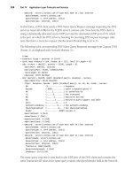
A test circuit was designed to allocate signal changes based on the weights
assigned during simulation. This hardware scheme is illustrated in Figure 9.10. An
LFSR generates n-bit patterns. These patterns drive a 1 of 2
n
selector or decoder. A
subset j
k
of the outputs from the selector drive bit-changer k which in turn drives
input k of the IC, where , and m is the number of inputs to the IC. The
number j
k
is proportional to the weight assigned to input k. The bit-changers are
designed so that only one of them changes in response to a change on the selector
outputs; hence only one primary input changes at the IC on any vector. When gener-
ating weights for the inputs, special consideration is given to reset and clock inputs
to the circuit.
Figure 9.10 Weighted pattern generator.
(a) (b)
j
k
k 1=
m
∑
2
n
≤
n
L
F
S
R
S
e
l
e
c
t
o
r
Bit
changer
Bit
changer
Bit
changer
Input 1
Input 2
Input m
468
BUILT-IN SELF-TEST
The WRP is also useful for combinational circuits where BIST is employed. Con-
sider, for example, a circuit made up of a single 12-input AND gate. It has 4096 pos-
sible input combinations. Of these, only one, the all-1s combination, will detect a
stuck-at-0 at the output. To detect a stuck-at-1 on any input requires a 0 on that input
and 1s on all of the remaining 11 inputs. If this circuit were being tested with an
LFSR, it would take, on average, 2048 patterns before the all-1s combination would
appear, enabling detection of a stuck-at-0 at the output. In general, this circuit needs
a high percentage of 1s on its inputs in order to detect any of the faults. The OR gate
is even more troublesome since an all-0s pattern is needed to test for a stuck-at-1
fault on the output, and the LFSR normally does not generate the all-0s pattern.
To employ WRPs on a combinational circuit, it is first necessary to determine
how to bias each circuit input to a 1 or a 0. The calculation of WRP values is based
on increasing the probability of occurrence of the nonblocking or noncontrolling
value (NCV) at the inputs to a gate.
14
For the AND gate mentioned previously, it is
desirable to increase the probability of applying 1s to each of its inputs. For an OR
gate, the objective is to increase the probability of applying 0s to its inputs. The
weighting algorithm must also improve the probability of propagating error signals
through the gate.
The first step in computing biasing values is to determine the number of device
inputs (NDI) controlling each gate in the circuit. This is the number of primary
inputs and flip-flops contained in the cone of that gate. This value, denoted as NDI
g
,
is divided by NDI
i
, the NDI for each input to that gate. That gives the ratio R
i
of the
NCV to the controlling value for each gate. This is illustrated in Figure 9.11, where
the total number of inputs to gate D, NDI
D
, is 9. NDI
A
is 4; hence the ratio R
i
of
NDI
D
to NDI
A
is 9 to 4. Two additional numbers, W0 and W1, the 0 weight and the
1 weight, must be computed for each gate in the circuit. Initially, these two values
are set to 1.
The algorithm for computing the weights at the inputs to the circuit proceeds as
follows:
1. Determine the NDI
g
for all logic gates in the circuit.
2. Assign numbers W0 and W1 to each gate; initially assign them both to 1.
Figure 9.11 Calculating bias numbers.
9:2
9:4
9:3
A
B
C
D
I
9
I
2
I
2
I
1
I
8
I
7
I
6
I
5
I
4
PO
RANDOM PATTERN EFFECTIVENESS
469
3. Backtrace from each output. When backtracing from a gate g to an input gate
i, adjust the weights W0 and W1 of gate i according to Table 9.1. When a gate
occurs in two or more cones, the value of W0 or W1 is the larger of the exist-
ing value and the newly calculated value.
4. Determine the weighted value WV. It represents the logic value to which the
input is to be biased. If W0 > W1, then WV = 0, else WV = 1.
5. Determine the weighting factor WF. It represents the amount of biasing toward
the weighted value. If WV = 0, then WF = W0/W1, else WF = W1/W0.
Example Consider the circuit in Figure 9.11. Initially, all the gates are assigned
weights W0 = W1 = 1. Then the backtrace begins. Table 9.2 tabulates the results.
When backtracing from gate D to gate A, Table 9.1 states that if gate g is an OR gate,
then W0
i
= (R
i
⋅ W0
g
) and W1
i
= W1
g
for gate i. In this example, gate g is the OR gate
labeled D and W0
g
= W1
g
= 1. Also, R
i
= 9/4. Thus, W0
i
= 9/4, or 2.25. In the next
step of the backtrace, g refers to gate A, an AND gate, and i refers to primary inputs
I
1
to I
4
. Also, R
i
= 4/1 = 4. The entry for the AND gate in Table 9.1 states that
W0
i
= W0
g
and W1
i
= (R
i
⋅ WI
g
). So the weights for I
1
to I
4
are W0
i
= 2.25 and
W1
i
= 4. The remaining calculations are carried out in similar fashion.
From the results it is seen that inputs I
1
to I
4
must be biased to a 1 with a weighting
factor WF = 4/2.25 = 1.77. Inputs I
5
and I
6
are biased to a 0 with WF = 4.5/2 = 2.25.
Finally, inputs I
7
to I
9
have identical 0 and 1 weights, so biasing is not required for
those inputs.
TABLE 9.1 Weighting Formulas
Logic Function
W0
i
W1
i
AND W0
g
R
i
.W1
g
NAND W1
g
R
i
.W0
g
OR R
i
.W0
g
W1
g
NOR R
i
.W1
g
W0
g
TABLE 9.2 Tabulating Weights
From (g) To (i)
W0
i
W1
i
PO gate D 11
gate D gate A 2.25 1
gate A
I
1
−I
4
2.25 4
gate D gate B 4.5 1
gate B
I
5
−I
6
4.5 2
gate D gate C 31
gate C
I
7
−I
9
33
470
BUILT-IN SELF-TEST
The calculation of weights for a circuit of any significant size will invariably lead
to fractions that are not realistic to implement. The weights should, therefore, be
used as guidelines. For example, if a weight is calculated to be 3.823, it is sufficient
to use an integer weighting factor of 4. The weighted inputs can be generated by
selecting multiple bits from the LFSR and performing logic operations on them. An
LFSR corresponding to a primitive polynomial will generate, for all practical pur-
poses, an equal number of 1s and 0s (the all-0s combination is not generated). So, if
a ratio 3:1 of 1s to 0s is desired, then an OR gate can be used to OR together two bits
of the LFSR with the expectation that, on average, one out of every four vectors will
have 0s in both positions. Similarly, for a ratio 3:1 of 0s to 1s the output of the OR
can be inverted, or an AND gate can be used. ANDing/ORing three or four LFSR
bits results in ratios of 7:1 and 15:1. More complex logic operations on the LFSR
bits can provide other ratios.
When backtracing from two or more outputs, there is a possibility that an input
may have to be biased so as to favor a logic 0 when backtracing from one output and
it may be required to favor a logic 1 when backtracing from another output. How
this situation is handled will ultimately depend on the method of test. If test patterns
are being applied by a tester that is capable of biasing pseudo-random patterns, then
it might be reasonable to use one set of weights for part of the test, then switch to an
alternate set of weights. However, if the test environment is complete BIST, a com-
promise might require taking some average of the weights calculated during the
backtraces. Another possible approach is to consider the number of inputs in each
cone, giving preference to the cone with a larger number of inputs since the smaller
cone may have a larger percentage of its complete set of input patterns applied.
Previously it had been mentioned that one approach to determining the weights
on the inputs could be accomplished by switching individual inputs one at a time
and measuring the internal activity in the circuit using a logic simulator. Another
approach that has been proposed involves using ATPG and a fault simulator to ini-
tially achieve high-fault coverage.
15
Use these test vectors to determine the fre-
quency of occurrence of 1s and 0s on the inputs. The frequency of occurrence helps
to determine the weighting factors for the individual circuit inputs. It would seem
odd to take this approach since one of the reasons for adopting BIST is to avoid the
use of ATPG and fault simulation, but the approach does reduce or eliminate the reli-
ance on a potentially expensive tester.
9.4.4 Aliasing
Up to this point the discussion has centered around how to improve fault coverage of
BIST while minimizing the number of applied vectors. An intrinsic problem that has
received considerable attention is a condition referred to as aliasing. If a fault is sen-
sitized by applied stimuli, with the result that an error signal reaches an LFSR or
MISR, the resulting signature generated by the error signal will map into one of 2
n
possible signatures, where n is the number of stages in the LFSR or MISR. It is pos-
sible for the error signature to map into the same signature as the fault-free device.
With 2
16
signatures, the probability that the error signal generated by the fault will
SELF-TEST APPLICATIONS
471
be masked by aliasing is 1 out of 2
16
, or about 0.0015%. If a functional register is
being used to generate signatures and if it has a small number of stages, thus intro-
ducing an unacceptably high aliasing error, the functional register can be extended
by adding additional stages that are used strictly for the purpose of generating a sig-
nature with more bit positions, in order to reduce the aliasing error.
9.4.5 Some BIST Results
The object of BIST is to apply sufficient patterns to obtain acceptable fault coverage,
recognizing that a complete exhaustive test is impractical, and that there will be
faults that escape detection. The data in Table 9.3 shows the improvement in fault
simulation, as the number of random test vectors applied to two circuits increases
from 100 to 10,000.
16
For the sake of comparison, fault coverage obtained with an ATPG is also listed.
The numbers of test patterns generated by the ATPG are not given, but another
ATPG under similar conditions (i.e., combinational logic tested via scan path)
generated 61 to 198 test vectors and obtained fault coverage ranging between 99.1%
and 100% when applied to circuit partitions with gate counts ranging from 2900 to
9400 gates.
17
9.5 SELF-TEST APPLICATIONS
This section contains examples illustrating some of the ways in which LFSRs have
been used to advantage in self-test applications. The nature of the LFSR is such
that it lends itself to many different configurations and can be applied to many
diverse applications. Here we will see applications ranging from large circuits with
a total commitment to BIST, to a small, 8-bit microprocessor that uses an ad hoc
form of BIST.
9.5.1 Microprocessor-Based Signature Analysis
It must be pointed out here that BIST, using random patterns, is subject to con-
straints imposed by the design environment. For example, when testing off-the-shelf
products such as microprocessors, characterized by a great deal of complex control
logic, internal operations can be difficult to control if no mechanism is provided for
that purpose. Once set in operation by an op-code, the logic may run for many clock
TABLE 9.3 Fault Coverage with Random Patterns
Number of
Gates
No. Random Patterns
Fault percentage
with ATPG
100 1000 10,000
Chip1 926 86.1 94.1 96.3 96.6
Chip2 1103 75.2 92.3 95.9 97.1
472
BUILT-IN SELF-TEST
cycles independent of external stimuli. Nevertheless, as illustrated in this section, it
is possible to use BIST effectively to test and diagnose defects in systems using off-
the-shelf components.
Hewlett-Packard used signature analysis to test microprocessor-based boards.
18
The test stimuli consisted of both exhaustive functional patterns and specific, fault-
oriented test patterns. With either type of pattern, output responses are compressed
into four-digit hexadecimal signatures. The signature generator compacts the
response data generated during testing of the system.
The basic configuration is illustrated in Figure 9.12. It is a rather typical micro-
processor configuration; a number of devices are joined together by address and data
buses and controlled by the microprocessor. Included are two items not usually seen
on such diagrams: a free-run control and a bus jumper. When in the test mode, the
bus jumper isolates the microprocessor from all other devices on the bus. In
response to a test signal or system reset, the free-run control forces an instruction
such as an NOP (no operation) onto the microprocessor data input. This instruction
performs no operation, it simply causes the program counter to increment through
its address range.
Since no other instruction can reach the microprocessor inputs while the bus
jumper is removed, it will continue to increment the program counter at each clock
cycle and put the incremented address onto the address bus. The microprocessor
might generate 64K addresses or more, depending on the number of address bits. To
evaluate each bit in a stream of 64K bits, for each of 16 address lines, requires stor-
ing a million bits of data and comparing these individually with the response at the
microprocessor address output. To avoid this data storage problem, each bit stream
is compressed into a 16-bit signature. For 16 address lines, a total of 256 data bits
must be stored.
The Hewlett-Packard implementation used the LFSR illustrated in Figure 9.2.
Because testability features are designed into the product, the tests can be run at the
product’s native clock speed, while the LFSR monitors the data bus and accumulates
a signature.
After the program counter has been verified, the ROM can be tested by running
through its entire address space and generating a signature on each of its output pins.
Figure 9.12 Microprocessor-based signature analysis.
Microprocessor
Bus jumper
Free
run
control
ROM
RAM
Peripherals
Control
Data bus
Address bus
SELF-TEST APPLICATIONS
473
The ROM, like the program counter, is run through its address space by putting the
board in the free run mode and generating the NOP instruction. After the ROM has
been checked, the bus jumper is replaced and a diagnostic program in ROM can be
run to exercise the microprocessor and other remaining circuits on the board. Note
that diagnostic tests can reside in the ROM that contains the operating system and
other functional code, or that ROM can be removed and replaced by another ROM
that contains only test sequences. When the microprocessor is in control, it can exer-
cise the RAM using any of a number of standard memory tests. Test stimuli for the
peripherals are device-specific and could in fact be developed using a pseudo-
random generator.
The signature analyzer used to create signatures has several inputs, including
START, STOP, CLOCK, and DATA. The DATA input is connected to a signal point
that is to be monitored in the logic board being tested. The START and STOP sig-
nals define a window in time during which DATA input is to be sampled while the
CLOCK determines when the sampling process occurs. All three of these signals are
derived from the board under test and can be set to trigger on either the rising or fall-
ing edge of the signal. The START signal may come from a system reset signal or it
may be obtained by decoding some combination on the address lines, or a special bit
in the instruction ROM can be dedicated to providing the signal. The STOP signal
that terminates the sampling process is likewise derived from a signal in the logic
circuit being tested. The CLOCK is usually obtained from the system clock of the
board being tested.
For a signature to be useful, it is necessary to know what signature is expected.
Therefore, documentation must be provided listing the signatures expected at the IC
pins being probed. The documentation may be a diagram of the circuit with the sig-
natures imprinted adjacent to the circuit nodes, much like the oscilloscope wave-
forms found on television schematics, or it can be presented in tabular form, where
the table contains a list of ICs and pin numbers with the signature expected at each
signal pin for which a meaningful signature exists. This is illustrated for a hypothet-
ical circuit in Table 9.4.
TABLE 9.4 Signature Table
IC Pin Signature IC Pin Signature
U21 2 8UP3 U41 3 37A3
3 713A 5 84U4
4 01F6 6 F0P1
7 69CH 8 1147
9 8P7U
9 77H1 11 684C
11 10UP 15 H1C3
14 1359
15 U11A
474
BUILT-IN SELF-TEST
During test the DATA probe of the signature analyzer is moved from node to
node. At each node the test is rerun in its entirety and the signature registered by the
signature analyzer is checked against the value listed in the table. This operation is
analogous to the guided probe used on automatic test equipment (cf. Section 6.9.3).
It traces through a circuit until a device is found that generates an incorrect output
signature but which is driven by devices that all produce correct signatures on their
outputs. Note that the letters comprising the signature are not the expected 0–9 and
A–F. The numerical digits are retained but the letters A–F have been replaced by
ACFHPU, in that order, for purposes of readability and compatibility with seven-
segment displays.
19
A motive for inserting stimulus generation within the circuits to be tested, and
compaction of the output response, is to make field repair of logic boards possible.
This in turn can help to reduce investment in inventory of logic boards. It has been
estimated that a manufacturer of logic boards may have up to 5% of its assets tied up
in replacement board kits and “floaters”—that is, boards in transit between customer
sites and a repair depot. Worse still, repair centers report no problems found in up to
50% of some types of returned boards.
20
A good test, one that can be applied suc-
cessfully to help diagnose and repair logic boards in the field, even if only part of the
time, can significantly reduce inventory and minimize the drain on a company’s
resources.
The use of signature analysis does not obviate the need for sound design prac-
tices. Signature analysis is useful only if the bit streams at various nodes are repeat-
able. If even a single bit is susceptible to races, hazards, uninitialized flip-flops, or
disturbances from asynchronous inputs such as interrupts, then false signatures will
occur with the result that confidence in the signature diminishes or, worse still, cor-
rectly operating components are replaced. Needlessly replacing nonfaulted devices
in a microprocessor environment can negate the advantages provided by signature
analysis.
9.5.2 Self-Test Using MISR/Parallel SRSG (STUMPS)
STUMPS was the outcome of a research effort conducted at IBM Corp. in the early
1980s for the purpose of developing a methodology to test multichip logic mod-
ules.
21
The multichip logic module (MLM) is a carrier that holds many chips. The
SRSG (shift register sequence generator) is their terminology for what is referred to
here as a PRG.
Development of STUMPS was preceded by a study of several configurations to
identify their advantages and disadvantages. The configuration depicted in
Figure 9.13, referred to as a random test socket (RTS), was one of those studied. The
PRG generates stimuli that are scanned into the MLM at the SRI (shift register
input) pin. The bits are scanned out at the SRO (shift register output) and are clocked
into a TRC to generate a signature. The scan elements are made up of LSSD SRLs
(shift register latches). Primary inputs are also stimulated by a PRG, and primary
outputs are sampled by a MISR. This activity is under control of a test controller that
determines how many clock cycles are needed to load the internal scan chains. The
SELF-TEST APPLICATIONS
475
Figure 9.13 Random test socket.
test controller also controls the multichip clocks (MCs). When the test is done, the
test controller compares the signatures in the MISR’s to the expected signatures to
determine if the correct response was obtained.
One drawback to the random test socket is the duration of the test. The assump-
tions are:
All of the SRLs are connected into a single scan path.
There would be about 10,000 SRLs in a typical scan chain.
The clock period is 50 ns.
About one million random vectors would be applied.
A new vector is loaded while the previous response is clocked into the MISR.
With these assumptions, the test time for an MLM is about 8 minutes, which was
deemed excessive.
A second configuration, called simultaneous self-test (SST), converts every SRL
into a self-test SRL, as shown in Figure 9.14(a). At each clock, data from the combi-
national logic is XOR’ed with data from a previous scan element, as shown in
Figure 9.14(b). This was determined to produce reasonably random stimuli. Since
every clock resulted in a new test, the application of test stimuli could be accom-
plished very quickly. The drawbacks to this approach were the requirement for a test
mode I/O pin and the need for a special device, such as a test socket, to handle test-
ing of the primary inputs and outputs.
A third configuration that was analyzed was STUMPS. The scan path in each
chip is driven by an output of the PRG (recall from the discussion of LFSRs that a
pseudo-random bit stream can be obtained from each SRL in the LFSR). The scan-
out pin of each chip drives an input to the MISR. This is illustrated in Figure 9.15,
where each chain from PRG to MISR corresponds to a one chip. The number of
clocks applied to the circuit is determined by the longest scan length. The chips with
shorter scan lengths will have extra bits clocked through them, but there is no pen-
alty for that. The logic from the primary outputs of each chip drive the primary
inputs to other chips on the MLM. Only the primary inputs and outputs of the MLM
have to be dealt with individually from the rest of the test configuration.
Multichip logic module
PRG
M
ISR
PRG TRC
Test
controller
PO’sPI’s
}
A
B
SRI
SRO
}
MCs
476
BUILT-IN SELF-TEST
Figure 9.14 Simultaneous self-test.
Unlike RTS, which connects the scan paths of all the individual chips into one
long scan path, scan paths for individual chips in STUMPS are directly connected to
the PRG and the MISR, using the LSSD scan-in and scan-out pins, so loading stim-
uli and unloading response can be accomplished more quickly, although not as
quickly as with SST. An advantage of STUMPS is the fact that, apart from the PRG
and MISR, it is essentially an LSSD configuration. Since a commitment to LSSD
has already been made and since STUMPS does not require any I/O pins in addition
to those committed to LSSD, there is no additional I/O penalty for the use of
STUMPS.
The PRG and MISR employed in STUMPS are contained in a separate test chip,
and each MLM contains one or more test chips to control the test process. A MLM
that contained 100 chips would require two test chips. Since the test chips are about
the same size as the functional chips, they represented about a 2% overhead for
STUMPS. The circuit in Figure 9.16 illustrates how the test chip generates the
pseudo-random sequences and the signatures.
Figure 9.15 STUMPS architecture.
Data
C
Scan-in
Shift A
Shift B
L1
L2
Test Mode
SRL
+
SRL
Data
Scan-in
Scan-out
Scan-out
(a)
(b)
+
+
Scan-in
MISR
PRG
SI
1
SI
2
SI
3
SI
n
SO
1
SO
2
SO
3
SO
N
Comb.
logic
Comb.
logic
SELF-TEST APPLICATIONS
477
Figure 9.16 The MISR/PRG chip.
9.5.3 STUMPS in the ES/9000 System
STUMPS was used by IBM to test the ES/9000 mainframe.
22
A major advantage in
the use of STUMPS was the ability to avoid creating the large test data files that
would be needed if ATPG generated vectors and response were used to test the ther-
mal conduction modules (TCM). A second advantage was simplification of TCM
cooling during testing due to the absence of a probing requirement.
A typical STUMPS controller chip contained 64 channels. The fault coverage
and the signatures generated by the circuits being tested were determined by simu-
lation. Tests applied included a flush test, a scan test, an ABT test, and a logic test.
The flush test (cf. Section 8.4.3) applies a logic 1 to both A and B clocks, causing
all latches to be opened from the scan-in to the scan-out. Then a 1, followed by a 0,
are applied to the scan chain input. This will reveal any gross errors in the scan
chain that prevents propagation of signals to the scan output. The scan test clocks
signals through the scan chain. The test is designed to apply all possible transitions
at each latch.
In an ABT test the module is switched to self-test mode and the LFSR and MISR
are loaded with initial values. Then all SRLs in the scan chains are loaded with
known values while the MISR inputs are blocked. After the SRLs are loaded, the
data are scanned into the MISRs. If the correct signature is found in the MISR, the
STUMPS configuration is assumed to be working correctly. A correct signature pro-
vides confidence that the self-test configuration is working properly.
After the aforementioned three tests are applied and there is a high degree of con-
fidence that the test circuits are working properly, the logic test mode is entered.
STUMPS applies stimuli to the combinational logic on the module and creates a sig-
nature at the MISR. The tests are under control of a tester when testing individual
modules. The tester applies stimuli to the primary inputs and generates signatures at
the primary outputs. The input stimuli are generated by LFSRs in the tester, which
SRL SRL
SO
i
SO
i+1
SRL SRL
0 1
MUX
0 1
MUX
TestMode
SI
i+1
SI
i+2
MISR
PRG
+
+
+
+
478
BUILT-IN SELF-TEST
are shifted once per test. Response at primary outputs is captured by means of SISRs
(single input signature registers) in the tester.
From the perspective of the engineers designing the individual chips, STUMPS
did not require any change in their methodology beyond those changes required to
accommodate LSSD. However, it did require changes to the Engineering Design
System (EDS) used to generate test stimuli and compute response.
23
A compiled
logic simulator was used to determine test coverage from the pseudo-random pat-
terns. However, before simulation commences, design rule checking must be per-
formed to ensure that X states do not find their way into the SRLs. If that happens,
the entire MISR quickly becomes corrupted. Predictable and repeatable signatures
was also a high priority.
For this particular development effort, the amount of CPU time required to gener-
ate a complete data file could range from 12 up to 59 hours. The data file for the
TCM that required 59 hours to generate contained 152 megabytes and included test
commands, signatures, and a logic model of the part. Fault coverage for the TCMs
ranged from 94.5% up to 96.5%. The test application time ranged from 1.3 minutes
to 6.2 minutes, with an average test time being 2.1 minutes.
Diagnosis was also incorporated into the test strategy. When an incorrect signa-
ture was obtained at the MISR, the test was repeated. However, when repeated, all
chains but one would be blocked. Then the test would be rerun and the signature for
each individual scan chain would be generated and compared to an expected signa-
ture for that chain. When the error had been isolated to one or more channels, the
test would be repeated for the failing channels. However, this time it was done in
bursts of 256 patterns in order to localize the failure to within 256 vectors of where it
occured. RAM writes were inhibited during this process so the diagnostic process
was essentially a combinational process. Further resolution down to eight patterns
was performed, and then offline analysis was performed to further resolve the cause
of the error signals. The PPSFP algorithm (Section 3.6.3) was used to support this
process, simulating 256 patterns at a time.
The test time for a fault-free module was, on average, 2.1 minutes. Data collec-
tion on a faulty module extended the test time to 5 minutes. Diagnostic analysis,
which included simulation time, averaged 11.7 minutes. Over 94% of faulty mod-
ules were repaired on the basis of automatic repair calls. Less than 6% of fails
required manual analysis, and the resolution of the diagnostics averaged less than
1.5 chips per defect. This resulted, in part, from fault equivalence classes than
spanned more than one chip.
9.5.4 STUMPS in the S/390 Microprocessor
Another product in IBM that made use of STUMPS was the S/390 microprocessor.
1
The S/390 is a single chip CMOS design. It incorporates pipelining and many other
design features found in contemporary high-end microprocessors. In addition, it
contains duplicate instruction and execution units that perform identical operations
each cycle. Results from the two units are compared in order to achieve high data
integrity. The S/390 includes many test features similar to those used in the ES/9000
SELF-TEST APPLICATIONS
479
system; hence in some respects its test strategy is an evolution of that used in the
ES/9000. A major difference in approaches stems from the fact that ES/9000 was a
bipolar design, with many chips on an MLM, whereas S/390 is a single-chip micro-
processor, so diagnosing faulty chips was not an issue for S/390.
The number of tester channels needed to access the chip was reduced by
placing a scannable memory element at each I/O, thus enabling I/Os to be
controlled and observed by means of scan operations. Access to this boundary
scan chain, as well as to most of the DFT and BIST circuitry, was achieved by
means of a five wire interface similar to that used in the IEEE 1149.1 standard
(cf. Section 8.6.2). An on-chip phase-locked loop (PLL) was used to multiply the
tester frequency, so the tester could be run at a much slower clock speed. Because
much of the logic dedicated to manufacturing test on the chips was also used for
system initialization, recovery, and system failure analysis, it was estimated that
the logic used exclusively for manufacturing test amounted to less than 1% of the
overall chip area.
One of the motivating factors in the choice of BIST was the calculation that the
cost of each full-speed tester used to test the S/390 could exceed $8 million. The
choice of STUMPS permitted the use of a low-cost tester by reducing the complex-
ity of interfacing to the tester. In addition, use of the PLL made it possible to use a
much slower, hence less expensive, tester. BIST for memory test eliminated the need
for special tester features to test the embedded memory. Another attraction of BIST
is its applicability to system and field testing.
Because the S/390 is a single, self-contained chip, it was necessary to design test
control logic to coexist on the chip with the functional logic. Control of the test
functions is accomplished via a state machine within each chip, referred to as the
self-test control macro (STCM). When in test mode, it controls the internal test
mode signals as well as the test and system clocks. Facilities exist within the STCM
that permit it to initiate an entire self-test sequence via modem. In addition to the
BIST that tests the random combinational logic, known as LBIST (logic BIST),
another BIST function is performed by ABIST (array BIST), which provides at-
speed testing of the embedded arrays. An ABIST controller can be shared among
several arrays. This both reduces the test overhead per array and permits reduced test
times, since arrays can be tested in parallel. The STUMPS logic tests are supple-
mented by weighted random patterns (WRP) that are applied by the tester. Special
tester hardware causes individual bits in scan-based random test patterns to be statis-
tically weighted toward 1 or 0.
The incorporation of BIST in the S/390 not only proved useful for manufacturing
and system test, but also for first silicon debug. One of the problems that was
debugged using BIST was a noise problem that would allow LBIST to pass in a nar-
row voltage range. Outside that range the signatures were intermittent and nonre-
peating, and they varied with voltage. A binary search was performed on the LBIST
patterns using the pattern counter while running in the good voltage range. The good
signatures would be captured and saved for comparison with the signatures gener-
ated outside the good voltage range. This was much quicker than resimulating, and it
led to the discovery of the noisy patterns that had narrow good response voltage
480
BUILT-IN SELF-TEST
windows. These could then be applied deterministically to narrow down the source
of the noise.
LBIST was also able to help determine power supply noise problems. LBIST
could be programmed to apply skewed or nonskewed load/unload sequences with or
without system clocks. The feature was used to measure power supply noise at dif-
ferent levels of switching activity. LBIST was able to run in a continuous loop, so it
was relatively easy to trace voltage and determine noise and power supply droop
with different levels of switching activity. Some of these same features of LBIST
were useful in isolating worst-case delay paths between scan chains.
9.5.5 The Macrolan Chip
The Macrolan (medium access controller) chip, a semicustom circuit, was designed
for the Macrolan fiber-optic local area network. It consists of about 35,000 transis-
tors, and it used BIST for its test strategy.
2
A cell library was provided as part of the
design methodology, and the cells were able to be parameterized. A key part of the
test strategy was a register paracell, which could be generated in a range of bit sizes.
The register is about 50% larger than a scan flip-flop, and each bit contained two
latches, permitting master/slave, edge-triggered, or two-phase, nonoverlapping
clocking. All register elements are of this type, there are no free-standing latches or
flip-flops. Two diagnostic control bits (DiC) from a diagnostic control unit permitted
registers to be configured in four different modes:
User—the normal functional mode of the register
Diagnostic hold—contents of the register are fixed
Diagnostic shift—data are shifted serially
Test
LFSR
MISR
Generate circular shifting patterns
Hold a fixed pattern
When in test mode, selection of a particular test function is accomplished by
means of two bits in the test register. These two bits, as well as initial seed values
for generating tests, are scanned into the test register. Since the two control bits
are scanned in, the test mode for each register in the chip can be individually
selected. Thus, an individual scan chain can be serially shifted while others are
held fixed.
The diagnostic control unit is illustrated in Figure 9.17. In addition to the clock
(CLK), there are four input control signals and one output signal. Three other sig-
nals are available to handle error signals when the chip is used functionally. The chip
select (CS) makes it possible to access a single chip within a system. Control (CON)
is used to differentiate between commands and data. Transfer (TR) indicates that
valid data are available and Loop-in is used to serially shift in commands or data.
Loop-out is a single output signal.
SELF-TEST APPLICATIONS
481
Figure 9.17 Macrolan diagnostic unit.
The diagnostic unit can control a system of up to 31 scan paths, each containing
up to 128 bits. As previously mentioned, scan paths can be individually controlled
using the two DiC bits. Scan path 0 is a 20-bit counter that is serially loaded by the
diagnostic unit. It determines the number of clock cycles used for self-test; hence the
system can apply a maximum of 2
20
patterns. This limitation of 20 bits is imposed to
minimize the simulation time required to compute signatures as well as to limit test
time. The diagnostic unit can support chips using two or more clocks, but all regis-
ters must be driven from a master clock when testing the chip or accessing the scan
paths.
The Macrolan chip makes use of a fence multiplexer to assist in the partitioning
of the circuit. This circuit, illustrated in Figure 9.18, is controlled by a register
external bit. During normal operation the register external bit is programmed to
select input A, causing the fence to be logically transparent. When testing the chip,
the fence plays a dual role. If input A is selected, the input to the fence can be
compacted using the LFSR/MISR. When the external bit selects input B, the fence
can be used in the generation of random patterns to test the logic being driven by
the fence. Fences are also used to connect I/O pins to internal logic. This permits
chips to be isolated from other circuitry and tested individually when mounted on
a PCB.
Since the counter limits the number of tests to 2
20
, a cone of combinational logic
feeding an output cannot be tested exhaustively if it has more than 20 inputs. Since
each output in a scan chain must satisfy that criteria with respect to the inputs to the
Function / data
Function decode
and control
Loop
number
Command
5:32
decode
DC1 select
Detect Control
Counter (LPO)
Loop 1
Loop 2
Loop N
32:1
MUX
Loop
out
Loop in
DC2
TR
CS
CON
CLK
482
BUILT-IN SELF-TEST
Figure 9.18 Fence multiplexer.
cone, and since logic cones, in general, are going to share inputs, a true exhaustive
test for all the logic is virtually impossible to achieve. It is estimated that about 5%
of the logic on the Macrolan chip is tested using exhaustive testing.
The BIST strategy employed by the design team made use of quasiexhaustive
test. This test mode takes advantage of the observation that if 1 < N < 17, where N is
the number of inputs to a circuit, and if there are M = 2
N+3
random vectors (i.e.,
without replacement), then P
M
≥ 99.9%. Therefore, the LFSR can be cycled through
a small subset of its patterns, with the result that there is no upper limit on the length
of the LFSR, as there would be for an exhaustive test.
Another advantage to this mode of test is that two LFSRs can be used to generate
patterns in parallel as long as their lengths are different. Consider two LFSRs of
length A and B that generate maximal length sequences S
A
= 2
A
− 1 and S
B
= 2
B
− 1.
The longest possible sequence generated by the two LFSRs running in parallel is
(2
A
− 1) × (2
B
− 1), in which case their combined sequence will not repeat until
both LFSRs return to their seed values simultaneously. The sequence length then
will be the lowest common multiple of S
A
and S
B
, that is, S
A+B
= S
A
× S
B
. Put
another way, the highest common factor (HCF) of S
A
and S
B
must be 1, which makes
the sequence lengths of A and B coprime.
9.5.6 Partial BIST
Up to this point BIST has been discussed within the context of an all-or-nothing
environment. But many test strategies employ BIST as one of several strategies to
achieve thorough, yet economical test coverage. In particular, it is not uncommon to
see designs where there is a sizable internal RAM that is tested using memory BIST
or ROM that is tested by generating a signature on its contents while the random
logic circuitry employs scan-based DFT. The PowerPC MPC750 is an example of a
design that uses memory BIST (memory BIST will be discussed in Chapter 10). The
MPC750 also employs functional patterns to test small arrays, clock modes, speed
sorting, and other areas that were not fully tested by scan.
24
The Pentium
Pro employed a BIST mode to achieve high toggle coverage for
burn-in testing.
25
However, this feature was not intended to achieve high-fault cover-
age. Some LFSRs were used to support BIST testing of programmable logic arrays
LFSR
MISR
Register
external bit
MUX
SEL
A
B
SELF-TEST APPLICATIONS
483
(PLAs). Interestingly, their cost/benefit analysis led them to implement equivalent
functionality in microcode for the larger PLAs. Signatures from the PLAs during
BIST were acquired and read out using a proprietary Scanout mode under micro-
code control. In an earlier Intel paper describing the use of BIST for PLAs and
microcode ROM (CROM), it was pointed out that the use of BIST during burn-in
made it possible to detect a high percentage of early life failures.
26
While there is growing interest in BIST, and it becomes easier to justify as cir-
cuits get larger and feature sizes get smaller, design teams have been able to justify it
on the basis of cost/benefit analysis as far back as the early 1980s. The Motorola
MC6804P2 is externally a small 8-bit microprocessor, but internally it is a serial
architecture. It used BIST because it was determined to be cost effective as a test
solution.
27
A 288-byte test program is stored in on-chip ROM; and an on-chip
LFSR, using the CCITT-16 polynomial x
15
+ x
12
+ x
5
+ 1, is updated at the end of
each clock during the execution of the test program. A verify mode uses the same
LFSR to test both customer and self-test ROM. The results are then compressed into
a single 16-bit signature. The LFSR monitors the data bus so that during execution
of the test program it is seldom necessary to perform compare and conditional
branch instructions.
A flowchart for the MC6804P2 self-test is illustrated in Figure 9.19. The first step
of the test checks basic ALU operations and writes results to a four-level stack. The
ports and interrupt logic are then tested. The ports can be driven by a tester for
worst-case test, or they can be tied together with a simple fixture for field test. After
the test, the LFSR is read out and the 32-byte dynamic RAM is tested, and results
are again read out. Then the RAM is filled with all-zeros, and those data are checked
at the end of the test to confirm data retention. Again, after the timer test, the results
are shifted out and a pass/fail determination is made. Finally, the data ROM test is
used to test the data space ROM, the RAM that was previously cleared, the accumu-
lator, and other miscellaneous logic.
The 288 bytes of test program are equivalent to about 1500 bus cycles. It was
estimated that because of the serial nature of the microprocessor, each bus cycle was
equivalent to about 24 clock cycles; hence the test would require about 36,000 test
vectors. The customer ROM would add another 9000 vectors. Another factor
impacting test size is the fact that the test program, if controlled by a tester, would
need more compares, data reads, and so on, to replace the reads performed by the
internal LFSR. Another motive for the BIST was its availability to customers.
Figure 9.19 Self-test flowchart.
STACK
PORTS
RAM
TIMER
DATA ROM
PASS
FAIL
484
BUILT-IN SELF-TEST
9.6 REMOTE TEST
Monitoring and testing electronic devices from a distant test station has been a fun-
damental capability for many years. However, it has tended to be quite expensive,
and hence reserved for those applications where its cost could be justified. In former
years it had been reserved for large, expensive mainframes and complex factory con-
trollers. This mode of operation has recently migrated to more common devices,
including the personal computer.
9.6.1 The Test Controller
In years gone by, the test controller was an indispensable part of the overall test
strategy in many applications, including large mainframes and complex electronics
systems for controlling avionics and factory operations, where a system might be
comprised of several units, each comprised of many hundreds of thousands of logic
gates. It might have different names and somewhat different assignments in different
systems, but one thing the test controllers had in common was the responsibility to
respond to error symptoms and help diagnose faults more quickly. Test controllers
used some or all of the methods discussed in this and previous chapters, and they
used some methods that will be discussed in subsequent sections. The general range
of functions performed by the test controller include the following:
System startup
Communications with operator
System reconfiguration
Performance monitoring
System testing
Some of the earliest test controllers were used in support of mainframes. The typ-
ical test controller was a minicomputer or microprocessor. The rationale for this
approach resulted from the fact that the mainframe was implemented using a tech-
nology such as emitter-coupled logic (ECL), which ran quite hot. As a result, it was
much less reliable than the minicomputer or microprocessor that was used to apply
test programs when the mainframe was powered up or when a problem occurred.
A typical system configuration is depicted in Figure 9.20. During system startup
the test controller, or maintenance processor as it was sometimes called, was
required to initialize the main processor, set or reset specific flip-flops and indica-
tors, clear I/O channels of spurious interrupt requests, load the operating system,
and set it into operation. Communication with the operator might result in operator
requests to either conduct testing of the system or make some alterations to the stan-
dard configuration. A system reconfiguration might also be performed in response to
detection of errors during operation. Detection of a faulty I/O channel, for example,
might result in that channel being removed from operation and I/O activities for that
channel being reassigned to another channel. Some or all of the reconfiguration was
performed in conjunction with the main processor.
REMOTE TEST
485
Figure 9.20 The maintenance processor.
Performance monitoring requires observing error indicators within a system dur-
ing operation and responding appropriately. It is not uncommon for a maintenance
processor to become aware of a problem before the computer operator realizes it. If
an error signal is observed, an instruction retry may be in order. If the retry results in
another error indication of the same nature, then a solid failure is indicated and a
detailed test of some part of the system is necessary. The maintenance processor
must determine what tests to select, and it must record the internal state of the sys-
tem so that it can be restarted, whenever possible, from the point where the error was
detected.
After applying tests, decisions must be made concerning the results of the tests.
This may involve communicating with a field engineer either locally or, via remote
link, at some distant repair depot. If tests do not result in location of a fault, but the
error persists, then the field engineer may want to load registers and flip-flops in the
system with specific test data via the maintenance processor, run through one or
more cycles of the system clock, and read out the results for evaluation.
In conjunction with remote diagnosis, it is possible to maintain a database at a
depot to assist the field engineer in those situations where the error persists but a
fault cannot be located. The Remote Terminal Access Information Network
(RETAIN) system is one such example.
28
It is a data base of fault symptoms that
proved difficult to diagnose. It includes the capability for structuring a search argu-
ment for a particular product symptom to provide efficient and rapid data location.
The data base is organized both on a product basis and on a symptom basis.
It should be noted that the maintenance processor must be verified to be working
correctly. However, the computer chosen to serve as the maintenance processor was
normally a mature product rather than a state-of-the-art device; it need not be fast,
only reliable. Hence, it was generally orders of magnitude more reliable than the
mainframe it was responsible for testing.
In microprogrammable systems implemented with writable control store, the
maintenance processor can be given control over loading of control store. This can
be preceded at system start-up time by first loading diagnostic software that operates
out of control store. Diagnostics written at this level generally exercise greater con-
trol over internal hardware. Tests can run more quickly since they can be designed to
Modem
Maintenance
computer
Test
interface
Mainframe
Remote
console
486
BUILT-IN SELF-TEST
exercise functional units without making repeated instruction fetches to main mem-
ory. In addition, control at this level makes it possible to incorporate hardware test
features such as BILBOs and similar BIST structures, and directly control them
from fields in the microcode.
Maintenance processors can be given control over a number of resources, includ-
ing power supplies and system clocks.
29
This permits power margining to stress
logic components, useful as an aid in uncovering intermittents. Intermittents can
also occasionally be isolated by shortening the clock period. With an increased sys-
tem clock period, the system can operate with printed circuit boards on extender
cards. Other reconfiguration capability includes the ability to disconnect cache and
address translation units to permit operation in a degraded mode if errors are
detected in those units.
The maintenance processor must be flexible enough to respond to a number of
different situations, which suggests that it should be programmable. However,
operating speed of the maintenance processor is usually not critical, hence micro-
processor-based maintenance processors were used. One such system reported in the
literature used a Z80 microprocessor.
30
The maintenance processor can trace the
flow of activity through a CPU, which proves helpful in writing and debugging both
diagnostic and functional routines in writable control store. Furthermore, the main-
tenance processor can reconfigure the system to operate in a degraded mode wherein
an IPU (internal processor unit) that normally shares processing with the CPU can
take over CPU duties if the CPU fails.
Another interesting feature of the maintenance processor is its ability to inten-
tionally inject fault symptoms into the main processor memory or data paths to
verify the operation of parity checkers and error detection and correction circuitry.
31
The logging of relevant data is an important aspect of the maintenance processor’s
tasks. Whenever indicators suggest the presence of an error during execution of an
instruction, an instruction retry is a normal first response since the error may have
been caused by an intermittent condition that may not occur during instruction retry.
Before an instruction retry, all data that can help to characterize the error must be
captured and stored. This includes contents of registers and/or flip-flops in the unit
that produced the error signal. Other parameters that may be relevant include tem-
perature, line voltage, time, and date.
32
If intermittents become too frequent, it may
be possible to correlate environmental conditions with frequency of occurrence of
certain types of intermittent errors. If a given unit is prone to errors under certain
stressful conditions, and if this is true in a large number of units in use at customer
sites, the recorded history of the product may indicate an area where it may benefit
from redesign.
The inclusion of internal busses in the mainframe to make internal operations
visible is also supported.
33
An interesting addition to this architecture is the cyclic
redundancy check (CRC) instruction, which enables both the operational program-
mer and the diagnostic programmer to generate signatures on data buffers or instruc-
tion streams.
The scan path can be integrated with the maintenance processor, as in the
DPS88.
34
In this configuration the maintenance processor has access to test vectors
REMOTE TEST
487
stored on disk. The tests may be applied comprehensively at system start-up or may
be applied selectively in response to an error indication within some unit. The tests
are applied to specific scan paths selectable from the maintenance processor. The
scan path is first addressed and then the test vectors are scanned into the addressed
serial path. Addressability is down to specific functional unit, board, and micropack
(assembly on which 50 to 100 dice are mounted and soldered). The random pattern
and signature features can be used in conjunction with the maintenance processor.
16
9.6.2 The Desktop Management Interface
With the pace of technology permitting CMOS to overtake ECL technology, micro-
processors with a clock period of 1.0 ns and less at the time of this writing are replac-
ing mainframes of little more than a decade ago. The maintenance processor is not as
common as it once was. However, the now ubiquitous personal computer (PC) has
introduced a different set of problems. The mass production of millions of these PCs
puts complex devices that are difficult to test and diagnose when they fail to work
correctly into virtually every business and household. Furthermore, these PCs can be
difficult to set up or alter if the owner wants to perform an upgrade. Clashes over soft-
ware settings between application programs, or clashes over switch settings on the
motherboard, can lead to significant frustration on the part of the owner of the PC.
A solution to this situation is the Desktop Management Interface (DMI). This is a
specification defined by a consortium of vendors known as the Desktop Manage-
ment Task Force (DMTF).
35
DMI 2.0 includes a remote management solution that
makes it possible to access information across the internet by means of standard
Remote Procedure Calls (RPC). The goal is to address cost of ownership problems.
By developing standardized procedures for communicating between components of
a system, it becomes possible to identify and report everything from simple opera-
tional problems, such as a device out of paper, to software problems such as conflict-
ing interrupt settings, to hardware problems such as a CPU fan failure or an
imminent hard disk head crash.
The general organization of the DMI is illustrated in Figure 9.21. The service
layer collects information from the component interface, which in turn collects data
from the hardware and software components. One of the components is an ASIC
that collects data indicating excessive temperature, incorrect voltages, fan failures,
and chassis intrusions. Information collected by the component interface is stored in
a management information file (MIF) data base.
The management application gathers information from the MIF data base and the
service layer via the management interface and reports the data by means of a
graphical user interface (GUI). The management application can run on a remote
console or on the client. System files for particular managed components can be
updated when the product itself is being updated. Vendors of managed products pro-
vide the component interface—that is, test programs, data, and product attributes in
MIF format. DMI requires a compatible BIOS that can communicate with the com-
ponent interface and service provider. Some information, such as conflicting inter-
rupt assignments or low memory or disk space, comes from the operating system.
488
BUILT-IN SELF-TEST
Figure 9.21 Desktop Management Interface (DMI).
Some of the information for DMI comes from operational modes that report such
routine problems as paper jams, open cover, or low levels of toner or paper in a
printer. Other information comes from more sophisticated analysis tools such as the
hard drive reliability standard called Self-Monitoring, Analysis and Reporting Tech-
nology (SMART). This standard provides for on-drive sensing hardware for report-
ing drive status and software to collect and intrepret that data. The object is to
measure physical degradation in the drive and alert the user to imminent failures.
These measurements are recorded in the hard drive by sensor chips that potentially
can measure up to 200 parameters such as head flying height, spin-up time, and so
on. If a measurement falls outside of some predefined range, the drive issues an
alarm that can be directed to the DMI which can display the measurement on its
GUI.
36
9.7 BLACK-BOX TESTING
This chapter began with a look at circuits designed to generate stimuli and accumu-
late response patterns, or signatures. These basic tools were then used, in conjunc-
tion with maintenance processors and scan methodologies, to test large mainframes.
The solution was a global application of scan to all of the circuitry. We now turn our
attention to the testing of circuits where, for various reasons, there is no visibility
into the internal structure of the device or system. All testing is performed based on
an understanding of the functionality of the device. Because of this lack of visibility,
the methods described here are often referred to as black-box testing.
Testing of microprocessors and other complex logic devices can be aided by
ordering and/or partitioning the functions within these devices. Ordering offers
insight into the order in which functions should be tested. Furthermore, a good,
robust ordering may suggest test strategies, since different partitions may lend
Service layer
Component interface
Management interface
Management
information
data base
Desktop
mgmt. appl.
Mgmt.
console
LAN mgmt.
application
Motherboard
Scanner
Monitor
Hard drive
Operating
system
Appl.
SW
Plotter
Management
Applications
Managed
Products
BLACK-BOX TESTING
489
themselves to very different test methodologies. Where one partition may best be
tested with BIST, another partition may be more effectively, or economically, tested
using a conventional ATPG. A successful ordering of partitions may also be critical
for those situations where detailed knowledge of the physical structure of the
system is not available. In such cases, algorithmic test programs, such as those dis-
cussed in Chapter 7 for ALUs, counters, and so on, may be necessary. Within that
context, it is necessary to develop a test program that is thorough while at the same
time effective at diagnosing fault locations.
9.7.1 The Ordering Relation
A typical central processor unit (CPU) is illustrated in Figure 9.22. The figure is also
typical of the amount of information provided by manufacturers of microprocessors.
The information is usually provided for the benefit of the assembly language pro-
grammer. It displays a register stack, a control section, an ALU, a status register, a
data bus, instruction register, and program counter. Information is provided on the
architecture, including the instruction set, and a breakdown of the number of
machine cycles required to execute the instructions.
Two or three decades ago, when the 8-bit microprocessor was dominant, it was
not unusual to create a gate equivalent circuit and run ATPG. For contemporary,
multi-million gate circuits, that is virtually impossible. An alternative is to resort to
the use of block diagrams. In the method to be described here, a system is first parti-
tioned into macroblocks, which are high-level functional entities such as CPUs,
memory systems, interrupt processors, I/O devices, and control sections.
37
The
macroblocks are then partitioned, to the extent possible, into smaller microblocks.
Testing is organized at the microblock level, hence can be quite detailed, and can take
into account the characteristics of the individual microcircuits. The objective is to
obtain a comprehensive test for the microblock while using the macroblocks to route
Figure 9.22 Typical central processor unit.
Data bus
MUX
Acc
Status
Program
counter
Inst. reg.
Main
memory
Control unit
ALU
Address bus
C
n
C
2
C
1
Regs.
490
BUILT-IN SELF-TEST
test information to observable outputs. When testing the microblocks in a given
macroblock, all other macroblocks are assumed to be fault-free. Furthermore, the
microblocks within a given macroblock are ordered such that a microblock is tested
only through modules already tested.
Before discussing partitioning techniques for microblocks and macroblocks, we
discuss the concept of hardcore. Hardcore circuits are those used to test a processor.
First-degree hardcore is circuitry used exclusively for testing. It is verified indepen-
dently of a processor’s normal operational features and is then used to test the oper-
ational logic. Examples of first-degree hardcore include such things as a ROM
dedicated to test which is loaded via a special access path not used by operational
logic, a dedicated comparator for evaluating results, and watchdog timers that are
used to verify that peripherals attached to the I/O ports respond within some speci-
fied time. A given device may or may not have first-degree hardcore. If it does, then
the test strategy dictates that it be tested first. Second-degree hardcore is that part of
the operational hardware used in conjunction with first-degree hardcore to perform
test functions. Examples of this include the writable control store (WCS) used by
test microprograms to exercise other operational units as well as the control circuitry
and access paths of the WCS.
After first-degree hardcore has been verified, the second-degree hardcore is veri-
fied. Then the macroblocks are selected for testing. These are chosen such that a
macroblock to be tested does not depend for its test on another macroblock that has
not yet been tested. Individual microblocks within a chosen macroblock are selected
for testing, again with the requirement that microblocks be tested only through
other, previously tested microblocks. To achieve this, two ordering relations are
defined. The controllability relation
ρ
1
is defined by
A ⋅
ρ
1
⋅ B ⇔ A can be controlled through B
The observability relation
ρ
2
is defined by
A ⋅
ρ
2
⋅ B ⇔ A can be observed through B
With these two relations, a priority partial order ≥ is defined such that
If B ⋅
ρ
1
⋅ a and B ⋅
ρ
2
⋅ b, then B ≥ a ⋅ b
In words, a test of B must follow the test of a AND b. In effect, if B is controlled
through a and observed through b, then a and b must both be tested before B is
tested. However, it may be that two devices C and D have the property that C ≥ D
and D ≥ C. In that case A ≡ B and A and B are said to be indistinguishable. This
would be the case, for example, if two devices were connected in series and could
not possibly be tested individually. After a complete ordering has been established,
the microblocks are partitioned into layers such that each microblock is tested only
BLACK-BOX TESTING
491
through microblocks contained in previous layers. A microblock B is contained in a
layer L
k
if and only if
1. B follows at least one element of L
k−1
2. All elements smaller than B are contained in the union .
Layer L
0
is the hardcore; it is directly controllable and observable.
To assist in ordering microblocks, a tree is formed as illustrated in Figure 9.23. In
that figure, the dot (⋅) represents the AND operator and the plus (+) represents the OR
operator. Therefore, B ≥ C ⋅ D + E ⋅ F states that the test of B must follow either the
test of C AND D, OR it must follow the test of E AND F. In this graph, if an element
occurs twice on the graph, with elements in between, then an indistinguishability
block is defined that contains all elements joining the two occurrences of the element.
Example The ordering algorithm will be illustrated by means of the circuit in
Figure 9.24. The various elements in that circuit are assigned numbers to identify
them during the discussion that follows. We first identify the
ρ
1
and
ρ
2
relations:
From these relations the following ordering relations can be derived:
1 ≥ 0
2 ≥ 4
3 ≥ 4 ⋅ 5
4 ≥ 1 ⋅ 2 + 1 ⋅ 3
5 ≥ 3 ⋅ 4
Figure 9.23 Ordering tree.
Controlled by Observed through
1
ρ
1
01
ρ
2
0
2
ρ
1
02
ρ
2
4
3
ρ
1
53
ρ
2
4
4
ρ
1
1 ⋅ (2 + 3) 4
ρ
2
0
5
ρ
1
45
ρ
2
3
L
i
i 0=
k 1–
∪
+
B
k
B
11
B
1n
B
12
B
j1
B
jn
B
j2