McGraw-Hill PDA Robotics 2003 (By.Laxxuss) Part 7 pptx
Bạn đang xem bản rút gọn của tài liệu. Xem và tải ngay bản đầy đủ của tài liệu tại đây (374.92 KB, 20 trang )
tery pack. The grounds are, and must be, connected (common ground).
The circuit’s block diagram is shown in Figure 5.42.
Maximum Ratings. The maximum ratings are shown in Figure 5.43.
I really like this chip because it will shut down if it is overloaded and
becomes hot. It is a nasty sight (and smell) seeing a smoke plume
when an overloaded component like a transistor melts down. The
L298 can handle a respectable load for its compact size (3 amps, 25
watts). It might be overkill for the motors it drives in this project, but
it also means that you can connect much more powerful motors if you
decide to change the design. The enable feature and the 2-pin logic
lines (with a wide voltage range of –0.3 to 7 V) per side makesa great
logic interface. ST microelectronics and Protel provide the footprint
and profile for use in the Protel 98 and Protel DXP circuit design pro-
grams allowing you to simply drop the chip into your circuit design.
Figure 5.44 a picture of the package we are using in the project show-
ing the pin layout. The short pins are set forward, and the longer are
to the back of the chip.
Table 5.5
Pin Descriptions
Pins Name Function
1,15 Sense A; Sense B Between this pin and ground is the sense resistor
connected to control the current of the load.
2,3 Out 1; Out 2 Outputs of the Bridge A; the current that flows through
the load connected between these two pins is monitored
at pin 1.
(continued on next page)
PDA Robotics
98
Figure 5.43
Maximum ratings.
PDA 05 5/30/03 11:35 AM Page 98
Table 5.5
Pin Descriptions (continued)
Pins Name Function
4 Vs Supply Voltage for the Power Output stages. A
noninductive 100nF capacitor must be connected
between this pin and ground.
5,7 Input 1; Input 2 TTL Compatible Inputs of the Bridge A.
6,11 Enable A; EnableB TTL Compatible Enable Input: the L state disables the
bridge A (enable A) and/or the bridge B (enable B).
8 GND Ground.
9 VSS Supply Voltage for the Logic Blocks. A100nF capacitor
must be connected between this pin and ground.
10,12 Input 3; Input 4 TTL Compatible Inputs of the Bridge B.
13,14 Out 3; Out 4 Outputs of the Bridge B. The current that flows through
the load connected between these two pins is monitored
at pin 15.
Figure 5.45 shows how to wire one side of the chip for bidirectional
motor control. This is how the chip is wired in PDA Robot. Pins 10
and 12 are connected to Port B pins on the PIC16F876 that have been
configured through the C code as outputs (see Chapter 7: Programming
the PIC16F876 Microcontroller). In PDA Robot, the sense pins 1 and
15 are tied to the ground. We can feed this into one of the analog pins
on the PIC16F876 and determine the current draw on the motors
(explained below). If the motor is drawing too much current, shut it
down. You can experiment with this. A command could be sent to the
Chapter 5 / The Electronics
99
Figure 5.44
L298 pin layout.
PDA 05 5/30/03 11:35 AM Page 99
PDA Robotics
100
Figure 5.46
Paralleled channels
for high current.
Figure 5.45
Bidirectional motor
control. (C = 1 and
D = 0 ) Forward, (C
= 0 and D = 1)
Reverse, (C = D)
Fast Motor Stop.
PDA 05 5/30/03 11:35 AM Page 100
robot to retrieve and forward this information to the PDA (like the
range-finder information), where it can be displayed and analyzed. We
could determine the speed of PDA Robot based on the current draw
after calibrating on a hard, flat surface. This is not a very accurate
method of determining the speed and distance traveled, but it will
give you a good estimate. Things like the incline and traction will
affect the accuracy.
For higher currents, outputs can be paralleled. Take care to parallel
channel 1 with channel 4 and channel 2 with channel 3. Figure 5.46
shows how to accomplish this.
Power Output Stage. The L298 integrates two power output stages
(A; B). The power output stage is a bridge configuration, and its out-
puts can drive an inductive load in common or differential mode,
depending on the state of the inputs. The current that flows through
the load comes out from the bridge at the sense output. An external
resistor (RSA; RSB) allows one to detect the intensity of this current.
Input Stage. Each bridge is driven by means of four gates, the input
of which are In1; In2; EnA and In3; In4; EnB. The In inputs set the
bridge state when the En input is high; a low state of the En input
inhibits the bridge. All the inputs are TTL compatible.
Suggestions. A noninductive capacitor, usually of 100 nF, must be
foreseen between both Vs and Vss to ground as near as possible to
GND pin. When the large capacitor of the power supply is too far from
the IC, a second smaller one must be near the L298. The sense resis-
tor, not of a wire wound type, must be grounded near the negative pole
of Vs that must be near the GND pin of the IC. Each input must be con-
nected to the source of the driving signals by means of a very short
path.
Turn on and turn off: Before you can turn on the supply voltage and
to turn it off; the enable input must be driven to the low state.
Applications. The external bridge of diodes D1 to D4 is made of four
fast recovery elements (trr 3 200 n) that must be chosen from a VF as
low as possible at the worst case of the load current. The sense output
voltage can be used to control the current amplitude by chopping the
Chapter 5 / The Electronics
101
PDA 05 5/30/03 11:35 AM Page 101
inputs, or to provide overcurrent protection by switching the enable
input to low.
The brake function (Fast motor stop) requires that the absolute maxi-
mum rating of 2 amps must never be overcome. When the repetitive
peak current needed from the load is higher than 2 Amps, a paralleled
configuration can be chosen.
An external bridge of diodes is required when inductive loads are
driven and when the inputs of the IC are chopped; Schottky diodes are
preferred. This solution can drive until 3 amps in DC operation and
until 3.5 amps of a repetitive peak current. The L298 is great for driv-
ing a stepper motor. Figure 5.47 shows how this is accomplished
when the current is controlled by a L6506.
The GP2D12 IR Range Finder
The GP2D12 is a low-cost, short-range IR alternative to ultrasonic
range-finding systems. Usable detection range is 10 cm to 80 cm
(approx. 4" to 31.5"). The IR Object Detection System consists of the
Sharp GP2D12 Distance Measuring Sensor. The GP2D12 is a compact,
PDA Robotics
102
Figure 5.47
Two phase bipolar stepper motor control circuit by using the current controller L6506.
PDA 05 5/30/03 11:35 AM Page 102
self-contained IR ranging system incorporating an IR transmitter,
receiver, optics, filter, detection, and amplification circuitry. The unit
is highly resistant to ambient light and nearly impervious to variations
in the surface reflectivity of the detected object.
Unlike many IR systems, it has a fairly narrow field of view, making it
easier to get the range of a specific target. The field of view changes
with the distance to an object, but is no wider than 5 cm (2.5 cm either
side of center) when measuring at the maximum range. One negative
about this range finder is its starting range of 10 cm. Figure 5.48 shows
the physical dimensions of the range finder and its connector
(www.hvwtech.com).
Chapter 5 / The Electronics
103
Figure 5.48
Physical dimensions of the range finder.
PDA 05 5/30/03 11:35 AM Page 103
The sensor unit may be mounted using the bracket provided. The
black foam should be applied to the bottom of the bracket using the
sticky side of the foam, and then the black “snap rivet” is pushed
through the large center hole on the bracket. This snap rivet has been
chosen to allow the bracket and foam to be mounted on a standard
0.062" PCB. A 13/64" hole is required in the PCB for the snap rivet.
Connecting to the Sensor
A custom cable assembly is included with the kit. The miniature con-
nector is keyed so that it may only be inserted one way: 1 Vcc Red ϩ
5 V DC, 2 GND Black Ground, 3 Vout Blue Input pin of microcontroller
Operation
The GP2D12 makes continuous analog measurements. It does not
require a trigger to initiate a measurement. The distance to an object is
returned as an analog voltage level. After reading the voltage level pro-
duced, a threshold can be set or a distance calculated. By attaching the
cabling to a suitable
The analog-to-digital converter or microcontroller with onboard A/D
can be incorporated into many systems.
Calibration
The calibration of the module is dependent on how the data are used
in your code. For threshold-type applications, calibration involves
determining the distance required and measuring the voltage at that
distance, allowing for some variations in measurement. In distance
measuring applications the relation between voltage level and dis-
tance is nonlinear; either a “look-up” table or a suitable calculation
PDA Robotics
104
ABSOLUTE MAXIMUM RATINGS (TA=25 °C, Vcc=5V)
Parameter Symbol Rating Unit
Supply Voltage
Output Terminal Voltage
Operating Temperature
Storage Temperature
V
cc
V
0
T
opr
T
stg
–0.3 to +7
–0.3 to Vcc +0.3
–10 to +60
–40 to +70
V
V
°C
°C
Figure 5.49
Maximum ratings.
PDA 05 5/30/03 11:35 AM Page 104
must be determined. The voltage levels representing distance will
vary slightly from unit to unit. A small survey of randomly selected
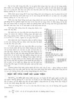
devices was conducted and data gathered are shown in Figure 5.50.
The columns Distance and Average Voltage in the sample data pro-
vided can be used as a look-up table.
Using the average of the voltage measurements for the four samples,
the following graph was produced. The data points indicate the aver-
age values, and the line shows the best fit equation calculated.
The equation derived that best fits the average voltages is given as:
Distance (cm) ϭ 27 ϫ (Voltage) Ϫ1.1. This equation can be used for
calculating the distance to an object by simply entering the voltage
measured and calculating the distance in centimeters. The preceding
formula is provided for reference only; while it is shown to be quite
accurate, part-to-part variation must be considered.
Ambient Light
Tests have shown the GP2D12 to be highly immune to ambient light lev-
els. Incandescent, fluorescent, and natural light do not appear to bother
it. The only instance where we were able to get it to falsely measure was
when a flashlight was pointed directly into the sensor’s receiver; even a
few degrees off center is enough for the sensor to ignore it.
IR Light
The GP2D12 uses a modulated IR beam to guard against false trigger-
ing from the IR component of incandescent, fluorescent, and natural
light. Tests with several kinds of IR remote controls have shown that
even with two or three remotes pointed at the GP2D12, the unit still
functions normally.
Chapter 5 / The Electronics
105
Figure 5.50
Average distance
versus voltage.
PDA 05 5/30/03 11:35 AM Page 105
Laser Light
Tests with a laser pointer had results similar to those with the flash-
light; only a beam aimed straight into the sensor’s receiver would
cause a false reading. If the beam comes from even a few degrees off
center, it has no effect.
Operation
The GP2D12 uses an array of photo diodes (called a position sensitive
detector, or PSD) and some simple optics to detect distance. An IR diode
emits a modulated beam; the beam hits an object and a portion of the
light is reflected back through the receiver optics and strikes the PSD.
CAUTION: The GP2D12 is a precision device. Do not attempt to open
the unit. Doing so will ruin the delicate alignment of the optics. If you
want to open one up, by all means do so, but realize beforehand that
it may not function properly afterward. A block diagram of the
GP2D12 is shown in Figure 5.51.
Overall I found this to be an average range finder for PDA Robot. I
found that the 10-cm starting range and the narrow beam lead to lim-
itations. I will describe them in the chapters on programming the
PIC16F876 and PDAs. I would recommend looking into a sonar range
finder.
PDA Robotics
106
Figure 5.51
GP2D12 block diagram.
PDA 05 5/30/03 11:35 AM Page 106
107
This chapter explains step-by-step how to create the electrical and
mechanical components of PDA Robot.
Creating the Circuit Board
I created the circuit board using the M.G. Chemicals system. The M.G.
Chemicals system allows you to make your own circuit boards quick-
ly and easily. It is perfect for prototyping, hobbyists, and educational
applications. Technicians will be impressed with the high resolution,
while amateurs will be impressed with the simplicity of the system.
I purchased the Photofabrication Kit 416-K to create the PDA Robot
circuit board. It includes the following:
• One 3" ϫ 5" cat. #603 presensitized single-sided PCB
• One 4" ϫ 6" cat. #606 presensitized single-sided printed circuit
board (PCB)
• One 6" ϫ 6" cat. #609 presensitized single-sided PCB
• One 475 ml bottle cat. #418 developer
• One 475 ml bottle cat. #415 ferric chloride
• Two cat. #416-S foam brushes
Building PDA
Robot
6
PDA 06 5/27/03 8:37 AM Page 107
Copyright 2003 by The McGraw-Hill Companies, Inc. Click Here for Terms of Use.
• Plastic development tray
• Rubber gloves
• Instruction sheet
Figure 6.1 shows everything that is included in the kit.
Positive Photofabrication Process Instructions
Setup. Protect surrounding areas from developer and etchant splash-
es. Plastic is ideal for this. Work under safe light conditions. A 40 W
incandescent bulb works well. Important: Do not work under fluores-
cent light. If you do so, you will expose the board, making it unusable.
Just prior to exposure, remove white protective film from the presen-
sitized board. Peel it back carefully.
Exposing Your Board. For best results, use M.G. Chemicals cat.
#416-X exposure kit; however, any inexpensive lamp fixture that will
hold two or more 18" fluorescent tubes is suitable.
Place the presensitized board with the copper side toward the expo-
sure source. Lay positive film artwork onto the presensitized copper
side of the board and position as desired. Place the artwork printed
side down to prevent light leakage through the side of the transparen-
cy. Artwork should have been produced by a 600 dpi or better printer.
PDA Robotics
108
Figure 6.1
Contents of the
Photofabrication Kit
416-K.
PDA 06 5/27/03 8:37 AM Page 108
Use a glass weight to cover the artwork, ensuring that no light will
pass under traces (approx. 3 mm glass thickness or greater works best).
Use a 10-minute exposure time at a distance of 5".
The artwork in Figure 6.3 needs to be reproduced on a transparency and
placed on the presensitized “green” surface of the circuit board. To do
this, either scan the artwork and print, make a high-quality photocopy,
or download the file from www.pda-robotics.com and print using a
photo editor. From the printer options, set the quality to its highest pos-
sible setting. I recommend checking the leads on the components to
ensure that the drill holes are the correct size and every hole lines up.
Important: You must print the image at 100%. If your printer settings
are not correct, the components will not fit. Watch out for the compo-
nents themselves. I found that the higher-priced components fit perfect-
ly, but with some of the less-expensive components, the pad and hole
sizes on the artwork may need to be enlarged or the leads filed or
crimped. This happened with the voltage regulators and L298 chips.
Variations from manufacturer to manufacturer will occur. To increase
the hole sizes, simply load the image into an image editor like
Paintbrush, and draw in white space after increasing the size of the pad.
Be careful when expanding the sizes. You don’t want any of the traces
to touch each other, and it’s good to leave as much space as possible.
After printing the artwork on a good-quality transparency, cut it out
using a utility knife or scissors and put it on the presensitized side
after carefully peeling the protective cover off (see Figures 6.3 and
6.4).
Note: Ensure that the printing on the board in not reversed when plac-
ing on the presensitized side. The lettering “PDA Robotics” should be
shown as printed normally, not reversed.
Chapter 6 / Building PDA Robot
109
Figure 6.2
Fluorescent
exposure.
PDA 06 5/27/03 8:37 AM Page 109
Important: Be sure that no fluorescent lights are on anywhere nearby
when doing this. Place a clear glass or acrylic weight over the board
and transparency and place under the fluorescent light source. Expose
the board.
Developing Your Board. The development process removes any pho-
toresist that was exposed through the film positive to ultraviolet light.
Warning: Developer contains sodium hydroxide and is highly corro-
sive. Wear rubber gloves and eye protection while using it. Avoid con-
PDA Robotics
110
Figure 6.3
Artwork for the circuit board.
PDA 06 5/27/03 8:37 AM Page 110
tact with eyes and skin. Flush thoroughly with water for 15 minutes if
it is splashed in the eyes or on the skin.
Using rubber gloves and eye protection, dilute one part M.G. cat. #418
developer with 10 parts of tepid water (weaker is better than stronger)
in a plastic tray. Immerse the board copper side up into the developer,
and you will quickly see an image appear while you are lightly brush-
ing the resist with a foam brush. This should be completed within one
to two minutes. Immediately neutralize development action by rinsing
the board with water. The exposed resist must be removed from the
board as soon as possible. When you are done with the developing
stage, the only resist remaining will be covering what you want your
circuit to be. Completely remove the rest.
Note: Ensure that the mixture of water and developer is mixed thor-
oughly. If it is not, the traces may wash away when the board comes
in contact with a pocket of highly concentrated developer.
Etching Your Board. For best results, use the 416-E Professional
Etching Process Kit or 416-ES Economy Etching Kit. The most popu-
lar etchant is ferric chloride, M.G. cat. #415, an aqueous solution that
dissolves most metals. Use this solution undiluted, and be sure to
completely cover your board.
Warning: This solution is normally heated up during use, generating
unpleasant and caustic vapors. It is very important to have adequate
ventilation. Use only glass or plastic containers. Keep out of reach of
children. It may cause burns or stain. Avoid contact with skin, eyes,
Chapter 6 / Building PDA Robot
111
Figure 6.4
Cutting out the
circuit board
artwork.
PDA 06 5/27/03 8:37 AM Page 111
or clothing. Store in a plastic container. Wear eye protection and rub-
ber gloves.
Directions: If you use ferric chloride cold, it will take a long time to
etch the board. To speed up etching, heat the solution. A simple way
of doing this is to immerse the ferric chloride bottle or jug in hot water,
adding or changing the water to keep it hot. A thermostat-controlled
crock pot is also an effective way to heat ferric chloride, as are ther-
mostatically controlled submersible heaters—glass-enclosed such as
an aquarium heater. An ideal etching temperature is 50°C (120°F). Be
careful not to overheat it. The absolute maximum working tempera-
ture is approximately 57°C (135°F). The warmer the etch solution, the
faster the boards will etch. Ferric chloride solution can be used over
and over again, until it becomes saturated with copper. As the solution
becomes more saturated, the etching time will increase. Agitation
assists in removing unwanted copper faster. This can be accomplished
by using air bubbles from two aquarium air wands with an aquarium
air pump. Do not use aquarium “air stone.”
The etching process can be assisted by brushing the unwanted resist
with a foam brush while the board is submerged in the ferric chloride.
I found that rocking the board back and forth in the pan by holding it
by the edges with rubber gloves on works well. The ferric chloride can
be kept warm by placing the glass basin on a stove element set to low.
Turn on the fume hood to expel any fumes.
After the etching process is completed, wash the board thoroughly
under running water. Do not remove the remaining resist protecting
your circuit or image. It protects the copper from oxidation.
PDA Robotics
112
Figure 6.5
Circuit board ready
for etching.
PDA 06 5/27/03 8:37 AM Page 112
Removal of resist is not necessary when soldering components to the
board. By leaving the resist on, you protect the circuit from oxidation.
Tin plating the board is not necessary. In soldering, the heat disinte-
grates the resist underneath the solder, resulting in an excellent bond.
Drilling Out the Circuit Board. Once the board is dry, drill out the
holes using the appropriate drill bits. Be sure that the bit is in straight
and that you hit the hole dead center. Figure 6.6 shows the main board
being drilled out. Figure 6.7 shows the ribbon connector holes on a
transponder circuit board.
Cutting the Board. The board can be cut into the three sections by
repeatedly scoring with a utility knife, using a hacksaw, or using a
band saw. Note: Only one of the infrared (IR) transceiver boards is
required for this project. Figure 6.8 shows where the board should
be cut.
Placing and Soldering the Components. The boards are now ready
to have the components soldered into place. The components go onto
the topside of the board (opposite side from the traces), with the
exception of the TFDS4500 on the transceiver circuit board.
Chapter 6 / Building PDA Robot
113
Figure 6.6
Drilling the main
board.
PDA 06 5/27/03 8:37 AM Page 113
PDA Robotics
114
Figure 6.8
Cut the boards on the dotted lines.
Figure 6.7
Dead center drill.
PDA 06 5/27/03 8:37 AM Page 114
Parts Lists
The Main Board. Parts for the main board include:
• One PIC16F876 microcontroller
• One 28-pin DIP IC socket (or 2 18-pin DIP IC sockets with one cut
down)
• One MCP2150 IrDA protocol chip
• One 18-pin DIP IC socket
• One L7805ACV voltage regulator
• One 8-pin DIP switch
• One 11.0592 MHz crystal
• One 20.0000 MHz crystal
• One 3.9 mm (.156") Molex wire connectors
• One Molex 3.9 mm 2P header with ramp connects
• Two 6-post 2.5 mm DIP headers
• Two IDC6F DIP connector with key
• One Red LED
• Three 1 K resistor
• Two 47R 1/4 W resistors
• One 4.7 UF tantalum capacitor
• Six 22 pF capacitors
• One 1-pin
• 8" of six-wire ribbon cable
The Motor Controller. Parts for the motor controller include:
• One L298N dual bridge driver
• Four 3.9 mm (.156") Molex wire connectors
• Four Molex 3.9 mm 2P header with ramp connects
• Two 6-post 2.5 mm DIP headers
Chapter 6 / Building PDA Robot
115
PDA 06 5/27/03 8:37 AM Page 115
• Two IDC6F DIP connector with key
• Eight 4007 746 diodes
• Three .1 UF capacitors (or higher)
The IR Transceiver. Parts for the IR transceiver include:
• One TFDS4500
• One 6-post 2.5 mm DIP headers
• One IDC6F DIP connector with key
• 6" of six-wire ribbon cable
Range Finder and Attachments. Parts for the range finder and
attachments include:
• One GP2D12 distance measuring system with cable and attach-
ments (AIRRS @ www.hvwtech.com )
• Two .156" wire connectors
The Body. Parts for the body include:
• Aluminum: 8" ϫ 6" ϫ 1/16" (main platform)
• Aluminum: 7" ϫ 5 1/4" (top platform) ϫ 1/16"
• Aluminum: 1" ϫ 1/2" ϫ 1/4" (accessory mount)
• Two Tamiya six-speed geared motors (www.hvwtech.com)
• Three Tamiya wheel sets
• Four 1" L-brackets
• Five 2" 4-40 hex spacers
• Eight 1/2" 4-40 hex spacers
• One 9 V battery connector
• One 6 V battery pack (4 ϫ 1.5 V AA)
• 6" of Velcro with self-basting adhesive (secure batteries)
• 1' of double-sided Velcro (secure PDA)
• Package of 50 4-40 1/4" nuts, bolts, and washers.
PDA Robotics
116
PDA 06 5/27/03 8:37 AM Page 116
Placing and Soldering the
Main Board Components
Figures 6.9 to 6.11 show the placement of the parts. The following
numbers correspond to those on the main circuit board. Place and sol-
der the parts.
1. Molex 3.9 mm 2P header with ramp connects to Molex 156" (3.9
mm) wire connector
2. L7805ACV voltage regulator
3. 22 pF capacitors
4. 1 K resistors
5. Red LED
6. 47R 1/4 W resistors
7. 4.7 UF tantalum capacitor
Chapter 6 / Building PDA Robot
117
Figure 6.9
Main board parts placement.
PDA 06 5/27/03 8:37 AM Page 117