MEMS and Microstructures in Aerospace Applications - Robert Osiander et al (Eds) Part 3 ppsx
Bạn đang xem bản rút gọn của tài liệu. Xem và tải ngay bản đầy đủ của tài liệu tại đây (1.51 MB, 18 trang )
BBBBBBBBBBBBBBBBBBBBBBBB
BBBBBBBBBBBBBBBBBBBBBBBB
BBBBBBBBBBBBBBBBBBBBBBBB
Single Crystal Silicon
(a) Implant Boron in Single Crystal Silicon wafer
<100>
(b) Deposit and Pattern Silicon Dioxide Etch Mask
SiO
2
Mask
<111>
(c) KOH Etch
FIGURE 3.5 Boron-doped silicon used to form features or an etch stop.
TABLE 3.2
Common Crystalline Silicon Etchants’ Selectivity and Etch Rates
Etchant Etch Rate
18HF þ4HNO
3
þ 3Si ! 2H
2
SiF
6
þ 4NO þ 8H
2
O Nonselective
Si þH
2
O þ2KOH ! K
2
SiO
3
þ 2H
2
{1 0 0} 0.14 m/min
{1 1 1} 0.0035 m/min
SiO
2
0.0014 m /min
SiN
4
not etched
Ethylene diamine pyrocatechol (EDP) {1 0 0} 0.75 m/min
{1 1 1} 0.021 m/min
SiO
2
0.0002 m /min
SiN
4
0.0001 m /min
Tetramethylammonium hydroxide (TMAH) {100} 1.0 m/min
{1 1 1} 0.029 m/min
SiO
2
0.0002 m /min
SiN
4
0.0001 m /min
Osiander / MEMS and microstructures in Aerospace applications DK3181_c003 Final Proof page 43 1.9.2005 8:59pm
MEMS Fabrication 43
© 2006 by Taylor & Francis Group, LLC
flow necessary for the reaction to occur. The p–n junction can be formed on a p-type
silicon wafer with an n-type region diffused or implanted with an n-type dopant
(e.g., phosphorus, arsenic) to a prescribed depth. With the p–n junction reverse
biased, the p-type silicon will be etched because a protective oxide layer cannot be
formed and the etch will stop on the n-type material.
3.4.2 PLASMA ETCHING
Plasma etching offers a number of advantages compared to wet etching:
.
Easy to start and stop the etch process
.
Repeatable etch process
.
Anisotropic etches
.
Few particulates
Plasma etching includes a large variety of etch processes and associated chemistries
that involve varying amounts of physical and chemical attack. The plasma provides
a flux of ions, radicals, electrons, and neutral particles to the surface to be etched.
Ions produce both physical and chemical attack of the surface, and the radicals
contribute to chemical attack.
(b) Completed Structure
+
Diffused or
implanted n-type
silicon region
Electrode
Etchant
V
Mask
Container
Container
(a) Electrochemical Etch Schematic
P-type silicon
FIGURE 3.6 Electrochemical etch stop process schematic.
Osiander / MEMS and microstructures in Aerospace applications DK3181_c003 Final Proof page 44 1.9.2005 8:59pm
44 MEMS and Microstructures in Aerospace Applications
© 2006 by Taylor & Francis Group, LLC
The details and types of etch chemistries involved in plasma etching are varied and
quite complex. This topic is too voluminous to be discussed in detail here, but there
exist a number of excellent references on this subject.
15
The proper choice of these
chemistries produces various etch rates and selectivity of material etch rates, which is
essential to the integration of processes to produce microelectronics or MEMS devices.
Fluoride etch chemistries is one of the most widely studied for silicon etches. Equations
(3.3), (3.4), and (3.5) illustrate some of the fluoride reactions involved in the etching of
silicon, silicon dioxide, and silicon nitride, respectively. There are a number of feed
gases that can produce the free radicals involved in these reactions:
Si þ4F
Ã
! SiF
4
(3:3)
3SiO
2
þ 4CF
þ
3
! 2CO þ2CO
2
þ 3SiF
4
(3:4)
Si
3
N
4
þ 12F
Ã
! 3SiF
4
þ 2N
2
(3:5)
The anisotropy of the plasma etch can be increased by the formation of nonvolatile
fluorocarbons that deposit on the sidewalls as seen in Figure 3.7. This process is
Initial
deposition
Deposition
Deposit and
pattern the
mask
Initial
etch
Neutral
Volatile etch product
Ion
Next
etch
cycle
Neutral
Volatile etch products
Ion
Nonvolatile sidewall deposits
FIGURE 3.7 Schematic of sidewall polymerization to enhance anisotropic etching.
Osiander / MEMS and microstructures in Aerospace applications DK3181_c003 Final Proof page 45 1.9.2005 8:59pm
MEMS Fabrication 45
© 2006 by Taylor & Francis Group, LLC
called polymerization and is controlled by the ratio of fluoride to carbon in the
reactants. The sidewall deposits produced by polymerization can only be removed
by physical ion collisions. Etch products from the resist masking are also involved
in the polymerization.
Etch endpoint detection is important in controlling the etch depth or minimizing
the damage to underlying films. Endpoint detection is accomplished by analysis of
the etch effluents or spectral analysis of the plasma glow discharge to detect.
The type of plasma etches include reactive ion etching (RIE), high-density
plasma etching (HDP), and deep reactive ion etching (DRIE). RIE utilizes low-
pressure plasma. Chlorine (Cl)-based plasmas are commonly used to etch silicon,
GaAs, and Al. RIE may damage the material due to the impacts of the ions. The
damage can be mitigated by annealing at high temperatures. HDP etches utilize
magnetic and electric fields to dramatically increase the distance that free electrons
can travel in the plasma. HDP etches have good selectivity of Si to SiO
2
and
resist. The DRIE etch cycles between the etch chemistry and deposition of the
sidewall polymer, which enables the high aspect ratio and vertical sidewalls attain-
able with this process.
16
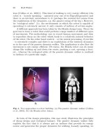
Figure 3.8 shows two sample applications of bulk micromachining utilizing
DRIE to produce deep channels and an electrostatic resonator.
3.5 SACRIFICIAL SURFACE MICROMACHINING
The basic concept of surface micromachining fabrication process has had its roots
as far back as in the 1950s and 1960s with electrostatic shutter arrays
17
and a
resonant gate transistor.
11
However, it was not until the 1980s that surface micro-
machining utilizing the microelectronics toolset received significant attention.
200 µm
(a) Channels (b) Resonator
FIGURE 3.8 Bulk micromachined channels and resonator. (Courtesy: Sandia National
Laboratories.)
Osiander / MEMS and microstructures in Aerospace applications DK3181_c003 Final Proof page 46 1.9.2005 8:59pm
46 MEMS and Microstructures in Aerospace Applications
© 2006 by Taylor & Francis Group, LLC
Howe and Muller
18
provided a basic definition of polycrystalline silicon surface
micromachining, and Fan et al.
19
illustrated an array of mechanical elements such
as fixed-axle pin joints, self-constraining pin joints, and sliding elements. Pister
et al.
20
demonstrated the design for microfabricated hinges, which enable the
erection of optical mirror elements.
Surface micromachining is a fabrication technology based upon the deposition,
patterning, and etching of a stack of materials upon a substrate. The materials
consist of alternating layers of a structural material and a sacrificial material. The
sacrificial material is removed at the end of the fabrication process via a release
etch, which yields an assembled mechanical structure or mechanism. Figure 3.9
illustrates the fabrication sequence for a cantilever beam fabrication in a surface
micromachine process that has two structural layers and one sacrificial layer.
Surface micromachining uses the planar fabrication methods common to the
microelectronics industry. The tools for depositing alternating layers of structural
and sacrificial materials, photolithographical patterning, and etching the layers have
their roots in the microelectronics industry. Etches of the structural layers define the
shape of the mechanical structure, while the etching of the sacrificial layers define
the anchors of the structure to the substrate and between structural layers. Depos-
ition of a low-stress structural layer is a key goal in a surface micromachine process.
From a device-design standpoint, it is preferable to have a slightly tensile average
residual stress with minimal or zero residual stress gradient, which eliminates the
design consideration of structural buckling. The stress in a thin film is a function of
the deposition conditions such as temperature. A postdeposition anneal is frequently
used to reduce the layer stress levels. For polysilicon the anneal step can require
several hours at 11008C.
Patterned first
structural layer
Patterned first
sacrificial layer
Substrate and
isolation layers
FIGURE 3.9 Surface micromachined cantilever beam with underlying electrodes showing
the effect of topography induced by conformal layers.
Osiander / MEMS and microstructures in Aerospace applications DK3181_c003 Final Proof page 47 1.9.2005 8:59pm
MEMS Fabrication 47
© 2006 by Taylor & Francis Group, LLC
Polycrystalline silicon (polysilicon) and silicon dioxide are a common set of
structural and sacrificial materials, respectively, used in surface micromachining.
The release etch for this situation is HF, which readily etches silicon dioxide but
minimally attacks the polysilicion layers. A number of different combinations of
structural, sacrificial materials and release etches have been utilized in surface
micromachining processes. Table 3.3 summarizes a sample of surface microma-
chining material systems that have been utilized in commercial and foundry pro-
cesses. Material system selection depends on several issues such as the structural
layer mechanical properties (e.g., residual stress, Young’s modulus, hardness, etc.)
or the thermal budget required in the surface micromachining processes, which may
affect additional processing necessary to develop a product.
Even though surface micromachining leverages the fabrication processes and
tool set of the microelectronics industry, there are several distinct differences and
challenges shown in Table 3.4. The surface micromachine MEMS devices are
generally larger and they are composed of much thicker films than microelectronic
devices. The repeated deposition and patterning of the thick films used in surface
micromachining will produce a topography of increasing complexity as more layers
are added to the process. Figure 3.9 shows the topography induced on an upper
structural layer by the patterning of lower levels caused by the conformal films
deposited by processes such as chemical vapor deposition (CVD). Figure 3.10
shows a scanning electron microscopic image of this effect in an inertial sensor
made in a two-level surface micromachine process.
In addition to the topography induced in the higher structural levels by the
patterning of lower structural and sacrificial layers, there are two significant process
difficulties encountered. The first difficulty results from the anisotropic plasma
etch used for the definition of the layer features to attain vertical sidewalls. The
topography in the layer will inhibit the removal of material in the steps of the
topographical features. This is illustrated in Figure 3.11, which shows there is an
increased vertical layer height at the topographical steps that prevents removal of
TABLE 3.3
Example Surface Micromachining Technologies
Material Systems
Structural Sacrificial Release Application
PolySi SiO
2
HF SUMMiT Ve
SiN polySi XeF
2
GLVe
Al Resist Plasma etch TI DMDe
SiC PolySi XeF
2
MUSICe
Note: SUMMiTe — Sandia Ultra-planar, Multi-level MEMS Technology
GLVe — Grating Light Valve (Silicon Light Machines)
TI DMDe — Digital Mirror Device (Texas Instruments)
MUSICe — Multi User Silicon Carbide (FLX micro)
Osiander / MEMS and microstructures in Aerospace applications DK3181_c003 Final Proof page 48 1.9.2005 8:59pm
48 MEMS and Microstructures in Aerospace Applications
© 2006 by Taylor & Francis Group, LLC
SUMMiTe (Sandia National Laboratories, Albuquerque, New Mexico), before and
after CMP, was included in the process. In addition to solving the fabrication issues
of topography, the use of CMP also aids in realizing designs without range of
motion and interference constraints imposed by topography issues. CMP will also
aid in the development of MEMS optical devices by enhancing the optical quality of
surface micromachined MEMS mirrors.
24
The release etch is the last step in the surface micromachine fabrication
sequence. For a polysilicon surface micromachine process, the release etch involves
a wet etch in HF to remove the silicon dioxide sacrificial layers. The removal of the
sacrificial layers will yield a mechanically free device capable of motion. For very
(a) Example of a conformable layer (b) Example of topography removed
by Chemical Mechanical Polishing
FIGURE 3.13 Example of a linkage fabricated in SUMMiTe with and without CMP.
(Courtesy: Sandia National Laboratories.)
2.0 µm SACOX3 (CMP)
0.4 µm DIMPLE3 Gap
0.3 µm MMPOLY0
0.80 µm Silicon Nitride
1.5 µm MMPOLY2
0.3 µm SACOX2
0.63 µm Thermal SiO
2
Substrate
6 inch wafer, <1 00>, n-type-
2.25 µm MMPOLY3
1.0 µm MMPOLY1
2.0 µm SACOX4 (CMP)
2.0 µm SACOX1
0.5 µm DIMPLE1 Gap
2.25 µm MMPOLY4
0.2 µm DIMPLE4 Gap
FIGURE 3.14 SUMMiT Ve layers and features.
Osiander / MEMS and microstructures in Aerospace applications DK3181_c003 Final Proof page 51 1.9.2005 8:59pm
MEMS Fabrication 51
© 2006 by Taylor & Francis Group, LLC
long or wide structures, etch-release holes are frequently incorporated into the
structural layers to provide access for HF to the underlying sacrificial silicon
dioxide. This will reduce the etch-release process time. Since the MEMS device
is immersed in a liquid during the release etch, an issue is the adhesion and stiction
of the MEMS layers upon removal from the liquid release etchant.
25
Since poly-
silicon surfaces are hydrophilic the removal of liquids from the MEMS device can
be problematic. Surface tension of the liquid between the MEMS layers will
produce large forces, pulling the layers together. Stiction of the MEMS layers
after the release etch can be addressed in several ways:
.
Making the MEMS device very stiff to resist the surface tension forces
.
Fabricating a bump (i.e., dimple) on the MEMS surfaces, which will prevent
the layers from coming into large area contact
.
Using a fusible link to hold the MEMS device in place during the release etch,
which can be mechanically or electrically removed subsequently
26
.
Using a release process, which avoids the liquid meniscus during drying, such
as supercritical carbon dioxide drying
27
or freeze sublimation
28
.
Use a release process that will make the surface hydrophobic, by using self-
assembled monolayer (SAM) coatings.
29
It has been reported that SAM
coatings also have the affect of reducing friction and wear
3.5.1 SUMMiT Ve
An example of a surface micromachined MEMS fabrication process is SUMMiT
(Sandia Ultra-planar, Multi-level MEMS Technology), a state-of-the-art five-level
surface micromachine process developed by Sandia National Laboratories.
30,31
SUMMiT processing utilizes standard IC processes, which are optimized for the
thicker films required in MEMS applications. Low-pressure chemical vapor
deposition (LPCVD) is used to deposit the polysilicon and silicon dioxide films.
Optical photolithography is utilized to transfer the designed patterns on the mask
to the photosensitive material that is applied to the wafer (e.g., photoresist or
resist). Reactive ion etches are used to etch the defined patterns into the thin
films of the various layers. A wet chemical etch is also used to define a hub
feature, as well as the final release etch of the SUMMiT process. Figure 3.14
schematically shows the layers and features in the SUMMiT V process. The
SUMMiT V process uses 14 photolithography steps and masks to define the required
features. Table 3.5 lists the layer and mask names and a summary of their use.
The SUMMiT fabrication process begins with a bare n-type, <100> silicon
wafer. A 0.63 mm layer of SiO
2
is thermally grown on the bare wafer. This layer
of oxide acts as an electrical insulator between the single-crystal silicon substrate
and the first polycrystalline silicon layer (MMPOLY0). A 0.8 mm thick layer of
low-stress silicon nitride (SiN
x
) is deposited on top of the oxide layer. The nitride
layer is an electrical insulator, but it also acts as an etch stop protecting the
underlying oxide from wet etchants during processing. The nitride layer can
be patterned with the NITRIDE_CUT mask to establish electrical contact with the
Osiander / MEMS and microstructures in Aerospace applications DK3181_c003 Final Proof page 52 1.9.2005 8:59pm
52 MEMS and Microstructures in Aerospace Applications
© 2006 by Taylor & Francis Group, LLC
is conformable and will deposit on the inside wall of the hub structure. The
thickness of SACOX2 defines the clearance of the hub structure. SACOX2 can
also be used as a hard mask to define MMPOLY1 using the subsequent etch that
also defines MMPOLY2.
Upon completion of the SACOX2 deposition, pattern, and etch, a 1.5-mm thick
layer of doped polysilicon, MMPOLY2 is deposited. Any MMPOLY2 layer ma-
terial that is deposited directly upon MMPOLY1 (i.e., not separated by SACOX2)
will be bonded together. Following the MMPOLY2 deposition, an anisotropic
reactive ion etch is performed to etch MMPoly2 and composite layers of
MMPOLY1 and MMPOLY2 (laminated together to form a single layer 2.5-mm
thick). The MMPOLY2 etch will stop on silicon dioxide, hence MMPOLY1 will be
protected by any SACOX2 on top of MMPOLY1 and the SACOX2 layer can be
used as a hard mask to define a pattern in MMPOLY1.
At this point in the SUMMiT V process all the layers have been conformable
(i.e., assume the shape of the underlying patterned layers). To enable the addition
of subsequent structural and sacrificial levels without the fabrication and design
constraints of the conformable layers, CMP is used to planarize the sacrificial
oxide layers. With the MMPOLY2 etch complete, approximately 6 mm of TEOS
(tetraethoxysilane) silicon dioxide (SACOX3) is deposited. CMP is used to planar-
ize the oxide to a thickness of about 2 mm above the highest point of MMPOLY2.
Following planarization, SacOx3 is patterned and etched to provide dimples
and anchors to the MMPOLY2 layer using the DIMPLE3_CUT and SACOX3_
CUT masks, respectively. The DIMPLE3_CUT etch is performed by etching all
the way through the SACOX3 layer, stopping on MMPOLY2. Then 0.4 mmof
silicon is deposited to backfill the dimple hole to provide the 0.4 mm standoff
distance. The processing of the DIMPLE3 feature will provide a repeatable standoff
distance.
A2-mm thick layer of doped poly (MMPoly3) is deposited on the CMP
planarized SACOX3 layer. The MMPOLY3 layer will be flat and not have the
topography due to the patterning of the underlying layers. This will ease design
constraint on the higher levels and enhance the use of MMPOLY3 and MMPOLY4
layers as mirror surfaces in optical applications. The MMPOLY3 layer is patterned
and etched using the MMPOLY3 mask.
The processing for the SACOX4 and MMPOLY4 layers proceeds using the
SACOX4_CUT, DIMPLE4_CUT, and MMPOLY4 mask in an analogous fashion to
the SACOX3 and MMPOLY3 layers, except that the DIMPLE4 standoff distance is
0.2 mm.
Release and drying of the SUMMiT V die are the final fabrication steps. The
device is released by etching all the exposed silicon dioxide away with a 100:1
HF:HCl wet etch. Following the wet release etch, a drying process can be employed
using either simple air evaporation, supercritical CO
2
drying,
27
or CO
2
freeze
sublimation.
28
The choice of the drying process will depend upon the design of
the particular devices. Structures that are very stiff will be less sensitive to the
surface tension forces, and they can be processed by simple air drying. Supercritical
CO
2
drying processing for large devices is a better option.
Osiander / MEMS and microstructures in Aerospace applications DK3181_c003 Final Proof page 54 1.9.2005 8:59pm
54 MEMS and Microstructures in Aerospace Applications
© 2006 by Taylor & Francis Group, LLC
Figure 3.15 illustrates the SUMMiT V masks and layers to fabricate a post
containing all the structural layers. For this particular structure the dimple and the
hub capabilities of SUMMiT are not utilized.
The SUMMiT V sacrificial surface micromachine fabrication process is capable
of fabricating complex mechanisms and actuators. The ability to fabricate a low-
clearance hub enables the rotary mechanisms and gear reduction systems shown in
Figure 3.16. Figure 3.17 shows a vertically erected mirror that is held in place by
elastic snap hinges. The vertical mirror is mounted upon a rotationally indexable
table driven by an electrostatic comb drive actuator. SUMMiT V has also been used
to fabricate large arrays of devices that are enabled by the fact that surface micro-
machined devices are assembled when they are fabricated.
3.6 INTEGRATION OF ELECTRONICS AND MEMS
TECHNOLOGY
The integration of electronic circuitry with MEMS technology becomes essential
for sensing applications, which require increased sensitivity (e.g., Analog Devices
ADXL accelerometers
32
), or actuation applications, which require the control of
large arrays of MEMS devices (e.g., Texas Instruments Digital Mirror Device
[DMD
1
]
33
). For sensor applications the packaging integration of a MEMS device
and an electronic ASIC becomes unacceptable when the parasitic capacitances and
wiring resistances impact sensor performance (i.e., RC time constants of the
integrated MEMS system are significant). For actuation applications such as a
large array of optical devices that require individual actuation and control circuitry,
a packaging solution becomes untenable with large device count.
FIGURE 3.15 Masks and cross-section of a post composed of anchored layers.
Osiander / MEMS and microstructures in Aerospace applications DK3181_c003 Final Proof page 55 1.9.2005 8:59pm
MEMS Fabrication 55
© 2006 by Taylor & Francis Group, LLC
Of the three MEMS fabrication technologies previously discussed, surface
micromachining is the most amenable to integration with electronics to form an
integration of electonics and MEMS technology (IMEMS) process. There are
several challenges to the development of an IMEMS process:
.
Large vertical topologies: Microelectronic fabrication requires planar sub-
strates due to the use of precision photolithographic processes. Surface
micromachine topologies can exceed 10 mm due to the thickness of the
various layers.
.
High-temperature anneals: The mitigation of the residual stress of the sur-
face micromachine structural layers can require extended period time at high
temperatures (such as several hours at 11008C for polysilicon). This would
have adverse effects due to the thermal budget of microelectronics that is
limited due to dopant diffusion and metallization.
There are three strategies for the development of an IMEMS process.
34
.
Microelectronics first: This approach overcomes the planarity constraint
imposed by the photolithographic processes by building the microelectronics
before the nonplanar micromechanical devices. The need for extended
high temperature anneals is mitigated by the selection of MEMS materials
(e.g., aluminum, amorphous diamond
35
), and selection of the microelectronic
metallization (e.g., tungsten instead of aluminum), which make the MEMS
and microelectronic processing compatible. Examples of this IMEMS ap-
proach include an all-tungsten CMOS process that was developed by
researchers at the Berkeley Sensor and Actuator Center
36
seen in Figure
3.18. The TI DMD (Texas Instruments Incorporated, Dallas, TX)
33
uses the
microelectronics first approach and utilizes an aluminum structural layer
MEMS and photoresist sacrificial layer MEMS, which enables low-tempera-
ture processing.
.
Interleave the microelectronics and MEMS fabrication: This approach
may be the most economical for large-scale manufacturing since it optimizes
and combines the manufacturing processes for MEMS and microelectronics.
However, this requires extensive changes to the overall manufacturing flow
in order to accommodate the changes in the microelectronic device or the
MEMS device. Analog devices has developed and marketed an accelerometer
and gyroscope that illustrates the viability and commercial potential of the
interleaving integration approach.
32
.
MEMS fabrication first: This approach fabricates, anneals, and planarizes
the micromechanical device area before the microelectronic devices are
fabricated, which eliminates the topology and thermal processing constraints.
The MEMS devices are built in a trench, which is then refilled with oxide,
planarized, and sealed to form the starting wafer for the CMOS processing
as seen in Figure 3.19. This technology was targeted for inertial sensor
Osiander / MEMS and microstructures in Aerospace applications DK3181_c003 Final Proof page 57 1.9.2005 9:00pm
MEMS Fabrication 57
© 2006 by Taylor & Francis Group, LLC
applications. Prototypes were designed by the Berkeley Sensor and Actuator Center
(BSAC), University of California, and fabricated by Sandia National Laboratories
shown in Figure 3.20.
3.7 ADDITIONAL MEMS MATERIALS
In addition to silicon-based materials and electroplated metals that have been
discussed for use in MEMS technologies, a number of other materials are available,
which may have unique properties that enable particular applications. For example,
the high-temperature properties of silicon carbide, the hardness of diamond and
silicon carbide, or the low deposition temperatures of silicon–germanium alloys and
diamond.
3.7.1 SILICON CARBIDE
Silicon carbide (SiC) has outstanding mechanical properties, particularly at high
temperatures. Silicon is generally limited to lower temperatures due to a reduction
in the mechanical elastic modulus above 6008C and a degradation of the electrical
pn-junctions above 1508C. Silicon carbide is a wide bandgap semiconductor (2.3–
3.4 eV), which suggests the promise of high-temperature electronics.
37
It also has
outstanding mechanical properties of hardness, elastic modulus, and wear resist-
ance,
38
as seen in Table 3.6. SiC does not melt but sublimes above 18008C, and it
Z-Axis Gyro
XYZ
Accelerometer
1 cm
XY-Axis
Gyro
FIGURE 3.20 Inertial measurement unit fabricated in the MEMS first approach to MEMS-
microelectronics process integration method. Designed at University of California, Berkeley,
Berkeley Sensor Actuator Center. Fabricated by Sandia National Laboratories.
Osiander / MEMS and microstructures in Aerospace applications DK3181_c003 Final Proof page 60 1.9.2005 9:00pm
60 MEMS and Microstructures in Aerospace Applications
© 2006 by Taylor & Francis Group, LLC
Ge
x
an attractive micromachining material for monolithic integration with micro-
electronics, which requires a low thermal budget.
44
Also, a surface micromachining process can be implemented utilizing poly-
Si
1Àx
Ge
x
as the structural film, poly-Ge as the sacrificial film with a release etch of
hydrogen peroxide when x < 0.4. Poly-Ge can be deposited as a highly conformable
material that enables many MEMS structures.
3.7.3 DIAMOND
Diamond and hard amorphous carbon form a promising class of materials that have
extraordinary properties, which promote new applications for MEMS devices. The
various amorphous forms of carbon such as amorphous diamond (aD), tetrahedral
amorphous carbon (ta-C), and diamond-like carbon (DLC) have hardness and
elastic modulus properties that approach crystalline diamond, which has the highest
hardness (~100 GPa) and elastic modulus (~1100 GPa) of all materials.
45
The
appeal of this class of materials for MEMS designers is the extreme wear resistance,
hydrophobic surfaces (i.e., stiction resistance), and chemical inertness. Recent
progress has been achieved in the area of surface micromachining and mold-
based processes
46,47
and a number of diamond MEMS devices have been demon-
strated.
48,49
The use of diamond films in MEMS is still in the research stages.
Recent progress in stress relaxation of the diamond films
50,51
at 6008C has been
essential to the development of diamond as a MEMS material.
3.7.4 SU-8
EPON SU-8 (Shell Chemical) is a negative, thick, epoxy-photoplastic high aspect
ratio resist for lithography.
52
This UV-sensitive resist can be spin coated in a
conventional spinner to thicknesses ranging from 1 to 300 mm. Up to 2-mm
thicknesses can be obtained with multilayer coatings. SU-8 has very suitable
mechanical and optical properties and chemical stability; however, it has the
disadvantages of adhesion selectivity, stress, and resists stripping. SU-8 adhesion
is good on silicon and gold, but on materials such as glass, nitrides, oxides, and
other metals the adhesion is poor. In addition, the thermal expansion coefficient
mismatch between SU-8 and silicon or glass is large.
SU-8 has been applied to MEMS fabrication
52,53
for plastic molds or electro-
plated metal micromolds. Also SU-8 MEMS structures have been used for micro-
fluidic channels, and biological applications.
54
3.8 CONCLUSIONS
Three categories of micromachining fabrication technologies have been presented;
bulk micromachining, LIGA, and sacrificial surface micromachining.
Bulk micromachining is primarily a silicon-based technology that employs wet
chemical etches and reactive ion etches to fabricate devices with high aspect ratio.
Control of the bulk micromachining etches with techniques such as etch stops and
Osiander / MEMS and microstructures in Aerospace applications DK3181_c003 Final Proof page 62 1.9.2005 9:00pm
62 MEMS and Microstructures in Aerospace Applications
© 2006 by Taylor & Francis Group, LLC
material selectivity is necessary to make useful devices. Commercial applications
utilizing bulk micromachining are available such as accelerometers and ink-jet
nozzles.
LIGA is a fabrication technology that utilizes x-ray synchrotron radiation, a
thick resist material and electroplating technology to produce high aspect ratio
metallic devices.
Surface micromachining is a technology that uses thick films and processes
from the microelectronic industry to produce devices. Surface micromachining
employs two types of materials, a sacrificial material and a structural material, in
alternating layers. A release process removes the sacrificial material in the last step
in the process, which produces free function structural devices. Surface microma-
chining enables large arrays of devices since no assembly is required. Surface
micromachining is also integratable with microelectronic for sensing and control.
Two notable commercial applications of surface micromachining are the TI DMD
and the Analog Devices ADXL accelerometers.
New materials are being developed to enhance MEMS applications. For ex-
ample, silicon carbide is a hard, high-temperature material, which can withstand
harsh environments. Silicon–germanium and diamond are materials that can be
deposited at low temperatures, which enable increased MEMS process flexibility.
SU-8 is an epoxy photo resin that can be used to produce high aspect ratio channels
and molds.
REFERENCES
1. Sobel, D., Longitude, The True Story of a Lone Genius Who Solved the Greatest
Scientific Problem of His Time, Penguin Books, New York, 1995.
2. Shockley, W., A unipolar field-effect transistor, Proceedings of IRE, 40, 1365, 1952.
3. Hoerni, J.A., Planar silicon transistors and diodes, Proceedings of the IRE Electron
Devices Meeting, Washington, D.C., October 1960.
4. Hoerni, J.A., Method of Manufacturing Semiconductor Devices, U.S. Patent 3,025,589,
issued March 20, 1962.
5. Feynman, R.P., There’s plenty of room at the bottom, Engineering and Science (Cali-
fornia Institute of Technology) February 1960, 22–36.
6. Feynman, R.P., There’s plenty of room at the bottom, JMEMS, 1(1), March 1992.
7. Feynman, R.P., There’s plenty of room at the bottom, />feynman.html
8. Regis, E., Nano: The Emerging Science of Nanotechnology, Little Brown and Company,
New York, 1995.
9. Maluf, N., An Introduction to Microelectromechanical Systems Engineering, Artech
House, Inc., Norwood, MA, 2000.
10. Smith, C.S., Piezoresistive effect in germanium and silicon, Physical Reviews, April 4,
1954.
11. Nathanson, H.C., et al., The resonant gate transistor, IEEE Transactions of Electronic
Devices ED-14, 117–133, 1967.
12. Petersen, K.E., Silicon as a mechanical material, Proceedings of the IEEE, 70(5), May
1982, 420–457.
Osiander / MEMS and microstructures in Aerospace applications DK3181_c003 Final Proof page 63 1.9.2005 9:00pm
MEMS Fabrication 63
© 2006 by Taylor & Francis Group, LLC
13. Becker, E.W., et al., Fabrication of microstructures with high aspect ratios and great
structural heights by synchrotron radiation lithography, galvanoforming, and plastic
molding (LIGA process), Microelectronic Engineering, 4, 1986, 35.
14. Kovacs, G.T.A., Maluf, N.I., and Petersen, K.E., Bulk micromachining of silicon,
Proceedings of IEEE, 86(8), 1536–1551, August 1998.
15. Shul, R.J. and Pearton, S.J., Handbook of Advanced Plasma Processing Techniques,
Springer, New York, 2000.
16. US Patent 5,501,893, Method of Anisotropically Etching Silicon, Laermer, F., Schlp, A.,
Robert Bosch GmbH, issued March 26, 1996.
17. US Patent 2,749,598, Method of Preparing Electrostatic Shutter Mosaics, filed February
1, 1952, issued June 12, 1956.
18. Howe, R.T. and Muller, R.S., Polycrystalline silicon micromechanical beams,
Journal of Electrochemical Society: Solid-State Science and Technology, 103(6),
1420–1423.
19. Fan, L S., Tai, Y C., and Muller, R.S., Integrated movable micromechanical structures
for sensors and actuators, IEEE Transactions of Electronic Devices, 35(6), 724–730,
1988.
20. Pister, K.S.J., et al., Microfabricated hinges, Sensors and Actuators A, 33, 249–256,
1992.
21. Patrick, W., et al., Application of chemical mechanical polishing to the fabrication of
VLSI circuit interconnections, Journal of Electrochemical Society, 138, 1778–1784.
22. Nasby, R.D., et al., Application of chemical mechanical polishing to planarization of
surface micromachined devices, Solid State Sensor and Actuator Workshop, Hilton Head
Is., SC, 48–53.
23. U.S. Patent 5,804,084, issued September 8, 1998, Use of Chemical Mechanical Polishing
in Micromachining, Nasby, R.D., et al.
24. Yasseen, A., et al., Diffraction grating scanners using polysilicon micromotors, Proceed-
ings of the 8th International Conference on Solid — State Sensors and Actuators, and
Eurosensors IX, 1, Stockholm, Sweden, 206–209, 1995.
25. Legtenberg, R., Elders, J., and Elwenspoek, M., Stiction of surface microstructures
after rinsing and drying: model and investigation of adhesion mechanisms, Proceedings
of the 7th International Conference of Solid State Sensors and Actuators, 198–201, 1993.
26. Fedder, G.K. and Howe, R.T., Thermal assembly of polysilicon microstructures, Pro-
ceedings Microelectro Mechanical Systems ’89, 63–68.
27. Mulhern, G.T., Soane, D.S. and Howe, R.T., Supercritical carbon dioxide drying of
microstructures, Proceedings International Conference on Solid-State Sensors and Ac-
tuators (Transducers ’93), Yokohama, Japan, 296–299, 1993.
28. Guckel, H., et al., Fabrication of micromechanical devices from polysilicon films with
smooth surfaces, Sensors and Actuators, 20, 117–122, 1989.
29. Houston, M.R., Maboudian, R., and Howe, R.T., Self assembled monolayer films as
durable anti-stiction coatings for polysilicon microstructures, Proceedings Solid-State
Sensor and Actuator Workshop, Hilton Head Is., SC, USA, 42–47, 1996.
30. U.S. Patent 6,082,208, Method for Fabricating Five Level Microelectro Mechanical
Structures and Five Level Micro Electro Mechanical Transmission Formed, Rodgers,
M. S., et al., issued July 4, 2000.
31. SUMMiTe (Sandia Ultra-planar, Multi-level MEMS Technology), Sandia National
Laboratories, .
Osiander / MEMS and microstructures in Aerospace applications DK3181_c003 Final Proof page 64 1.9.2005 9:00pm
64 MEMS and Microstructures in Aerospace Applications
© 2006 by Taylor & Francis Group, LLC
32. Chau, K.H. and Sulouff, R.E., Technology for the high-volume manufacturing of inte-
grated surface-micromachined accelerometer products, Microelectronics Journal, 29,
579–586, 1998.
33. Van Kessel, P.F., et al., A MEMS-based projection display, Proceedings of the IEEE,
86(8), August 1998.
34. Howe, R., Polysilicon integrated microsystems: technologies and applications, Proceed-
ings of Transducers 95, 43–46, 1995.
35. Sullivan, J.P., et al., Developing a new material for MEMS: amorphous diamond, 2000
Fall MRS Meeting, November 27–December 1, 2000, Boston.
36. Yun, W., Howe, R., and Gray, P., Surface micromachined, digitally force balanced
accelerometer with integrated CMOS detection circuitry, Proceedings of IEEE Solid-
State Sensor and Actuator Workshop ’92, p. 126, 1992.
37. Mehregany, M. and Zorman, C.A., SiC MEMS: opportunities and challenges for appli-
cations in harsh environments, Thin Solid Films, 355–356, 518–524, 1999.
38. Harris, G.L., Properties of Silicon Carbide, 1995.
39. Mehregany, M., et al., Silicon Carbide MEMS for Harsh Environments, Proceedings of
the IEEE, 86(8), August 1998.
40. Fisher, G.R. and Barnes, P., Philosophical Magazine, B.61, 111, 1990.
41. Yasseen, A.A., Zorman, C.A., and Mehregany, M., Surface micromachining of poly-
crystalline sic films using microfabricated molds of SiO
2
and polysilicon. Journal of
Microelectromechanical Systems, 8(3), 237–242, September 1999.
42. Rajan, N., et al., Fabrication and testing of micromachined silicon carbide and nickel fuel
atomizers for gas turbine engines, Journal of Microelectromechanical Systems, 8(3),
251–257, September 1999.
43. Sedky, S., et al., Structural and mechanical properties of polycrystalline silicon germa-
nium for micromachining applications, Journal of Microelectromechanical Systems,
7(4), pp. 365–372, December 1998.
44. Franke, A.E., Heck, J.M., and King, T.J., Polycrystalline silicon–germanium films for
integrated microsystems, Journal of Microelectromechanical Systems, 12(2), 160–171,
April 2003.
45. Sullivan, J.P., et al., Developing a new material for MEMS: amorphous diamond,
Materials Research Society Symposium Proceedings, 657, 2001.
46. Bjorkman, H., et al., Diamond replicas from microstructured silicon masters, Sensors
and Actuators, 73, 24–29, 1999.
47. Ramesham, R., Fabrication of diamond microstructures from micro electro mechanical
systems (MEMS) by a surface micromachining process, Thin Solid Films, 340, 1–6,
1999.
48. Bjorkman, H., et al., Diamond microstructures for optical microelectromechanical sys-
tems, Sensors and Actuators, 78, 41–47, 1999.
49. Shibata, T., et al., Micromachining of diamond film for MEMS applications, Journal of
Microelectromechanical Systems, 9(1), 47–51, March 2000.
50. Friedmann, T.A., et al., Thick stress-free amorphous-tetrahedral carbon films with
hardness near that of diamond, Applied Physical Letters, 71, p. 3820, 1997.
51. Friedmann, T.A. and Sullivan, J.P., Method of Forming a Stress Relieved Amorphous
Tetrahedrally-Coordinated Carbon Film, U.S. Patent no. 6,103,305, issued Aug. 15, 2000.
52. Conradie, E.H. and Moore, D.F., SU-8 thick photoresist processing as a functional
material for MEMS applications, Journal of Micromechanical Microengineering, 12,
pp. 368–374, 2002.
Osiander / MEMS and microstructures in Aerospace applications DK3181_c003 Final Proof page 65 1.9.2005 9:00pm
MEMS Fabrication 65
© 2006 by Taylor & Francis Group, LLC
53. Lorenz, H., et al., High-aspect-ratio, ultrathick, negative-tone near-UV photoresist and
its applications for MEMS, Sensors and Actuators A, 64, 33–39, 1998.
54. Choi, Y., et al., High aspect ratio SU-8 structures for 3-D culturing of neurons, 2003
ASME International Mechanical Engineering Congress, IMECE2003–42794.
Osiander / MEMS and microstructures in Aerospace applications DK3181_c003 Final Proof page 66 1.9.2005 9:00pm
66 MEMS and Microstructures in Aerospace Applications
© 2006 by Taylor & Francis Group, LLC
4
Impact of Space
Environmental Factors on
Microtechnologies
M. Ann Garrison Darrin
CONTENTS
4.1 Introduction 67
4.2 Mechanical, Chemical, and Electrical Stresses 68
4.2.1 Thermal Mechanical Effects 68
4.2.2 Mechanical Effects of Shock, Acceleration, and Vibration 71
4.2.3 Chemical Effects 72
4.2.4 Electrical Stresses 73
4.3 Design through Mission Operation Environments 74
4.4 Space Mission-Specific Environmental Concerns 76
4.5 Conclusion 81
4.6 Military Specifications and Standards Referenced 81
References 82
4.1 INTRODUCTION
Microelectromechanical systems (MEMS) devices used in space missions are
exposed to many different types of environments. These environments include
manufacturing, assembly, and test and qualification at the part, board, and assembly
levels. Subsystem and system level environments include prelaunch, launch, and
mission. Each of these environments contributes unique stress factors. An overview
of these stress factors is given along with a discussion of the environments.
For space flight applications, microelectronic devices are often standard parts in
accordance with NASA and Department of Defense (DoD)-generated specifications.
Standard parts are required to be designed and tested for high reliability and long life
through all phases of usage including storage, test, and operation. In contrast, there
are no standard components in the MEMS arena for space flight application and no
great body of knowledge or years of historical data and de-rating systems to depend
on when addressing concerns for inserting devices in critical missions.
Civilian and military space missions impose strict design requirements for
systems to stay within the allocations for size, weight, cost, and power. In addition,
each system must meet the life expectancy requirements of the mission. Life
Osiander / MEMS and microstructures in Aerospace applications DK3181_c004 Final Proof page 67 25.8.2005 3:40pm
67
© 2006 by Taylor & Francis Group, LLC