Microsensors, MEMS and Smart Devices - Gardner Varadhan and Awadelkarim Part 13 pdf
Bạn đang xem bản rút gọn của tài liệu. Xem và tải ngay bản đầy đủ của tài liệu tại đây (2.16 MB, 30 trang )
MEASUREMENT
SETUP
343
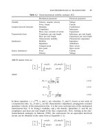
fref
x
f
sample
Figure
11.5
Block
diagram
of
dual
reference
and
sample
analogue
mixing
circuit
sensor
and
reference oscillators, producing some degree
of
baseline
offset.
Although
the
mixing
circuit technique will significantly reduce
the
effects
of
common mode interfer-
ence, there
is
always
the
possibility that interference could compound and, therefore,
increase measurement errors.
Another
option
is to use an
environmentally
isolated
precision
reference
oscillator.
As
the
frequency
from
this protected reference oscillator will remain
fixed, the
mixed
frequencies
from
the
reference
and
indicator sensor oscillator will
not
contain
frequency
contributions
from
any
interfering source (Crabb
and
Lewis 1973).
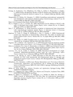
11.8
MEASUREMENT
SETUP
The
vector network analyser
and
associated calibration techniques make
it
possible
to
accurately
measure
the
transmission parameters
of the
devices under test.
The
measure-
ment
schematic
is
shown
in
Figure 11.6.
The
network analyser consists
of a
synthesized
sweeper
(10
MHz-40
GHz), test setup
(45
MHz-40
GHz), HP8510B network analyser,
and
a
display processor (Subramanian 1998; Piscotty
1998).
The
sweeper provides
the
stimulus
and the
test setup provides signal separation.
The
display panel
of the
HP8510B
is
used
to
define
and
conduct various measurements.
The
system
bus is
instrumental
in
controlling various other instruments.
The
device
to be
tested
is
connected between
the
test
Port
1 and
Port
2. The
point
at
which
the
device
is
connected
to the
test setup
is
called
the
reference
plane.
All
measurements
are
made with
respect
to
this reference
plane.
The
measurements
are
expressed
in
terms
of the
scattering parameters referred
to
as S
parameters (Subramanian 1998). These describe
the
signal
flow
within
the
network.
S
parameters
are
defined
as
ratios
and are
represented
by
S
inn
/
out,
where
the
subscripts
in
and
out
refer
to the
input
and
output
signal, respectively. Figure 11.7 shows
the
energy
flow
in
a
two-port network.
It can be
shown that (see
HP
8510B Network Analyser
Manual
1987)
b
1
=
a
1
S
11
=
a
2
S
12
and b
2
=
a
1
S
21
=
a
2
S
22
(11–2)
where
S
11
is
b\la\
and 5
21
is
b
2
la
1
when
a
2
is
zero;
5
12
is
b\la
2
and 522 is
b
2
/a
2
when
a\ is
zero.
S\\ and 5
21
(5i2
and
522)
are the
reflection
and
transmission
coefficients
for
Port
1(2), respectively.
344 IDT
MICROSENSOR
PARAMETER
MEASUREMENT
Synthesized
sweeper
0.01–40
GHz
HP
8510B
Network
analyzer
Test
set
0.045-40
GHz
Port
l
Coaxial
cable
Port
2
Power Macintosh
6100/66
HP
plotter
Apple
laser printer
Sample holder
with
SAW
device
T101
T101
Coaxial
cable
1 1
Figure 11.6 Schematic
of
measurement setup
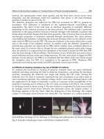
s
11
1
S
21
S
12
i
S
22
H
Figure 11.7 Signal
flow of a
two-port network
11.9 CALIBRATION
Calibration
of any
measurement
is
essential
in
order
to
ensure
the
accuracy
of the
system.
The
errors that exist
in
systems
may be
random
or
systematic. Systemic errors
are the
most
significant
source
of
measurement uncertainty.
These
errors
are
repeatable
and can
be
measured
by the
network
analyser.
Correction terms
can
then
be
computed
from
these
measurements. This
process
is
known
as
calibration. Random errors
are not
repeatable
and
are
caused
by
variations
due to
noise, temperature,
and
other environmental factors
that
surround
the
measurement system.
REFERENCES
345
A
series
of
known standards
are
connected
to the
system during calibration.
The
systemic
effects
are
determined
as the
difference between
the
measurand
and the
known
response
of the
standards. These errors
can be
mathematically related
by
solving
the
signal-flow
graph (Subramanian
1998).
The
frequency response
is the
vector
sum of all
test
setup variations
in
magnitude
and
phase
and the
frequency. This
is
inclusive
of all
signal-separation
devices,
such
as
test setup
and
cabling.
The
mathematical
process
of
removing
errors
is
called error correction. Ideally, using
perfectly
known standards, these errors should
be
completely characterised.
The
measure-
ment
system
is
calibrated using
the
full
two-port calibration method.
The
four
standards
that
are
commonly used
are
shielded open circuit, short circuit, load,
and
through. This
method provides
full
correction
of
directivity, source match, reflection
and
transmission-
signal
path, frequency response, load match,
and
isolation
for
S
11
, S
12
, S
21
,
and
S
22
.
The
procedure involves taking
a
reflection, transmission,
and
isolation measurement.
For the
reflection measurement (S
11
, S
22
),
the
open, short,
and
load standards
are
connected
to
each port
in
turn
and the
frequency response
is
measured. These
six
measure-
ments
result
in the
calculation
of the
reflection error coefficients
for
both ports.
For the
transmission measurement,
the two
ports
are
connected
and the
following
measurements
are
carried
out
forward through transmission
(S21
-frequency
response),
forward
through match
(S21-load),
reverse
through transmission (S
12
-frequency response),
and
reverse through match (S
12
-load).
The
transmission error
coefficients
are
computed
from
these
four
measurements.
Loads
are
connected
to the two
ports
and the S
12
and S
21
noise
floor
level
is
measured. From
these
measurements,
the
forward
and
reverse-isolation
error
coefficients
are
computed.
The
calibration
is
saved
in the
memory
of the
network analyser
and the
correction
is
turned
on to
correct systemic errors that
may
occur.
By
making these measurements,
it is
possible
to
identify
the
critical acoustic parameters
and
thus design
the
optimal IDT-SAW microsensor.
The SAW
microsensor
may now be
fabricated,
and the
process
is
provided
in the
following chapter.
REFERENCES
Avramov,
I. D.
(1989).
Analysis
and
design
aspects
of
SAW-delay-line-stabilised
oscillators,
Proceedings
of the 2nd
Int.
Conf.
on
Frequency
Synthesis
and
Control,
London,
April
10–13,
pp.
36-40.
Campbell,
C.
(1998).
Surface
Acoustic
Wave
Devices
and
their
Signal
Processing
Applications,
Academic
Press,
London.
Crabb,
J. and
Lewis,
M. F.
(1973).
"Surface
acoustic
wave
oscillators:
mode
selection
and
frequency
modulation,"
Electronics
Lett.,
9,
195–197.
Gangadharan,
S.
(1999).
Design,
development
and
fabrication
of a
conformal
Love
wave
ice
sensor,
MS
thesis,
Pennsylvania
State
University,
USA.
Grate,
J. W.,
Martin,
S. J. and
White,
R. M.
(1993).
"Acoustic
wave
microsensors,
Parts
I and
II,"
Anal.
Chem.,
65,
940–948, 987–996.
HP
8510B
Network
Analyzer
Manual
(1987).
Hewlett-Packard
Company,
Santa
Rosa,
Calif.
Piscotty,
D. J.
(1998).
150 MHz
wireless
detection
of a
ST-cut
quartz
substrate
surface
acoustic
wave
device,
MS
thesis,
Pennsylvania
State
University,
USA.
Shiokawa,
S. and
Moriizumi,
T.
(1988).
Design
of SAW
sensor
in
liquid,
Proc.
of 8th
Symp.
on
Ultrasonic
Electronics,
Tokyo,
July,
pp.
142–144.
346 IDT
MICROSENSOR PARAMETER MEASUREMENT
Smith,
W. R. and
Gerard,
H. M.
(1971). "Differences
between
in-line
and
cross-field
three-port
circuit
models
for
integrated
transducers,"
IEEE
Trans. Microw.
Theory
Techniques,
19,416-417.
Smith,
W. R. et al.
(1969).
"Analysis
of
interdigital surface wave
transducers
by use of an
equiv-
alent circuit
model,"
IEEE
Trans. Microw.
Theory
Techniques,
16,
856–864.
Subramanian,
H.
(1998).
Experimental validation
and
design
of
wireless
microaccelerometer,
MS
thesis, Pennsylvania
State
University, USA.
Wohltjen,
H. and
Dessy,
R.
(1979).
"Surface acoustic wave probe
for
chemical analysis," Anal.
Chem.,
51,471–477.
12.1 INTRODUCTION
Surface
acoustic wave (SAW) devices
are
fabricated using processes that have been
primarily developed
for
integrated circuit (1C) technology
in the
microelectronics
industry.
In
this chapter,
we
describe
all the
steps required
to
fabricate
an
interdigital trans-
ducer (IDT)
SAW
microsensor
from
a
stable temperature (ST)
cut
quartz wafer.
A
basic
overview
of
this process
is
given
in
Figure 12.1. Specifically, there
are two
processes that
are
commonly used
to
define
the
IDTs: etching
and
lift-off
(Hatzakis
et al.
1980). Both
methods
1
are
suitable
for the
fabrication
of
IDT-SAW delay-line sensors,
but the
ultimate
choice
of
either
the
etching
or the
lift-off
process
mainly
depends
on the
minimum feature
size (resolution
and
accuracy)
of the
patterned structure required. Although
the
etching
procedure
is
relatively easy
to
realise
and
acceptable resolution
is
achievable,
it is
more
susceptible
to
electrical shorts between features than that
of the
lift-off
process.
This
is a
major
concern, especially
for
minimum
feature
sizes approaching
1–2 um,
where
the
influ-
ence
of
contaminants, such
as
large dust particles, becomes more significant (Vellekoop
1994). However,
for
larger minimum feature sizes,
of 5 um or
greater,
it is
recognised
that
the
etching process
is
acceptable
and
comparable
in
terms
of
device fabrication yield
and
quality
to
that
of the
lift-off
process.
Section 12.2 provides
full
details
of the
steps required
to
make
an IDT
microsensor
through
either
an
etching
process
or a
lift-off
technique.
The
process
given here
is
meant
to
serve
as an
example,
and
variations
in the
precise choice
of
materials
and
equipment
used
will vary
from
laboratory
to
laboratory.
Next,
the
steps required
to
make
a
Rayleigh-SAW microsensor
from
the
IDTs
are
shown,
together
with
a
waveguiding layer
of
SiO
2
(Section 12.3)
to
fabricate
a
Love
wave
microsensor.
Finally,
in
Section 12.4,
we
provide tables that summarise
the
etching
and
lift-off
processes
and
present their relative merits.
12.2 SAW-IDT MICROSENSOR FABRICATION
12.2.1 Mask Generation
SAW-IDT
designs
are
written onto square, low-expansion glass plates using
a
process
of
electron-beam (E-beam) lithography.
The SAW
designs
are first
created using
a
1
Pattern
transfer
and
etching
methods
were
introduced
in
Chapter
2.
12
IDT Microsensor Fabrication
348 IDT
MICROSENSOR
FABRICATION
Figure
12.1
Overview
of
process
required
to
fabricate
Rayleigh
wave
and
Love
wave
IDT
microsensors
computer-aided
design
(CAD) system (e.g. L-Edit
from
Tanner
Tools
Inc.)
and
then
the
electronic
design
files are
exported
in a
standard format (e.g.
GDS II)
that
offers
compatibility with
the
E-beam writer.
The IDT
structures
are
thus written
on a
positive
resist material that coats
the
mask plate
on
which
a
thin chromium layer
has
already
been
deposited.
The
resist
is
developed
and the
chrome
is
etched away
to
leave
the
desired
IDT
structures.
It is
common practice
to
make
an
inverse mask,
or
negative,
from
the
master positive mask plates using
a
quicker
and
more inexpensive ultraviolet (UV)
optical lithographic
process.
It is
these copies that
are
then used
in the
silicon
run
and,
if
damaged,
can be
replaced immediately. Figure 12.2 shows
a
typical
IDT
design
that
would
be
written onto
the
positive
and
negative mask plates.
12.2.2
Wafer
Preparation
Effective
cleaning
of the
quartz wafers
is a
vital procedure, which
is an
essential require-
ment
for the
successful fabrication
of IDT
microsensors.
In
order
to
obtain
good
adhesion
and a
uniform
coating
of the
metallic
film
used
to
make
the
IDTs,
a
thorough cleaning
of
SAW-IDT
MICROSENSOR
FABRICATION
349
Figure
12.2
Basic
layout
of a
photolithographic
mask
plate
showing
an IDT
structure:
(a)
positive
and
(b)
negative
fields
the
wafer
surface
is
essential.
The
cleaning
of the
wafers should
be
performed
in a
fume
cupboard
(in a
clean room)
to
allow
the
safe
and
fast
removal
of any
possible
harmful
fumes
produced during
the
cleaning process (Campbell 1998; Atashbar 1999).
The
wafers
are
initially cleaned
of any
surface contaminants, such
as
dust, grease,
or any
other soluble organic particles,
by
immersion
in
trichloroethylene
2
at 60 °C for
10
minutes, followed
by an
acetone bath
at 60 °C for 10
minutes.
The
wafers
are
then
rinsed with methanol
and finally
with deionised water.
It is
best
to
avoid
the use of
nitrogen
gas for
drying
the
sample during
the
aforementioned procedure
so as to
minimise
further
surface contaminants. Instead,
a
slow evaporation
in a
protected
fume
cupboard
is
employed. Further cleaning
is
then undertaken
for the
removal
of the
more obstinate
contaminants.
The
wafers
are
immersed
in a
mixture
of
three parts
of
deionised water
(3H
2
O),
one
part ammonium hydroxide (NH
4
OH),
and one
part
of 30
percent unsta-
bilised hydrogen peroxide (H
2
O
2
)
at 75 °C for 10
minutes. Caution
is
required because
the
mixture
is
harmful,
and it is
recommended that
the
hydrogen peroxide
is
added last
so
as to
minimise
any
reaction side
effects.
Next,
the
wafers
are
placed
in a
solution
of
industrial grade detergent
and
subjected
to
ultrasonic agitation
at 60 °C for ten
minutes.
Following
a rinse in
deionised water,
the
wafers
are
placed
in a
circulating deionised
water
bath
for 30
minutes.
The
wafers
are
then dried using compressed
filtered
nitrogen
and
stored
in an
appropriate container
and
environment.
12.2.3
Metallisation
A
metal layer
now
needs
to be
deposited,
from
which
IDT
structures
are to be
formed.
In
general, aluminum
is
evaporated using,
for
example,
a
Kurt
Lesker™
E-beam evaporator.
Aluminum
is
employed because
it is
commonly used
in IC
foundries
and
exhibits chemical
resistance
to
many
different
liquids
3
.
Typically,
a 100 to 150 nm
layer
of
aluminum
is
deposited
on the
clean surface
of a
quartz wafer.
For
example,
the
beam voltage
of an
E-beam evaporator
is set to 6 keV
during
the
deposition
of 150 nm of
aluminum,
the
pre-evaporation pressure
is set at
10
-6
torr,
and the
beam current
is set to
almost
100 mA.
This gives
an
evaporation rate
of
0.2
nm/s.
It is to be
noted that aluminum could have also been evaporated onto
the
'
Caution
needs
to be
exercised since trichloroethylene
fumes
are
toxic.
3
Clearly,
strong
acids
attack
aluminum
and
should
be
avoided.
350
IDT
MICROSENSOR FABRICATION
device using thermal evaporation instead
of
using
the
E-beam technique.
The
E-beam
technique, however, allows more control over
the
deposition rate,
and the films
tend
to
be
more
uniform
and to
possess
fewer
stacking
faults
and
dislocations.
E-beam evaporation
of
aluminum
is,
indeed, compatible
with
both
the
etching
and the
lift-off
processes used later
on.
12.2.4 Photolithography
The
photolithography process
is
conducted
in a
clean room environment
at a
constant
temperature
of,
typically,
25 °C ± 1 °C and at a
relative humidity
of 40 ± 5
percent.
The IDT
structures need
to be
oriented correctly
with
respect
to the
quartz wafer
in
order
to
generate
the
required Rayleigh
(or
Love)
waves. Figure 12.3 shows
the
correct
orientation
of the
wafer
and the
SAW-IDTs
4
.
12.2.4.1
Etching process
The
etching
process
begins with
the
initial cleaning
of the
metallised
wafers, followed
by
the
deposition
of a
positive photoresist.
The
wafers
are first
rinsed
in a
bath
of
acetone
and
then
in
isopropanol
to
remove
any
possible
loose
surface contaminants that could have
appeared during storage since
the
initial wafer-cleaning procedure. Next,
the
wafer
is
thoroughly
rinsed
in a
deionised water bath
for 5
minutes, followed
by an
oven bake
at 75 °C for 20
minutes. This removes
any
moisture
from
the
surface
of the
wafer.
Using
a
Headway Research Inc.® spinner, hexamethyl disilazane (HMDS)
is
spun
on
the
wafer
at
3000
rpm for 60
seconds
to
improve
the
adhesion
of the
resist
to the
wafers.
After
allowing
the
HMDS thin
film to sit for 2
minutes,
AZ-1512®
positive photoresist
(Hoechst)
is
then spun
at
3000
rpm for 30
seconds.
A
photoresist layer, approximately
1.2 n,m
thick,
is
formed.
The
wafer
is
then baked
in an
oven
at 90 °C for 30
minutes
to
Major
flat
ST-quartz
Major flat
ST-quartz
Figure
12.3
Orientation
of an
ST-quartz
wafer
and the
SAW-IDT
structures
to
fabricate
Love
and
Rayleigh
wave
sensors
4
The
relationship
between
wafer
flats and
crystal
orientation
is
defined
in
Section 4.2.
SAW-IDT MICROSENSOR FABRICATION
351
remove
any
excess solvents
from
the
photoresist.
Then,
it is
cooled
to
room temperature
for
approximately
15
minutes before exposing
it to UV
light
in the
mask aligner.
A
contact mask aligner (Karl Suss MRK-3)
is
used
to
align
the
positive chrome mask
plate with
the
quartz that
is
wafer-coated with
the
photoresist.
A UV
light exposure
of
6
seconds
is
subsequently required.
The
exposed
wafer
is
then developed
in a
mixture
of
(ratio 1:4) AZ–450® developer (Hoechst)
and
deionised water
for 40
seconds. Great care
should
be
taken
at
this
stage
because under
or
overdeveloping
the
photoresist layer will
degrade
the
fabrication success.
It is
strongly recommended that
an
immersion style
is
adopted,
so
that
the
wafer
is
slowly agitated during
the
developing process
at 10
second
intervals, followed
by a
deionised water rinse
and a
close inspection using
a
microscope.
This will provide
for
greater
control
in the
important developing stage
of
fabrication.
A
'soft'
post bake
is
then performed
at 75 °C for 10
minutes, which assists
in the
hardening
and
formation
of
sharp features
of the
photoresist.
The
wafer
is
then allowed
to
cool
to
room
temperature
for
approximately
15
minutes.
At
this stage,
the IDT
pattern should
have
been successfully transferred
to the
wafer;
if
not,
the
photoresist
can be
stripped
off
in
acetone
and the
entire procedure repeated before
the
etching
of the
wafer.
Chemical wet-etching
of the
unwanted aluminum
is
then performed.
The
aluminum
layer
is first
etched
in a
solution
of a
commercial etchant
and
deionised water (3.25
g of
etchant
in 50 ml of
deionised water)
at
room temperature
for
approximately
60
seconds.
The
etching time
is
extremely critical because undercutting
of the
structure walls
may
occur
if
prolonged
times
are
employed.
It is
strongly
recommended
that etching
is
performed
at 10
second intervals, followed
by a
deionised water rinse
and
close inspection
with
a
microscope.
The
temperatures
of the
etchant solutions, together with
the
thickness
of the
metal
layers,
are
important factors that have
a
significant
influence
on the
etching times.
It is
recommended that
the
etching procedure
is
inspected
for
assurance before
the
processing
of
valuable quartz
wafers.
Once
the IDT
design
has
been successfully transferred
to the
metallised
wafer
via the
etching
process,
the
wafer
is
ready
for
dicing (Campbell 1996, 1998).
The
dicing process
is
described
briefly
in
Section 12.2.5.
12.2.4.2
Lift-off
process
The
lift-off
process begins with
an
initial cleaning
of the
wafers,
followed
by the
deposition
of
a
positive photoresist.
A
similar cleaning procedure
to
that used
for the
etching process
is
used
to
remove
any
possible
loose
surface contaminants that
may
have appeared during
storage since
the
initial wafer-cleaning procedure. Similarly, HMDS
is
spun
on to the
wafer
using,
for
example,
a
Headway Research
Inc.®
spinner
at
3000
rpm for 60
seconds
to
improve
the
adhesion
of the
resist
to the
wafer.
After
allowing
the
HMDS thin
film
to
sit for 2
minutes, AZ-1512®
positive
photoresist
(Hoechst)
is
then spun
at
3000
rpm
for
30
seconds.
A
photoresist layer
of
approximately
1.2 um is
formed.
The
wafers
are
then
baked
in an
oven
at 75 °C for 30
minutes
to
remove
any
excess solvents
from
the
photoresist.
The
wafers
are
cooled
to
room temperature
for
approximately
15
minutes
before
UV
light exposure.
After
aligning
the
negative
IDT
chrome mask plate with
the
photoresist-coated
wafer
having
a
similar orientation
to
that used
in the
etching process,
the
wafer
is
exposed
to
352 IDT
MICROSENSOR FABRICATION
UV
light
for 6
seconds.
To
improve
the
lift-off
capability,
the
wafer
is
then immersed
in
a
chlorobenzene bath
at
room temperature
for 3 to 3.5
minutes.
It is
important
to
note
that
this time varies depending
on the
intensity
of the UV
exposure lamp; typically,
for
an
intensity
of 21
W/cm
2
,
the
characteristic time
in
chlorobenzene ranges
from
about
220
to 280
seconds. This
is an
extremely critical step,
and the
procedure should
be
validated
before
it is
applied
to the set of SAW
wafers.
Chlorobenzene modifies
the
surface
of the
photoresist
by
developing
a
characteristic
'lip'
in the
developed
pattern.
This
creates
a
discontinuity
at the
edges
of the
patterned
photoresist when
a
metal
is
evaporated
on the
surface
of the
wafer; thus, unwanted metal
is
subsequently removed more
easily.
The
wafer
is
then baked
in an
oven
at 75 °C for
30
minutes
to
remove
any
excess solvents
from
the
photoresist
and
allowed
to
cool
to
room temperature
for
approximately
15
minutes.
The
wafer
is
then
developed
in a
mixture
(ratio 1:4)
of
AZ-450® developer (Hoechst)
and
deionised water
for 40
seconds.
Again, great care should
be
taken
at
this
stage,
as
under
or
overdeveloping
the
photore-
sist layer will degrade
the
fabrication success.
As in the
etching process,
an
immersion
method
is
strongly recommended, whereby
the
wafer
is
slowly agitated during
the
devel-
oping process
at 10
second intervals, followed
by a
deionised water
rinse and
then
close
inspection with
a
microscope.
It is
important
to
prevent damage
to the
photoresist-
patterned structures
at
this stage,
so
extremely gentle agitation
is
required
in the
immersion
step,
and the use of
compressed
filtered
nitrogen
for
drying
the
wafer
should
be
avoided.
Close inspection
of the
wafer
surface using
an
optical microscope
is
then performed
to
examine
the
transferred SAW-IDT pattern.
The
edges
of the
photoresist patterns should
be
well
defined
and
sharp
to
facilitate
the
lift-off
process. Again,
if
found
unacceptable,
the
photoresist
can be
removed using acetone
and the
entire procedure
can be
repeated
before
the
metallisation
of the
wafer.
After
the
metallisation
of the
photoresist-patterned
wafer
using
the
metal evaporation
technique (Section
12.2.4),
the
photoresist
is
removed
by
immersing
the
wafers
in an
acetone bath
at
room temperature
for 30
minutes. Ultrasonic agitation
may be
used
to
assist
in the
removal process
but
caution
is
advised
as
damage
to
small patterned structures
(feature
sizes
<2 nm) may
occur.
Once
the IDT
designs have been successfully transferred
to the
wafers
via the
lift-off
process,
the
wafers
are
then ready
for
dicing (Section 12.2.5).
A
summary
of the
photolithography
process
for
both
the
etching
and
lift-off
procedures
is
shown
in
Figure 12.4.
12.2.5 Wafer Dicing
The
wafers
are finally cut
into small, individual chips using,
for
example,
a
Deckel™
wire
saw, together with
a
diamond impregnated wire
and
slurry.
The
slurry
is
made
from
a
mixture
of
silicon, glycerol,
and
deionised water
(3:5:1)
and has a
particle
size
of 25 um.
Before
cutting
the
wafer,
a
thick layer
of
AZ-4562® positive photoresist (Hoechst)
is
spun
at
2000
rpm for 30
seconds,
following
the
deposition
of a
thin HMDS layer spun
on
to
improve
the
photoresist adherence
on the
wafer.
The
wafer
is
then baked
in an
oven
at
75 °C for 30
minutes
and
then allowed
to
cool
to
room temperature.
The
resulting thick
layer protects
the
delicately patterned
IDT
structures
during
the
debris
cutting.
DEPOSITION
OF
WAVEGUIDE
LAYER
353
Figure 12.4 Basic steps involved
in two
lithographic processes used
to
make
IDT
structure:
etching
(left)
and
lift-off
(right)
on a
piezoelectric (PE) substrate
12.3
DEPOSITION
OF
WAVEGUIDE LAYER
12.3.1 Introduction
Love wave sensors require
the
deposition
of a
guiding layer made
from
an
acoustic
material that
has a
shear wave velocity less than that
of the
quartz wafer. Described next
are the
process conditions
and
steps that should
be
followed
to
deposit SiO
2
as a
guiding
layer
on top of a
quartz wafer.
Steps that occur during
a
typical chemical deposition process include (Campbell 1996)
the
following:
1.
The
transport
of
precursors
from
the
chamber inlet
to the
proximity
of the
wafer
2.
Reaction
of
these gases
to
form
a
range
of
daughter molecules
3.
Transport
of
these
reactants
to the
surface
of the
wafer
4.
Surface reaction
to
release
the
SiO
2
5.
Desorption
of the
gaseous by-products
6.
Transport
of the
by-products away
from
the
surface
of the
wafer
7.
Transport
of the
by-products away
from
the
reactor
354 IDT
MICROSENSOR FABRICATION
12.3.2
TMS
PECVD
Process
and
Conditions
One of the
necessary conditions
for the
deposition
of
SiO
2
is
that
the
temperature
of
deposition should
be as low as
possible. This
is
desirable because higher temperatures
can
adversely
affect
the
poling characteristics
of
quartz
(in
spite
of the
fact
that quartz
is a
naturally piezoelectric material)
and
because
the
melting point
of the
metallisation
layer
(aluminum
is 650 °C)
should
not be
exceeded.
We
should therefore choose SiO
2
that
is
either sputtered
or
deposited
by
plasma-
enhanced chemical vapour deposition (PECVD)
from
silane
gas.
The
sputtering
process
provides better step-coverage than evaporation
and far
less radiation damage than
E-
beam evaporation (Campbell 1996).
A
simple sputtering system consists
of a
parallel-plate
plasma
reactor
in a
vacuum chamber
and the
target material (SiO
2
) placed
on the
electrode
such that
it
receives
the
maximum
ion flux. An
inert
gas (at a
pressure
of 0.1
torr)
is
usually
used
to
supply
the
chamber with high-energy ions that strike
the
target
at
high velocities
and
dislodge
the
SiO
2
molecules, which deposit conformal
to the
wafer
(the SAW-IDT
device).
The
only disadvantage
in
this process
is
that
on
account
of the
physical
nature
of
the
process,
sputtering could
also
bombard
and
damage
the
delicate
IDT fingers on the
surface
of the
quartz. Sputtering
can
also introduce
a
variety
of
contaminants
from
the
substrate
holder because
of the
physical nature
of the
process. Hence, sputtering
is not
the
ideal means
of
depositing SiO
2
, despite
the
fact
that
the
process
can be
carried
out
under
conditions
of low
temperature.
An
alternative approach
is to use
chemical vapour deposition (CVD).
A
simple
CVD
process
is
shown
in
Figure 12.5.
The
reactor consists
of a
tube with
a
rectangular cross
section,
and the
walls
of the
tube
are
maintained
at a
temperature
T
w
. A
single
wafer
rests
on
a
heated susceptor
in the
centre
of the
tube.
This susceptor
is
maintained
at a
temperature
T
s
(where
T
s
T
w
).
The
obvious choice
is
to use
oxidised silane
gas
(SiH
4
) (also referred
to as
tetraethoxysilane TEOS)
to
form
SiO
2
in the
presence
of an
oxidising agent, such
as O2, and an
inert
carrier
gas, such
as
H2
(to
improve
the
uniformity
of
deposition). Excessive homogeneous reactions occurring
spontaneously
in the gas
above
the
wafer
will
result
in the
deposition
of
large
Si
particles
in
the gas
phase,
and
their subsequent deposition
on the
wafer
will
cause poor
surface
morphology
and
inconsistent
film
properties.
Figure
12.5
A
simple
CVD
process
flow
system
DEPOSITION
OF
WAVEGUIDE
LAYER
355
Some
of the
other problems associated with PECVD (TEOS)
are
that
(7)
quality
plasma-enhanced chemical vapour-deposited tetraethoxysilane (PETEOS) SiO
2
films are
difficult
to
achieve
at
temperatures below
250 °C
(Alaonso
et al.
1992; Itani
and
Fukuyama
1997)
and (2)
TEOS
has a low
vapour pressure
of
approximately
2
mTorr
(25 °C and
1
atm), which necessitates
the
heating
of all
delivery lines
and
chamber
surfaces
to
prevent
TEOS condensation
and
prevents
gas
metering with conventional mass-flow
controllers,
thus
rendering
the
resulting process prohibitively expensive (Ballantine
et al.
1997).
Conventional mass-flow controllers,
on the
other hand, easily meter silane gas,
but
great care must
be
used because silane
is a
toxic
and
pyrophoric
gas and
constitutes
an
explosion hazard
at
high
SiFU
concentrations. These limitations
add to the
cost
and
complexity
of
TEOS
and
silane-based silicon deposition equipment.
To
achieve
a low
temperature, good quality oxide,
and for the
circumvention
of the
safety
issues associ-
ated with silane-based oxides
and the
manufacturing complexities inherent with TEOS,
an
alternative precursor needs
to be
employed.
Potential organo-silicon precursors
are
compiled
and
their critical physical
and
chemical
properties
are
tabulated
for
comparison with
the
properties
of
silane
and
TEOS.
Of all
the
precursors
listed
in
Table 12.1, tetramethylsilane (TMS)
can be
chosen
as the
best
precursor
for the
current low-temperature application
for
several reasons.
TMS is
known
to be
nontoxic
and
nonpyrophoric,
and its
high vapour pressure
(580 mTorr) allows
for the use of
conventional
mass-flow
controllers
at
room temperature.
Table 12.1 Tabulation
of
relevant parameters
for
feasible PECVD precursors (Gangadharan
1999)
Precursor
Chemical
Name
Formula
MW
State
@
20 °C
Best
Assay
VP@20°C
(mTorr)
Use
stand.
MFC
Stability
Flammable
Pyrophoric
Toxicity
(ppm)
**
Values
not
Silane
Silane
SiH
4
32
Gas
**
Gas
Yes
Unstable
Yes
Yes
Toxic
(0.5)
known.
TEOS
Tetraethoxy
silane
Si(C
2
H
5
O)
4
208.3
Liquid
>99.99
1.5
No
Stable
Yes
No
Nontoxic
(100)
TMS
Tetramethyl
silane
Si(CH
3
)
4
88.2
Liquid
99.90
589
Yes
Stable
Yes
MS
Methyl
silane
CH
3
SiH
3
46
Gas
Yes
**
Yes
**
**
TMCTS
1,3,5,7 Tetra
methylcyclo
tetrasiloxane
C
4
H
16
0
4
Si
4
240.5
Liquid
99.90
6
Not
sure
**
Yes
Not
sure
**
LTO-410,
DBS
Diethyl-
silane
SiH
2
(C
2
H
5
)
2
88.2
Liquid
>
99.70
207
Yes
Stable
Yes
**
**
356 IDT
MICROSENSOR FABRICATION
Also, each parent
TMS
molecule (Si(CH3)
4
) contains half
as
much carbon
and
three-
fifths as
much hydrogen
as a
TEOS molecule (Si(OC2H
5
)4),
and it is
hypothesised
that
carbon
and
hydrogen-free
films
will
be
obtainable
at
lower temperatures
from
this
precursor. Additionally,
the
lower molecular weight
of TMS
might allow
for
higher surface
mobility than TEOS
at any
given temperature, thereby resulting
in
better-quality
films at
temperatures lower than those obtainable
by
PETEOS
(~250
°C). Finally,
it is
thought that
PECVD
TMS
oxide (PETMS-O
x
) deposition conditions could mimic very closely those
conditions
found
to
produce high-quality PETEOS
and
silane oxides
in the
semiconductor
industry
(Campbell 1996; Ghandi 1994). Such deposition
is
carried
out
using
a
cluster
tool that
is
specifically fabricated
for
this
process,
and the
four-chamber showerhead
Vactronics
PDS-5000
S
cluster tool PECVD reactor (Figure 12.6)
is
used.
The
deposition procedures
and
conditions involve
units
3 and 4 as
follows: initially,
in
the
deposition chambers, TMS,
02, and He gas
lines
are
evacuated
of
residual
gas
and
then
a
sample
is
placed
in a
load-lock chamber
(unit
3),
which
is
evacuated
from
atmosphere
to a low
pressure (typically
10
—5
-10
—6
torr). This preinsertion
vacuum
time
is
held
at 30
minutes.
The
SAW-IDT
wafer
is
then placed
on the
preheated sample stage
(unit
4) in the
deposition chamber, which
is
maintained
at
10
—6
to
10
—7
torr,
by the
robotic loading mechanism.
A
period
of 1
hour
is
allotted
for the
sample
to
come
to
temperature,
after
which
02 and He
gases
are
input
via the
gas-dispersion showerhead
and
a
period
of 5
minutes
is
allotted
for the flows to
stabilise.
A
plasma
is
struck
with
the
same pressure,
RF
power,
and gas flow
rates. This
10-minute
preclean plasma
purge
serves three purposes:
1.
It
removes
any
residual carbonaceous matter
left
on the SAW
device
2. It
helps
to
form
a
stable interface oxide
3.
It
provides
a
high
flow,
stable
plasma into which
a
miniscule
flow of TMS can be
injected
Figure
12.6
Schematic
representation
of a
PECVD
unit
DEPOSITION
OF
WAVEGUIDE
LAYER
357
Table
12.2
Main
steps
involved
in the
etching process
Step Description
(a)
Exposure
of
photoresist metallised wafer with positive
IDT
mask plate.
(b)
Develop photoresist patterned structures.
(c)
Removal
of
unwanted metallisation layer
via
chemical wet-etching.
(d)
Removal
of
photoresist layer.
Table
12.3
Main steps involved
in the
lift-off
process
Step Description
(a)
Exposure
of
photoresist bare
wafer
with negative
IDT
mask plate.
(b)
Develop photoresist
and
formation
of the
characteristic
lip.
(c)
Deposition
of
metal layer onto
the
wafer.
(d)
Removal
of
unwanted metallisation
via
acetone rinse.
Table
12.4
Summary
of the
main advantages
and
disadvantages
of the
etching
and
lift-off
proce-
dures
Etching
procedure
Advantages: Disadvantages:
Simple
and
reproducible
Process
parameters must
be
characterised
Good resolution achievable Compatibility
of
chemical etchants with
substrates
Fast realisation Loss
of
feature resolution
due to
overetching,
tendency
to
undercut
Ideal
for
small batch processing Susceptible
to
electrical shorts
Lift-
off
procedu
re
Advantages:
Disadvantages:
Capable
of
higher resolution Extreme
care
in
handling before metallisation
Occurrence
of
electrical shorts minimised Intimate-contact photolithography required
to
achieve vertical sidewalls
on
patterned
photoresist structures
Photolithography process
is
independent
of
pattern resolution
Etchants
not
required Poor 'lift-off possible because
of
incorrect
formation
of
characteristic
'lip'
Ability
to
reprocess patterned photoresist
structures
before metal layer deposition
At
the end of
this preclean,
the
plasma remains
and TMS
vapour
is
introduced.
It is
metered using
a
conventional
10
cubic centimeter
per
second (cc/s) mass-flow controller
(MFC)
to the
desired volumetric
flow
rate.
The
oxide deposition begins
at
this point
and
is
continued
for a
predetermined time
to
achieve
an
oxide
film of the
desired thickness.
Following
the
deposition,
the TMS gas is
turned off,
but the
O
2
-He
plasma
is
kept
on
358 IDT
MICROSENSOR
FABRICATION
for
postdeposition
cleaning.
Once
the 15
minute
postdeposition
cleaning
is
completed,
the
plasma
is
extinguished,
the
gases
are
turned
off,
and the
chamber
is
evacuated
for
3
minutes.
Finally,
a
robotic
transporter
can
shuttle
the
SAW-IDT
wafers
to the
load-lock
chamber
(unit
3),
where
they
are
subsequently
removed.
12.4
CONCLUDING
REMARKS
This
chapter
has
described
in
detail
two
process
runs
that
can be
followed
to
fabricate
a
Rayleigh
wave
IDT
microsensor
or a
Love
wave
IDT
microsensor
(Gangadharan
1999).
The
main
steps
for the
etching
process
are
given
in
Table
12.2
and for the
lift-off
process
in
Table
12.3.
These
tables
provide
the
reader
with
a
list
of the key
steps
of the
two
processes
described
in
Section
12.2.4
earlier.
A
summary
of the
main
advantages
and
disadvantages
of the
etching
and
lift-off
processes
is
given
in
Table
12.4.
They
are
relevant
to the
fabrication
of
SAW-IDT
microsensors
and are
taken
from
a
number
of
sources
(Campbell
1996, 1998;
Atashbar
1999).
The
next
chapter
describes
the use of
SAW-IDT
devices
in a
number
of
different
sensing
applications.
REFERENCES
Alaonso,
J. C,
Ortiz,
A. and
Falcony,
C.
(1992).
"Low temperature SiO
2
films
deposited
by
plasma
enhanced techniques," Vacuum,
43,
843-847.
Atashbar,
M. Z.
(1999).
Development
and
fabrication
of
surface acoustic wave (SAW) oxygen
sensors
based
on
nanosized TiO
2
thin
film, PhD
Thesis,
RMIT, Australia.
Ballantine,
D. S. et al.
(1997).
Acoustic
Wave
Sensors:
Theory,
Design
and
Physico-Chemical Appli-
cations,
Academic
Press,
London.
Campbell, A.S.
(1996).
The
Science
and
Engineering
of
Microelectronic Fabrication, Oxford Uni-
versity
Press,
Oxford, England.
Campbell,
C.
(1998).
Surface
Acoustic
Wave
Devices
and
their Signal Processing Applications,
Academic
Press,
New
York.
Gangadharan,
S.
(1999).
Design, development
and
fabrication
of a
conformal Love wave
ice
sensor,
MS
thesis (advisor
V. J.
Varadan), Pennsylvania State University, USA.
Ghandi,
S. K.
(1994).
VLSI
Fabrication Principles: Silicon
and
Gallium Arsenide, John Wiley
and
Sons,
New
York.
Hatzakis,
M.,
Canavello,
B. J. and
Shaw,
J. M.
(1980). "Single-step optical
lift-off
process,"
IBM
J.
Res. Develop.,
24,
452-460.
Itani,
T. and
Fukuyama,
F.
(1997).
"Low temperature synthesis
of
plasma
TEOS
SiO
2
,"
Mat. Res.
Soc. Symp., 446,
p.
255.
Vellekoop,
M. J.
(1994).
A
smart Lamb-wave sensor system
for the
determination
of fluid
proper-
ties,
PhD
Thesis,
Delft
University,
The
Netherlands.
13
IDT
Microsensors
13.1
INTRODUCTION
Surface
acoustic wave (SAW) devices
possess
several properties such
as
high reliability,
crystal stability, good reproducibility,
and
relatively small size that make them suitable
for
many sensing applications. They
can be
used
to
sense many
different
properties,
for
example, strain, stress, force, pressure, temperature,
gas
concentration,
electric
voltage,
and
so
forth.
Readers
are
referred
to a
recent article
by
Hoummady
et al.
(1997)
for a
review
of
their applications.
One
attractive feature
of
some types
of SAW
sensor
is
that they
can be
read remotely.
The
operating
frequency
of a SAW
device typically ranges
from
10 MHz to a few
GHz,
which
corresponds
to the
operating
frequency
range
of
radio
and
radar communication
systems,
respectively.
Thus, when
an
interdigital transducer (IDT)
sensor
is
directly
connected
to an
antenna,
the
electromagnetic waves received
by
wireless transmission
can
excite
SAW in the
piezoelectric material.
The
fundamentals
of
both
SAW
devices
and
acoustic waves
in
solids
were
considered
in
Chapters
9 and 10, and it was
evident
that
passive, wireless
(or
remotely operable)
SAW
devices
can be
made.
The
latter
is an
attractive
proposition when low-power sensors
are
needed
and are
even more attractive
for
use in
remote, inaccessible locations,
for
example, when buried
in
concrete
or in the
ground.
Wireless SAW-based microsensors
are
described
in
detail
in
Section 13.3.
The
sensing mechanism
of
SAW-
IDT
microsensors
is
based
on a
change
in the
prop-
erties
of the SAW
(e.g. amplitude, phase,
frequency,
or
velocity) when
the
measurand
changes. Basic
descriptions
of the
acoustic parameters that
can be
used
in a
generalised
measurement system have been given
in
Chapter
11.
In
this chapter,
we
present
a
number
of
different
applications
of SAW
microsensors
together with
the
equations that govern their behaviour.
For
example,
in
chemical
sensors,
the
SAW
couple into
a
thin chemically sensitive coating
and its
properties perturb
the
nature
of the
waves. Several
different
properties
of the film
coatings
can
affect
the
acoustic
waves,
namely, mass, density, conductivity, electrical permittivity, strain,
and
viscoelas-
ticity.
In
general,
the
change
in
acoustic velocity
u
a
can be
related
by the
total
differential
theorem
to the
change
in any
property
or
properties.
The
following equation applies
for
changes
in
mass, electrical, mechanical,
and
environmental parameters (Hoummady
et al.
1997).
(13.1)
c
"elec
"mech
360
IDT
MICROSENSORS
Because
the
change
in
acoustic velocity
of a SAW
microsensor
is a
combination
of
these
different
parameters, care
must
be
taken
in the
choice
of IDT
design
and
signal processing
techniques
so
that only changes
in the
desired parameter,
such
as
mass,
are
measured
and
not
the
cross-interfering signals
from,
for
example, mechanical strain
or
environmental
temperature.
The
coupled-mode theory
of SAW
devices helps
us to
understand
the
nature
of
these types
of
microsensors.
13.2
SAW
DEVICE MODELING
VIA
COUPLED-MODE
THEORY
The use of
coupled-mode theory
on SAW
devices
for
different
geometric
designs
and
choice
of
piezoelectric material
is
clearly described
by
Pierce (1954)
and
Campbell
(1998).
The
benefit
of
this approach
is
that
a SAW
device
can be
represented
by a set of
transfer
matrices
corresponding
to its
basic elements.
There
are
generally three elements
of a SAW
device: IDT, spacing,
and
reflector.
These
can
be
described
by the
transfer matrices
of T, D, and G,
respectively.
T
matrix
is a 3 x 3
matrix,
whereas
D and G are 2 x 2
matrices.
The T
matrix describes
the IDT
input
and
output
of
SAWs
as
well
as the
electromechanical conversion between
the
electrical
signal
and
the
SAW. Thus,
the T
matrix
has
three ports
of
which
two are
acoustical ports
and one
is an
electrical
port.
The
transfer matrix
D
describes
a SAW
propagation path between
two
representative sections, while matrix
G
represents
a
reflector array. Detailed mathematical
forms
of
these transfer matrices
are
given
in
Appendix
J.
Depending
on the
precise
configuration
of a SAW
device,
any
number
of T, D, and
G
matrices
can be
used,
but
their
basic
forms
remain
the
same.
For
example,
a SAW
microsensor comprising
an IDT and a
reflector (Figure 13.1)
can be
modeled
simply
by
using
three
transfer
matrices
TI, D2, and G
3
, as
illustrated
in
Figure 13.2.
Figure
13.1
Basic
elements
of a
SAW-IDT
microsensor:
IDT
(left), spacing
and
reflector (right)
Figure
13.2 Schematic representation
of a SAW
device
using
transfer matrix elements
SAW
DEVICE
MODELING
VIA
COUPLED-MODE
THEORY
361
Figure 13.1 shows
the
actual device layout that
has a
metallic IDT, metallic reflector,
and
spacing
in
between
on top of a
piezoelectric
substrate
1
. Thus, they
can be
represented,
as
shown
in
Figure 13.2, with transfer matrices
T, D, and G for
each element
of the SAW
device (the numbers
1, 2, and 3 are
shown
for
bookkeeping purposes when dual devices
or
even array devices
are
modeled).
The
electrical signals passing
in and out of the IDT are
represented
by the
scalars
a
and
h. The
SAWs coming
in and out of
each representative element
are
described
by the
symbols
+
W and ~W - one for
each propagation direction. Thus,
any (n —
l)th
SAW
amplitude
coming
in and out of the nth
section
(T, D, or G) has the
following relation,
where
the
components
of the
transfer matrices
are
represented
by
italic typeface.
(13.2)
This matrix representation
of a
lumped system model
of a SAW
device
allows other
SAW
structures
to be
modeled
as
well.
As
long
as the SAW
device
is a
combination
of
IDT, reflectors,
and
spacings, corresponding transfer matrices
can be
used
in the
same
order
as the
actual device layout. Figures 13.3
and
13.4 show
the
structures
and
models
of an
IDT-IDT
pair
and a
two-port
SAW
resonator. More complex structures
of
SAW
devices
can
also
be
modeled
by
just adding more transfer matrices
at
appropriate
locations.
The
acoustic part
and the
electrical part
of the
signals
W
i
can be
conveniently sepa-
rated
for the IDT
equations
and
hence solved
to
determine
the SAW
amplitudes. Then,
the
overall acoustic part
can be
represented
by the
simple product
of
each acoustic
transfer
matrix
in
turn.
For
example,
the
overall acoustic matrix
for the
resonator shown
W,
"3
U
3
it
Figure 13.3 Schematic representation
of an
IDT-IDT
pair
and its
transfer matrix model
1
Fabrication details
of IDT
microsensors
are
given
in
Chapter
12.
362 IDT
MICROSENSORS
+
W
-
W
G
D T D T D G
Figure
13.4
Schematic representation
of a
two-port
SAW
resonator
and its
transfer matrix model
in
Figure 13.4
may be
described
by
=
[G,]-[D
2
]
[D
4
]
•
[T
5
]
•
[D
6
]
•
[G
7
]
(13.3)
where
[T3]
and
[75]
are 2 x 2
acoustic submatrices
of a 3 x 3 T
matrix,
and an
overall
acoustic matrix
[M] (or M) can be
defined
as
[M]
=
[G
1
]
•
[D
2
]
•
[T
3
]
•
[D
4
]
• T
5
•
[D
6
]
•
[G
7
]
(13.4)
Likewise,
the
acoustic part
of
other
SAW
devices
can
also
be
modeled
in a
straightforward
manner.
The SAW
amplitudes associated with
an IDT
have
an
electrical part
as an
input
or
output
power.
For
example,
from
Figure
13.4,
(13.5)
where
03 is the
scalar input power
to IDT 3 and
[t3]
is a 2 x 1
submatrix
of the 3 x 3 T
matrix.
Knowing
that
r_LMA,i
r.uu/^1
(13.6)
and
(13.7)
SAW
DEVICE
MODELING
VIA
COUPLED-MODE
THEORY
363
substituting Equations
(13.6)
and
(13.7)
into Equation (13.5) gives
an
overall
transfer
matrix
of the SAW
device
in
terms
of
W0'S
and
W7's
for a
given
input
#3, as
shown
in
the
following equation:
[M]
a
3
-[Gi]-[D
2
]'[T
3
]
(13.8)
By
applying
the
appropriate boundary conditions, Equation (13.8) becomes soluble with
two
subequations
and two
unknown parameters. Usually,
the
boundary conditions
are
W
0
= 0 and
—
W
7
= 0
because there
are no
external sources
to
SAWs, that
is,
from
outside
the
device.
Any
reflections
of the
SAWs
from
the
substrate edges,
or
other struc-
tures
outside
the SAW
device,
are
suppressed
by
using
an
acoustic absorber and/or serrated
(or
slanted) edges.
The
basic
form
of the
transfer matrices remains
the
same
for
other devices, whereas
some
of the
parameters inside
the
transfer matrix
are
changed according
to the
choice
of
material
and
geometric constants.
For
example,
a SAW
gyroscope
is a
combination
of a
SAW
resonator (Figure 13.4)
and a SAW
sensor (Figure 13.1) placed orthogonal
to
each
other,
as
shown
in
Figure 13.5.
By
providing
a
known power
to an IDT of the
resonator,
the
response
of the
resonator
part
can be
solved
in
just
the
same
way as
before.
The
only difference
in
solving
the
sensor part
is the
boundary condition
on
each
IDT
because secondary waves
are
generated
upon
device rotation
and
they become
an
input
SAW to the
passive
IDT
that acts
as a
Coriolis
sensing element.
The
secondary SAWs
are +W
2
and —W
1
and +Wo and
—
W
3
and
are
again zero, provided there
are no
external
SAW
sources. Outputs
b\ and b
3
are the
resultant
electrical
signals because
of the
secondary
SAW
(Figure
13.6).
Again,
different
SAW
devices
can be
modeled
in
similar ways
and
solved
by
applying
the
appropriate
boundary
conditions.
m
Figure
13.5
Basic
layout
of a
SAW-IDT
gyroscope:
a
pair
of
IDTs
and a SAW
resonator
364
IDT
MICROSENSORS
w
i t
Figure
13.6
Model
of a SAW
sensor
with
secondary
SAW as
boundary
conditions
13.3
WIRELESS
SAW-BASED
MICROSENSORS
In
order
to
obtain
a
high sensitivity,
SAW
microsensors
are
usually
constructed
as
electric
oscillators
2
using
the SAW
device
as the
frequency control component.
By
accurately
measuring
the
oscillation
frequency,
a
small change
in the
physical variables
can
be
detected
by the
sensors.
A
typical
SAW
oscillator sensor schematic
is
shown
in
Figure 13.7.
Briefly,
an
amplifier
connects
two
DDTs
on a
piezoelectric
wafer
so
that oscillations
of
the SAW
propagating
from
one IDT to the
other
are set up by
feedback.
The
oscillation
frequency
satisfies
the
condition that
the
total phase
shift
of the
loop equals
2n and
varies with
the SAW
velocity
or the
distance (spacing) between
the
IDTs.
The
oscillator
includes
an
amplifier
and so
requires
an
external electrical power supply and, therefore,
cannot
be
operated
in a
passive wireless mode.
As
stated
earlier,
the
operating frequency
of SAW
devices ranges
from
10 MHz to a
few
GHz. When
an IDT is
directly connected
to an
antenna,
the SAW can be
excited
remotely
by
electromagnetic waves. Thus,
it is
possible
to
construct passive, wireless,
remotely
operable
SAW
devices.
The
applications
of
remote sensors
was first
reported
by
Bao et al.
(1987).
The
temperature
of a
passive
SAW
device
with
a
small
antenna
can be
remotely read
out by a
microwave communications system (Suh
et al.
2000).
2
Acoustic
wave
oscillators
are
described
in
Section
11.7.
WIRELESS
SAW-BASED MICROSENSORS
365
Amplifier
Frequency
counter
IDT
IDT
Figure
13.7
Schematic
diagram
of an
oscillator
SAW
sensor
with
a SAW
resonator
Device
antenna
Reflectors
IDT
Figure
13.8
Schematic
diagram
of a
remote
reading
sensor
system
with
passive
SAW
sensor
The
schematic diagram
of IDT and
reflectors
in
Figure 13.8 shows
the
basic operating
principle
of an IDT
with
a
wireless communication interface.
One IDT and two
reflectors
are
fabricated
on the
surface
of a
piezoelectric crystal
wafer.
These micro
IDT and SAW
sensors
can be
fabricated using
the
microlithographic process described
in the
previous
chapter.
The IDT
connects directly
to a
small antenna called
the
device antenna. This antenna-
IDT
configuration
is
able
to
convert
the
microwave signal
from
air to SAW
signal
on
the
wafer surface
and
vice
versa.
The
reading system
has a
linear
frequency-modulated
(FM) signal generator with
a
system antenna that transmits these
FM
signals.
The
signals
are
then received
by the
device antenna
and
converted
by the
antenna-IDT
to
SAWs
that
propagate along
the
surface
of the
piezoelectric
wafer.
366
IDT
MICROSENSORS
The
echoes
from
the two
reflectors
are
picked
up by the
antenna-IDT
and
sent back
to
the
system antenna.
The
echo
signals
are
delayed
copies
of the
transmitted
FM
signal.
The
delay times mainly depend
on the
velocity
of the SAW and the
distance between
the IDT
and
the
reflectors.
A
mixer, which takes
the
transmitted
FM as a
reference signal, outputs
the
signals
of
frequency difference between
the
reflected
and the
transmitted signals.
Because
the
transmitted signal
is
linearly
FM, the
frequency difference
is
proportional
to
the
time delay.
By
using
a
spectrum analysis technique, such
as a
fast
fourier transform
(FFT),
the two
echo signals
can be
separated
in the
frequency
domain because
the
delay
times
are
different.
Figure 13.9 shows
the
layout
of a
transceiver telemetry system
developed
by a
small
US
company (HVS Technologies).
This
system
operates
in the
range
of 905 to 925
MHz.
The
circuit
operates
as
follows:
The
input signal
is
pulsed
FM. A
pulser synchronises
the
direct current (DC) voltage
ramp circuit, voltage
controlled
oscillator
(VCO) output,
and the A/D
converter during
pulses
of
typically
16 ms
duration. During
the
pulse,
the DC
voltage ramp circuit linearly
tunes
the VCO
from
905 to 925
MHz.
The VCO
output
is
controlled
by a
diode
switch
and
then amplified
to 50 mW by a
high isolation amplifier.
A
coupler diverts
a
sample
of
the
signal
to the LO
input
of the
mixer.
A
circulator sends
the
transmitted signal
to
the
antenna
and
also
the
reflected signal, through
an
automatic gain control
amplifier,
to
the
radio
frequency
(RF)
input
of the
mixer. Then,
a
low-pass
filter
removes
any
high-
frequency
noise
and
signals
and
then
the
signal
is
digitised
at 10 M
samples
per
second
at
10 bit
resolution. Finally,
a
programmable digital signal processing (DSP) chip, such
as the TI
TMS320C3X,
is
used
to
extract
the
delay information
and
compute
the
desired
parameter. This value
is
then shown
on a
liquid
crystal display (LCD).
DSP/FFT
i
Output
LCD
Figure
13.9 System
for
remote sensing application
APPLICATIONS
367
13.4 APPLICATIONS
In
this section,
we
present
in
detail some examples
of the
applications
of
SAW-IDT
devices
as
temperature, strain, pressure, torque, rotation rate (gyroscope), humidity,
and
so
forth
sensors.
In the
next chapter,
the
applications
are
extended
to
include micro-
electromechanical system (MEMS)
IDT
structures along with IDTs
for
remote sensing
of
acceleration.
13.4.1 Strain Sensor
In
this section,
a
remote MEMS-IDT strain sensor system
is
employed
to
study
the
deflection
and
strain
of a
'flex-beam' type structure
of a
helicopter rotor (Varadan
et al.
(1997)).
The
system
is
based
on the
fact
that
the
phase delay
is
changed because
of the
strain
in the
sensor substrate.
The
system consists
of a
remote passive
SAW
sensor read
by
a fixed
microwave system station.
The FM
signal sent
by the
system antenna
is
expressed
as
S(t)
= A
COS(O)Q
+
fit/2)t (13.9)
where
COQ
is the
initial
frequency
of the FM
signal,
/JL
is 2n
times
the
rate
of
modulation,
and
t is
time.
The
echoes
from
the two
reflectors,
S\(t}
and
82(1),
are the
same
as the
transmitted
signal
S(t)
but
with
different
amplitudes
and
time delays
t\ and t
2
,
respectively. These
may
be
written
as
Si(0
= A
1
cos(w
0
+
V>t/2)(t
-
fi)
(13.10)
and
S
2
(t)
=
A
2
cos(o)
0
+
l^t/2)(t
-t
2
)
(13.11)
with
+ T
e
(13.12)
+ r
e
(13.13)
where
v is the SAW
velocity,
d\ and d
2
are the
distances
from
the IDT
transducer
to
the
two
reflectors,
and r
e
is the
total
of
other delays (such
as the
delay
in the
electronic
circuit
and
devices
and the
traveling time
of the
electromagnetic wave
3
) that
is the
same
for
both echoes.
Through
the
mixer that uses
the
transmitted signal
as a
reference
and
low-pass
filter,
frequency
differential
signals
are
obtained
as
Ei(t)
= BI
COS\JJLtit
+
(cOQti
-
fJLti)]
= BI
COS[(i>it
+
<pi]
(13.14)
and
E
2
(t)
= B
2
cos[/Ltf
2
f
+
(co
0
t
2
- nt] = B
2
cos[co
2
t
+
(p
2
]
(13.15)
3
For
short
distances,
this
time
is
negligible.