Encycopedia of Materials Characterization (surfaces_ interfaces_ thin films) - C. Brundle_ et al._ (BH_ 1992) WW Part 6 ppsx
Bạn đang xem bản rút gọn của tài liệu. Xem và tải ngay bản đầy đủ của tài liệu tại đây (1.5 MB, 60 trang )
The strengths of
XPS
are its good quantification, its excellent chemical state
determination capabilities, its applicability to a wide variety of materials
from
bio-
logical materials to metals, and its generally nondestructive nature.
XPS's
weak-
nesses are its lack of good spatial resolution
(70
p),
only moderate absolute
sensitivity (typically 0.1 at.
%),
and its inability to detect hydrogen. Commercial
XPS
instruments are usually fully
UW
compatible and equipped with accessories,
including a sputter profile gun. Costs vary from
$250,000
to
$600,000,
or
higher if
other major techniques are included.
UPS
differs from
XPS
only in that it uses lower energy radiation to eject photo-
electrons, typically the
2
1.2-eV and 40.8-eV radiation from a He discharge lamp,
or
up to 200 eV at synchrotron facilities. The usual way to perform
UPS
is to add a
He lamp to an existing
XPS
system, at about an incremental cost of
$30,000.
Most
activity using
UPS
is in the detailed study of valence levels for electronic structure
information.
For
materials analysis it is primarily
useful
as
an adjunct to
XPS
to
look at the low-lying core levels that can be accessed by the lower energy
UPS
radi-
ation sources. There are several advantages in doing this: a greater surfice sensitivity
because the electron kinetic energies are lower, better energy resolution because the
source
has a narrower line width, and the possibility of improved lateral resolution
using synchrotron sources.
Auger Electron Spectroscopy,
AES,
is also closely related to
XPS.
The hole left in
a core level after the
XPS
process, is filled by an electron dropping fiom a less tightly
bound level. The energy released can be used to eject another electron, the Auger
electron, whose energy depends only on the energy levels involved and not on
whatever made the initial core hole. This allows electrons, rather than
X
rays, to be
used to create
the
initial core hole, unlike
XPS.
Since
all
the energy levels involved
are either core or valence levels, however, the type of information supplied, like
XPS,
is elemental identification from peak positions and chemical state informa-
tion from chemical shifts and line shapes. The depths probed are also similar to
XPS.
Dedicated
AES
systems for materials analysis, which are of similar cost to
XPS
instruments, have electron optics columns producing finely focused, scannable
electron beams of up to
30
kV energy
and
beam spot sizes
as
small
as
200
a great
advantage over
XPS.
AES
could have been discussed in Chapter
3
along with
STEM, EMPA, etc. When the incident beam is scanned over the s.mple (Scanning
Auger Microprobe,
SAM)
mapping at high spatial resolution is obtained.
For
vari-
ous reasons the area analyzed is always larger than the spot size, the practical limit to
SAM
being in the
300-1000
A
range. Another advantage ofAES over
XPS
is speed,
since higher electron beam currents can be used. There are major disadvantages to
using electrons, however. Beam damage is often severe, particularly for organics,
where desorption or decomposition often occurs under the beam. Sample charging
for insulators is also
a
problem. Overall, the
two
techniques are about equally wide-
spread and are the dominant methods for nontrace level analysis
at
surfaces.
AES
is
the choice for inorganic systems where high spatial resolution is needed (e+ serni-
280
ELECTRON
EMISSION
SPECTROSCOPIES Chapter
5
conductor devices) and
XPS
should be one’s choice otherwise. Combined systems
are quite common.
Reflected Electron Energy-Loss Spectroscopy,
REELS,
is a specialized adjunct
to
AES,
just
as
UPS
is to
XPS.
A
small fraction of the primary incident beam in
AES
is
reflected from the sample surface after suffering discrete energy losses by exciting
core
or
valence electrons in the sample. This fraction comprises the electron energy-
loss
electrons,
and
the values
of
the losses provide elemental and chemical state
information (the Core Electron Energy-Loss Spectra, CEELS) and valence band
information (the Valence Electron Energy-Loss Spectra, VEELS). The process is
identical to the transmission EELS discussed in Chapter
3,
except that here
it
is
used in reflection, (hence REELS, reflection EELS), and it is most useful at very low
beam energy (e.g.,
100
eV) where the probing depth is at a very
short
minimum
(as
in
UPS).
Using the rather high-intensity VEELS signals, a spatial resolution
of
a
few microns can be obtained in mapping mode at 100-eV beam energy. This can be
improved to
100
nm at 2-keV beam energy, but the probing depth is now the same
as
for
XPS
and
AES.
Like
UPS,
EELS suffers in that there is no direct elemental
analysis using valence region transitions, and that peaks are often overlapped. The
technique is free on any
AES
instrument and has been used to map metal hydride
phases in metals and oxides at grain boundaries at the 100-nm spatial resolution
level.
281
5.1
XPS
X-Ray
Photoelectron Spectroscopy
C.
R.
BRUNDLE
Contents
Introduction
Basic Principles
Analysis Capabilities
More Complex Effects
Surface Sensitivity
Instrumentation
Applications
Comparison with Other Techniques
Conclusions
Introduction
The photoelectric process, discovered in the early 1900~~ was developed for analyt-
ical use in the 1960s, largely due to the pioneering work of Kai Siegbahn's group.'
Important steps were the development
of
better electron spectrometers, the realiza-
tion that electron binding energies were sensitive
to
the chemical state of the atom,
and that the technique was surface sensitive. This surface sensitivity, combined
with quantitative and chemical
state
analysis capabilities have made
XPS
the most
broadly applicable general surface analysis technique today. It
can
detect all ele-
ments except hydrogen and helium with a sensitivity variation across the periodic
table of only about
30.
Samples can be gaseous, liquid,
or
solid, but the vast major-
ity
of
electron spectrometers are designed to deal with solids. The depth
of
the solid
material sampled varies from the top 2 atomic layers to 15-20 layers. The area
examined can be
as
large
as
1
cm
x
1
cm
or
as
small
as
70
Prn
x
70
Pm
(1
0-pm diam-
282
ELECTRON EMISSION SPECTROSCOPIES Chapter
5
eter spots may be achieved with very specialized equipment).
It
is applicable to bio-
logical, organic, and polymeric materials through metals,
ceramics,
and
semiconductors. Smooth,
flat
samples are preferable but engineering samples and
even powders can be handled. It is a nondestructive technique. Though there are
some cases where the X-ray beam damage is significant (especially
for
organic mate-
rials),
XPS
is the least destructive
of
all
the electron
or
ion spectroscopy techniques.
It has relatively poor spatial resolution, compared to electron-impact and ion-
impact techniques.
It
is also not suitable for trace analysis, the absolute sensitivity
being between
0.01-0.3%
at., depending on the element.
XPS
can
be a slow tech-
nique if the extent of chemical detail to be extracted is large. Analysis times may
vary from a few minutes to many hours.
There are thousands of commercial spectrometers in use today in materials anal-
ysis, chemistry, and physics laboratories. The largest concentrations are in the
US
and Japan. They are used in universities, the semiconductor
and
computer indus-
tries, and the oil, chemical, metallurgical, and pharmaceutical industries.
Instruments combining
XPS
with
one
or
more additional surface techniques are
not uncommon. Such combinations use up relatively little extra space but cost
more.
Basic
Principles
Background
A
photon
of
sufficiently short wavelength (i.e., high energy)
can
ionize an atom,
producing an ejected free electron. The kinetic energy KEof the electron (the pho-
toelectron) depends on the energy
of
the photon
h
expressed by the Einstein pho-
toelectric law:
KE
=
h-
BE
(1)
where
BE
is the binding energy of the particular electron to the atom concerned.
All
of photoelectron spectroscopy is based on Equation
(1).
Since
hv
is
known,
a mea-
surement
of
KE
determines
BE.
The usefulness of determining
BE
for materials
analysis is obvious when we remember the way in which the electron shells
of
an
atom are built up. The number of electrons in a neutral atom equals the number of
protons in the nucleus. The electrons, arranged in orbitals around the nucleus, are
bound to the nucleus by electrostatic attraction. Only
two
electrons,
of
opposite
spin, may occupy each orbital. The energy levels
(or
eigenvalues
E)
of
each orbital
are discrete and are different
for
the same orbital in different atoms because the
electrostatic attraction
to
the different nuclei (i.e., to a different number
of
protons)
is different. To
a
first approximation, the
BE
of an electron,
as
determined by the
amount of energy required
to
remove it from the atom, is equal
to
the
E
value (this
would be exactly true if, when removing an electron, all the other electrons did not
5.1
XPS
283
I
AI
I
0
400
800
1200
-
KE(eV)
I
I
I
I
1200
800
400
0
7
BE
=
hlcKE
b
Figure
1
(a) Schematic representation
of
the electronic energy levels
of
a
C
atom
and
the photoionization
of
a
C
1s electron. (b) Schematic of the KEenergy distribu-
tion of photoelectrons ejected from an ensemble
of
C
atoms subjected to
1486.6-eV
X
rays.(c) Auger emission relaxation process for the
C
1s hole-state
produced in (a).
respond in any way).
So,
by experimentally determining
a
BE,
one is approximately
determining
an
E
value, which is specific to the atom concerned, thereby identify-
ing that atom.
Photoelectron Process
and
Spectrum
Consider what happens
if,
fbr example,
an
ensemble of carbon atoms
is
subjected
to
X
rays of
1486.6
eV energy (the
usual
X-ray source in commercial
XPS
instru-
ments).
A
carbon atom
has
6
electrons,
two
each in
the
Is,
2s,
and 2p orbitals,
usu-
ally
written
as
C
IS2
2s’
2p2. The energy
level
diagram
of Figure la represents
this
electronic structure. The photoelectron process for removing
an
electron from the
284
ELECTRON
EMISSION
SPECTROSCOPIES Chapter
5
1
s
level, the most strongly bound level, is schematically shown. Alternatively, for
any individual
C
atom, a 2s or a 2p electron might be removed. In an ensemble of
C
atoms, all three processes will occur, and three groups of photoelectrons with
three different
KEs
will therefore be produced,
as
shown in Figure
1
b where the
distribution (the number of ejected photoelectrons versus the kinetic energy)-the
photoelectron spectrum-is plotted. Using Equation (11, a
BE
scale can be substi-
tuted for the
KE
scale, and a direct experimental determination of the electronic
energy levels in the carbon atom has been obtained. Notice that the peak intensities
in Figure
1
b are not identical because the probability for photoejection from each
orbital (called the photoionization cross section,
o)
is different. The probability also
varies for a given orbital (e.g., a Is orbital) in different atoms and depends on the X-
ray energy used.
For
carbon atoms, using a 1486.6-eV X ray, the cross section for
the
Is
level,
oc
Is
is greater than
oc
ZS
or
oc
ZP'
and therefore the
C
1s
XPS
peak
is
largest, as in Figure
1
b.
Thus, the number of peaks in the spectrum corresponds to the number of occu-
pied energy levels in the atoms whose
BEs
are lower than the X-ray energy
hv;
the
position of the peaks directly measures the
BEs
of
the electrons in the orbitals and
identifies the atom concerned; the intensities of the peaks depend on the number of
atoms present and on the
Q
values for the orbital concerned.
All
these statements
depend on the idea that electrons behave independently of each other. This is only
an
approximation. When the approximation breaks down, additional features can
be created in the spectrum, owing to the involvement of some of the passive elec-
trons (those not being photoejected).
Analysis Capabilities
Elemental Analysis
The electron energy levels of an atom can be divided into
two
types: core levels,
which are tightly bound to the nucleus, and valence levels, which are only weakly
bound. For the carbon atom
of
Figure 1, the
C
Is
level is
a
core le\7el and the
C
2s
and 2p levels are valence levels. The valence levels of an atom are the ones that inter-
act with the valence levels of other atoms to form chemical bonds in molecules and
compounds. Their character and energy is changed markedly by this process,
becoming characteristic
of
the new species formed. The study of these valence levels
is rhe basis of ultraviolet photoelectron spectroscopy (UPS) discussed in another
article in this encyclopedia. The core-level electrons of an arom have energies that
are nearly independent of the chemical species in which the atom is bound, since
they are not involved in the bonding process. Thus, in nickel carbide, the
C
Is
BE
is within
a
few eV of its value for elemental carbon, and the Ni 2p
BE
is within a
few eV
of
its value for Ni metal. The identification of core-level
Bfi
thus provides
unique signatures of the elements. All elements in the periodic table can be identi-
fied in this manner, except for
H
and
He,
which have no core levels. Approximate
5.1
XPS
285
1400
r
1200
-
lo00
-
800
-
f
600
-
2
-
w
*
400
-
jls
i
IF
io
iN
200
0
10
20
30
40
50
-
Atomic
No.
(z)
Figure 2
Approximate
BEs
of
the different electron
shells
as a function
of
atomic num-
ber
Zof
the atom concerned,
up
to
the 1486.6-eV limit accessible by AI
Ka
radi-
ation.
BEs of the electrons in
all
the elements in the period table up to
Z=
70
are plotted
in Figure
2,
as
a function of their atomic number
2,
up to the
usual
1486.6-eV
accessibility limit.* Chance overlaps
of
BEvalues from core levels of different ele-
ments can usually be resolved by looking for other core levels
of
the element in
doubt.
Quantitative analysis, yielding relative atomic concentrations, requires the mea-
surement
of
relative peak intensities, combined with a knowledge of
6,
plus any
experimental artifgcts that
affect
intensities.
Cross
section values are known
from
well-established calc~lations,~ or from experimental measurements of relative peak
areas on materials of known composition (standards)?
A
more practical problem is
in correctly determining the experimental peak
areas
owing to variations in peak
widths and line shapes, the presence of subsidiary features (often caused by the
breakdown of the independent electron model), and the difficulty of correctly sub-
tracting a large background in the case of solids. There are also instrumental effects
to account for because electrons of different KEare not transmitted with equal eK-
ciency through the electron energy analyzer. This is best
dealt
with by calibrating
the instrument using local standards, i.e., measuring relative peak areas for stan-
286
ELECTRON EMISSION SPECTROSCOPIES Chapter
5
c(ls)
N
i
( 2p39
rn
300
295 290
865 860 855 850
BE(eV)
a
b
105 100
4-
BE(eV)
C
Figure
3
(a)
C 1s
XPS spectrum from gaseous
CF3COCHzCH3.,
(b)
Ni 2pm XPS
spec-
trum from a mixed
Ni
metal/Ni metal oxide system.
(e)
Si
2pm
XPS spectrum
from a mixed Si/SiOz system.
dards of known composition in the same instrument to be used for the samples of
unknown composition. Taking
all
the above into account, the uncertainty in quan-
tification in
XPS
can vary from a few percent in favorable cases to
as
high
as
30%
for others. Practitioners generally
know
which core levels and which types of mate-
rials are the most reliable, and in general, relative differences in composition of
closely related samples can be determined with much greater accuracy than absolute
compositions.
Chemical
State
Analysis
Though a core level BEis approximately constant for an atom in different chemical
environments, it is not exactly constant. Figure
3a
shows the
C
1s
part of the
XPS
spectrum of the molecule CF3COCHZCH3. Four separated peaks corresponding
to the four inequivalent carbon atoms are present.' The chemical shift range ABE
covering the four peaks is about
8
eV compared
to
the BEof
-290
eV,
or
-3%. The
carbon atom with the highest positive charge on it, the carbon of the CF3 group,
has the highest BE. This trend of high positive charge and high BEis in accordance
5.1
XPS
287
Chemical shift
from
zero-valent state
Element Oxidation state
Ni
Fe
Ti
Si
Al
cu
Zn
W
Table
1
Ni2+
-2.2 eV
Fez+
-3.0
eV
Fe3+
-4.1
eV
Ti4+
-6.0
eV
si4+
-4.0
eV
Al3+ -2.0 eV
cu+
-0.0
eV
cu2+
-1.5
eV
Zn2+
-0
eV
w4'
2 eV
w6'
4
eV
Typical chemical shift values
for
XPS
core levels.
with the simplest classical electrostatic representation of the atom
as
a sphere
of
radius
r
with a valence charge
q
on its surface. The potential inside the sphere
q/
r
is
felt by the
1s
electrons.
If
q increases, the BEof the
1s
level increases, and vice versa.
This picture is a
gross
oversimplification because electrons are not
so
well separated
in space, but the general idea that the BE increases with increasing charge on the
atom holds in the majority of cases. Table
1
lists the approximate chemical shifts
found for the different oxidation states of various metals and semiconductors. The
typical range is
1
to several eV, though in some important cases (e.g.,
Cu
and Zn) it
is very small. Typical spectra illustrating these chemical shifts for a mixed Ni
metal/nickel oxide system and
a
mixed silicon/silicon dioxide system are shown in
Figures 3b and 3c.
The spectra of Figure
3
illustrate
two
hrther points.
All
the
C
1s
peaks in Figure
3a are of equal intensity because there
are
an equal number of each type of
C
atom
present.
So,
when comparing relative intensities of the same atomic core level to get
composition data, we do not need
to
consider the photoionization
cross
section.
Therefore, Figure
3c
immediately reveals that there is four times
as
much
elemental
Si present as Si02 in the Si 2p spectrum. The second point is that the chemical shift
range is poor compared to the widths of the peaks, especially for the solids in
Figures 3b and 3c. Thus, not all chemically inequivalent atoms can be distin-
288
ELECTRON EMISSION SPECTROSCOPIES Chapter
5
guished this way.
For
example,
Cuo
(metal) is not distinguishabre from
Cu+
in
Cu,O,
and Zno is not distinguishable from Zn2+ (e.g., in ZnO).
More
Complex
Effects
In realiry, while the photoelectron is leaving the atom, the other electrons respond
to
the hole being created. The responses, known
as
jml
state
gects,
often lead
to
additional &tures in the
XI’S
spectrum, some of which are
useful
analytically.
An
effect that always
occurs
is
a
lowering of the total energy of
the
ion due
to
the
relaxation of the remaining electrons towards the hole. This allows the outgoing
photoelectron
to
carry away greater
E,
i.e., the BEdetermined is always lower than
E.
This needs
to
be considered when comparing theoretical
E
values
to
experimental
BE, i.e., for detailed interpretation of electronic structure effects, but is not gener-
Spin-orbit splitting results from
a
coupling of the spin of the unpaired electron
left behind in the orbital from which its partner has been photoejected with the
angular momentum of that orbital, giving
two
possible different energy final
states
(spin up
or
spin down). It occurs for all levels except
s
levels, which have no orbital
angular momentum (being spherical), turning single peaks into doublet p&.
The
splitting increases with
Zl
as
can
be
seen from Figure
2
in, for example, the 2~312
and 2p~ spin-orbit split components of the 2p level. The only analytical usefulness
is that the splitting increases the number of
XPS
peaks
per
atom in a completely
known way, which can help when overlaps occur.
Some elements, particularly the transition metals, have unpaired electron
spins
in their valence levels. The
degree
of unpairing
is
strongly affected by the bonding
process to other atoms.
An
unpaired core-electron remaining after the photoemis-
sion process will couple to any unpaired spin in
the
valence level, again leading
to
more than one final state and peak splitting, called multiplet splitting (weaker than
the equivalent spin-orbital splitting). Since
the
degree
of
unpaired electron spin in
the valence lev& is suongly
Acted
by chemical bonding,
so
is
the
size
of the mul-
tiplet splitting.
For
example, rhe
Cr
(3s)
level of the Cr”’ ion of
Cr203
is split by
4.2 eV, whereas in the more covalent compound
CrZS3
the splitting
is
3.2
eV,
allowing distinction of
Cr”’
in the
two
compounds.’
While a core-electron is being
ejected,
there is some probabdity that a valence
electron
will
be simultaneously excited
to
an
empty orbital level during the
relax-
ation process, Figure 4b. If this shake-up
process
occur^,
the photoelectron must be
ejected with less energy, shifting the
XPS
peak
to
apparently higher
BE
than
for
a
case
where shake-up doesn’t occur,
as
shown in Figure 4c. These “shake-up satel-
lites” in the spectrum are usually weak because the probability
of
their occurrence is
low,
but
in
some
cases
they
can
become
as
strong
as
the “main” peak Shake-up
structure
can
provide chemical
state
identification because the valence levels are
involved.
A
typical example is given in Figure 4d. The ion
Cu2+
(in
GO)
is
distin-
ally used analytically.
5.1
XPS
289
e
a
b
-
KE
C
Hu(2p3/2)
"MaiA"
"Satellites"
CUOfCU'+)
d
CUpOf CU')
945 940 935 930
B.E.(eV)
-
Figure
4
!Schematic electron energy level diagram: (a)
of
a core-level photoelectron
ejection process (one electron process);
(b)
core-level photoelectron ejection
process with shake-up
(two-
eleon process);
(c)
schematic XPS spectrum
from
(a) plus
(b);
(d)
Cu
2133,*
XPS
spectrum
for
Cu'
in
Cu20
and
Cu"
in
CuO.
The latter shows strong shake-up
features.
guishable from
Cu'
(in
Cu20)
by the presence of the very characteristic strong
Cu
2p shake-up structure for
Cu2+.
The chemical shift between
Cu2+
and
Cu+
could
also be
used
for identification, provided accurate
BEs
are measured. It is sometimes
an advantage not to have to rely on accurate
BEs,
for instance, when comparing
data of different laboratories
or
if there is a problem establishing an accurate value
because
of
sample charging. In such cases the "fingerprinting" pattern identifica-
tion of
a
main peak plus its satellites,
as
in Figure 4d, is particularly useful.
Mer the photoemission process is over, the core-hole
left
behind can eventually
be filled by
an
electron dropping into it from another orbital,
as
shown in Figure IC
for
the
example of carbon. The energy released, in this example
-E~~,
may be
290
ELECTRON EMISSION SPECTROSCOPIES
Chapter
5
sufficient to eject another electron. The example of a 2p electron being ejected is
shown. This is called Auger electron emission and the approximate
E
of the
ejected Auger electron
will
be
KE(Auger)
=
(E1,-&
)
-E
2P 2P
The value is characteristic of the atomic energy levels involved and, therefore, also
provides a direct element identification (see the article on
AES).
The
E
(Auger) is
independent of the X-ray energy
bv
and therefore it is not necessary to use mono-
chromatic X
rays
to perform Auger spectroscopy. Therefore, the
usual
way Auger
spectroscopy is performed is to use high- energy electron beams to make the core-
holes,
as
discussed in the
AES
article. We mention the process here, however,
because when doing
XPS
the allowable Auger process peaks are superimposed on
the spectrum, and they
can
be
used
as
an additional means of element analysis.
Also,
in many
cases,
chemical shifts of Auger peaks, which have a similar origin to
XPS
core-level shifts, are larger, allowing chemical state identification in cases
where it is not possible directly from the
XPS
core levels.
For
example, 2n2+ can be
distinguished from Zno by a 3-eV shift in Auger
peak
E,
whereas it was mentioned
earlier that the two species were not distinguishable using
XPS
core levels.
Surface
Sensitivity
Electrons in
XPS
can travel only short distances through solids before losing energy
in collisions with atoms. This inelastic scattering process, shown schematically in
Figure 5a,
is
the reason
fbr
the surfice sensitivity
of
XPS.
Photoelectrons ejected
from atoms “very near” the surface escape unscattered and appear in the
XPS
peaks.
Electrons originating from deeper have correspondingly reduced chances of escap-
ing unscattered and mostly end up in the background at lower
KE
after the
XPS
peak,
as
in Figure
5b.
Thus, the peaks come mostly from atoms near the surfice, the
background mostly from the bulk.
If
10
is
the
flux
of electrons originating at depth
d
the
flux
emerging without
being scattered,
Id,
exponentially decreases with depth according to
-d
where
8
is the angle of electron emission and &sin
8
is the distance travelled
through the solid
at
that angle. The quantity
A,
is
called
the
inehtic meanfieepatb
hgb.
The value of
A,,
which determines quantitatively exactly how surface sensi-
tive the measurement is, depends on the
E
of the electron and the material
through which it travels. Empirical relationships between
A,
and
mare
plotted in
Figure
6
for elements and
for
compounds6 They are meant
as
rough guides because
values can vary considerably (by a hctor
of
almost
4),
depending on what element
5.1
XPS
291
hu
a
Vacuum
Surface
Solid
t
Background
%
Step
4-
(Scattered
Electrons)
m
c
a,
c
4-
-
b
Figure
5
(a) Schematic
of
inelastic electron scattering occurring as a photoelectron, ini-
tial energy
KEo,
tries to escape the solid, starting
at
different depths.
KE,
c
KE3
c
KE,
c
KE,
c
KE0.
(b)
KE
energy distribution (i.e., electron spectrum)
obtained due to the inelastic scattering in (a). Note that the peak, at
4,
must
come mainly from the surface region, and the background step, consisting
of
the
lower energy scattered electrons, from the bulk.
or
compound is involved. Substituting
A,
values from the curves into Equation
(3)
tells
us
that for normal emission
(0
=
90")
using a 200-eV
KE
XPS
peak,
90%
of
the signal originates from the top
-25
A,
for elements.
For
a
1400-eV
peak the
depth is
-60
A.
The numbers are about twice
as
big for compounds. Thus, the
depth probed by
XPS
varies strongly depending on the
XPS
peaks used and the
material involved. The depth probed can also be made smaller for any given
XPS
peak and material by detecting at grazing emission angle
8.
For
smooth surfaces,
values down to
10"
are practical, for which the depth probed is reduced by
a
factor
of
l/sin
10,
or
-6,
compared to
90",
from Equation
(3).
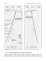
Varying
KEor
8
are impor-
tant practical ways of distinguishing what is in the outermost atomic layers from
what is underneath.
Instrumentation
An
XPS
spectrometer schematic is shown in Figure
7.
The X-ray
source
is usually
an
Al-
or
Mg-coated anode struck by electrons from
a
high voltage
(1
0-1
5
kv)
Alka
or
Mgka radiation lines produced at energies of
1486.6
eV and
1256.6
eV,
with line widths of about
1
eV. The
X
rays flood a large area
(-
1
cm2). The beam's
spot size
can
be improved
to
about
1OO-pm
diameter by focusing the electron beam
292
ELECTRON EMISSION SPECTROSCOPIES Chapter 5
1000
1
100
-a
10
Figure
6
I
I
1
10
100
1000
I
KE(eV)
-a
t'
-
000
100
10
Inorganic
cpds
\
1
10
100 1000
KE(eV)
-
Mean free path lengths
&
as
a
function
of
K€,
determined for (a) metals and
(b)
inorganic compounds.6
onto the anode and passing the X rays through an X-ray monochromator. The lat-
ter also improves line widths to between
0.5
and
0.25
eV, leading
to
higher resolu-
tion spectra
(thus
improving the chemical state identification process) and
removing an unwanted X-ray background at lower energies.
Practical limits
to
the shape and size of samples are set by commercial equipment
design. Some will take only small samples (e.g.,
1
cm
x
1
cm) while others can han-
dle whole 8-in computer disks. Flat samples improve signal strength and allow
quantitative
e
variation, but rough samples and powders are also routinely handled.
Insulating samples may charge under the X-ray beam, resulting in inaccurate
BE
determinations
or
spectra distorted beyond use. The problem can usually be miti-
gated by use of a low-energy electron flood gun to neutralize the charge, provided
this does not damage the sample.
The electron lenses
slow
th'e
electrons before entering the analyzer, improving
energy resolution. They are also used to define an analyzed area on the sample from
which electrons are received into the analyzer and, in one commercial design, to
image the sample through the analyzer
with
1O-pm tesolution. Older instruments
may have slits instead of lenses. The most popular analyzer is the hemispherical sec-
tor, which consists of
two
concentric hemispheres with a voltage applied benveen
them. This
type
of
analyzer is naturally suited
to
varying
8
by rotating
the
sample,
Figure
7.
The
XPS
spectrum is produced by varying
the
voltages on the lenses and
the analyzer
so
that the trajectories of electrons ejected from the sample at different
energies are brought, in turn,
to
a focus at the analyzer exit slit.
A
channeltron type
electron multiplier behind the exit slit
of
the analyzer amplifiers individual elec-
trons by 105-106, and each such pulse is fed
to
external conventional pulse count-
ing electronics and on into a computer. The computer also controls the lens and
5.1
XPS
293
Pul
e
Electronics
Counhg
.
UHV Chamber
Computer
D
Voltage Controls
to Lenses, Analyzer
UHV Chamber
A-
Computer Voltage Controls
to Lenses, Analyzer
Figure
7
Schematic
of
a
typical electron
spectrometer
showing all the necessary com-
ponents.
A
hemispherical electrostatic electron energy analyser
is
depicted.
analyzer voltages.
A
plot of electron pulses counted against analyzer-lens voltage
gives the photoelectron spectrum. More sophisticated detection schemes replace
the
exit
stir-multiplier arrangement with a multichannel array detector.
This
is the
modern equivalent
of
a photographic plate, allowing
simultaneous
detection
of
a
range
of
KEs,
thereby speeding
up
the detection procedure.
Commercial spectrometers are usually bakeable, can reach ultrahigh-vacuum
pressures
of
better than
1
O-g
Torr,
and have fast-entry load-lock systems
for
insert-
ing samples. The reason
for
the ultrahigh-vacuum design, which increases cost con-
siderably, is that reactive sudkces, e.g.,
dean
metals, contaminate rapidly in poor
yacuum
(1
atomic layer in
1
s
at
1
O4
Torr).
If the purpose
of
the spectrometer
is
to
always
look
at
as-inserted
samples,
which are already contaminated,
or
to examine
rather unreactive surfices (e.g., polymers) vacuum conditions can be relaxed con-
siderably.
294
ELECTRON EMISSION SPECTROSCOPIES Chapter
5
Applications
XPS
is routinely used in industry and research whenever elemental
or
chemical state
analysis is needed at
surfaces
and interfaces and the spatial resolution requirements
are not demanding (greater than
150
v).
If the analysis is related specifically to the
top 10
or
so
atomic layers of air-exposed sample, the sample is simply inserted and
data den. Examples where this might be appropriate include: examination for and
identification of surface contaminants; evaluation of materials processing steps,
such
as
cleaning procedures, plasma etching, thermal oxidation, silicide thin-film
formation; evaluation of thin-film coatings
or
lubricants (thicknessquantity,
chemical composition); failure analysis for adhesion between components, air oxi-
dation, corrosion, or other environmental degradation problems, tribological
(wear) activity; effectiveness of surface treatments of polymers and plastics; surface
composition differences for alloys; examination of catalyst surfaces before and after
use, after “activation” procedures,
and
unexplained hilures.
Figure 3c was used to illustrate that Si’” could be distinguished from Sio by the
Si 2p chemical shift. The spectrum is actually appropriate for an oxidized Si wafer
having an
-
10-A
Si02 overlayer. That the Si02 is an overlayer can easily be proved
by decreasing
8
to increase the surfgce sensitivity; the Sio signal will decrease relative
to rhe Siw signal. The
10-A
thickness can be determined from the Si”/Si0 ratio
and Equation (3), using the appropriate
4
value. That the overlayer is Si02 and
not some other Si’” compound is easily verified by observing the correct position
(BE)
and intensity of the
0
1s
peak plus the absence of other element peaks. If the
sample has been exposed to moisture, including laboratory air, the outermost
atomic layer will actually be hydroxide, not oxide. This is easily recognized since
there is a chemical shift between
OH
and
0
in the
0
1s
peak position.
Figure
8
shows a typical example where surface modification to a polymer can be
f~llowed.~ High-density polyethylene
(CHlCH,),
was surface-fluorinated in a
dilute fluorine-nitrogen mixture. Spectrum
A
was obtained after only
0.5
s
treat-
ment.
A
F
1s
signal corresponding to about a monolayer has appeared, and CF for-
mation is obvious from the chemically shifted shoulder
on
the
C
1s
peak at the
standard CF position. After
30
s
reaction, the F
1s
/
C
1s ratio indicates
(spectrum
B)
that the reaction has proceeded to about
30
A
depth, and that CF2
formation has occurred, judging by the appearance of the C
1s
peak at 291 eV.
Angular studies and more detailed line shape and relative intensity analysis, com-
pared to standards, showed that for the
0.5-s
case, the top monolayer is mainly
polyvinyl fluoride
(CFHCHZ),,
whereas after
30
s
polytrifluoroethylene
(CFZCFH), dominates in the top
two
layers. While this
is
a
rather aggressive exam-
ple of surface treatment of polymers, similar types of modifications frequently are
studied using
XPS.
An equivalent example in the semiconductor area would be the
etching processes of Si/SiO2 in CF4/02 mixtures, where varying the CFs/02 ratio
changes the relative etching rates of Si and Si02, and also produces different and
varying amounts
of
residues at the wafer’s surface.
5.1
XPS
295
A
691
687
CH
1
289
285
BE(eV)
Figure
8
XPS
spectrum in the
C
Is
and
F
1s
regions
of
polyethylene
(CH2).,
treated
with
II
dilute
Fz/N2
gaseous
mixture
for
(a)
0.5
set,
and
(b)
30
set?
In many applications the problem or prop- concerned is not related
just
to
the top
10
or
so
atomic layers. Information from deeper regions is required
for
a
number
of
reasons:
A
thick contaminant layer,
caused
by air exposure, may have
covered up the
s&
of interest; the material may
be
a
layered
structure in
which
the buried interfaces are important; the composition modulation with depth may
be important,
etc.
In such
cases,
the
2-1
5
atomic layer depth resolution attainable
in
XPS
by varying
8
is
insufficient, and some physical
means
of
stripping the
su&
while taking data, or prior to taking data, is required. This problem is common
to
all
very
surfice sensitive spectroscopies. The most widely
used
method is argon ion
sputtering, done inside the spectrometer while taking data. It
can
be
used
to depths
of
pm, but
is
most effective and generally
used
over mudl shorter
distances
(hun-
dreds and thousands of
Hi>
because it can be
a
slow
process and because sputtering
introduces artifacts that get worse
as
the sputtered depth increases.8 These indude
interf$cial mixing caused by the movement of atoms under the
Ar'
beam,
elemental
composition alteration caused by preferential sputtering
of
one element versus
another, and chemical changes caused by bonds being broken by the sputtering
ProCeSS.
If
the interface
or
depth of interest is beyond the capability
of
sputtering, one
can
try polishing down, sectioning, or chemical etching the sample before insertion.
296
ELECTRON EMISSION SPECTROSCOPIES Chapter 5
The effectiveness of this approach varies enormously, depending on
the
material,
as
does the extent of the damaged region left at the surface after this preparation treat-
ment.
In some cases, the problem
or
property of interest can be addressed only by per-
forming experiments inside the spectrometer.
For
instance, metallic
or
alloy
embrittlement can be studied by fracturing samples in ultrahigh vacuum
so
that the
fractured sample surface, which may reveal why the fracture occurred in that
region, can be examined without
air
exposure. Another example is the simulation
of
processing steps where exposure to air does not occur, such as many vacuum depo-
sition steps in the semiconductor and thin-film industries. Studying the progressive
effects of oxidation on metals
or
alloys inside the spectrometer is a fiirly well-estab-
lished procedure
and
even electrochemical cells are now coupled to
XPS
systems to
examine electrode surfaces without air exposure. Sometimes materials being pro-
cessed can be capped by deposition of inert material in the processing equipment
(e.g.,
Ag,
Au,
or
in
GaAs
work, arsenic oxide), which is then removed again by sput-
tering or heating after transfer to the
XPS
spectrometer. Finally, attempts are some-
times made to use “vacuum transfer suitcases” to avoid
air
exposure during transfer.
Comparison with other Techniques
XPS,
AES,
and SIMS are the three dominant surface analysis techniques.
XPS
and
AES
are quite similar in depth probed, elemental analysis capabilities, and absolute
sensitivity. The main
XPS
advantages are its more developed chemical state analysis
capability, somewhat more accurate elemental analysis, and far fewer problems
with induced sample damage and charging effects for insulators.
AES
has the
advantage of much higher spatial resolutions (hundreds of
A
compared to tens of
pm), and speed. Neither is good at trace analysis, which is one of the strengths of
SIMS (and related techniques). SIMS also detects
H,
which neither
AES
nor
XPS
do, and probes even less deeply at the surface, but is an intrinsically destructive
technique. Spatial resolution is intermediate between
AES
and
XPS.
ISS is the
fourth spectroscopy generally considered in the “true surface analysis” category. It is
much less used, partly owing to lack of commercial instrumentation, but mainly
because it is limited to elemental analysis with rather poor spectral distinction
between some elements. It is, however, the most surface sensitive elemental analysis
technique, seeing only the top atomic layer.
With
the exception
of
EELS and
HEELS,
all other spectroscopies used for surface analysis are much
less
surface
sensitive than the above four. HEELS is
a
vibrational technique supplying chem-
ical functional group information, not elemental analysis, and EELS is a rarely used
and specialized technique, which, however, can detect hydrogen.
5.1
XPS
297
Conclusions
XPS
has developed into the most generally used of the truly surface sensitive tech-
niques, being applied now routinely for elemental and chemical state analysis over a
range of materials in a wide variety of technological and chemical industries. Its
main current limitations are the lack of high spatial resolutions and relatively poor
absolute sensitivity (i.e., it is not a trace element analysis technique). Recently
introduced advances in commercial equipment have improved speed
and
sensitiv-
ity by using rotating anode X-ray sources (more photons) and parallel detection
schemes. Spot sizes have been reduced from about
150
pm, where they have lan-
guished for several years, to
75
pm. Spot sizes of 10 pm have been achieved, and
recently anounced commercial instruments offer these capabilities. When used in
conjunction with focused synchrotron radiation in various “photoelectron micro-
scope” modes higher resolution is obtainable. Routinely available
1
pm
XPS
resolu-
tion in laboratory-based equipment would be a major breakthrough, and should be
expected within the next three years.
Special, fully automated one-task
XPS
instruments are beginning to appear and
will find their way into both quality control laboratories and process control on
production lines before long.
More detailed discussions of
XPS
can
be found in references 4-12, which
encompass some of the major reference texts in this area.
Related Articles in the Enc ydopedia
UPS,
AES,
SIMS, and
ISS
References
I
K.
Siegbahn et
al.
ESG4:
Atomic,
Molecular,
andSolid State
Structure
Stud-
ied
by
Means
ofElectron
Spectroscopy.
Nova Acta Regime
SOC.
Sd.,
Upsa-
liensis, 1967, Series IV, Volume
20;
and
K.
Siegbahn et al.
ESU
Applied to
Free
Molecules.
North Holland, Amsterdam, 1969. These
two
volumes,
which cover the pioneering work of K.Siegbahn and coworkers in develop-
ing and applying
XPS,
are primarily concerned with chemical structure
identification of molecular materials and
do
not specifically address
sur-
face analysis.
2
Charts such as this, but in more detail, are provided by all the
XPS
instru-
ment manufacturers. They are based on extensive collections of data,
much of which comes from Reference
1.
3
J.
H.
Scofield.
J
Electron
Spect.
8,129,
1976.
This is the standard quoted
reference for photoionization cross sections
at
1487
eV.
It is actually one
of
the most heavily cited references in physical science. The calculations are
published in tabular form for all electron level
of
all elements.
298
ELECTRON EMISSION SPECTROSCOPIES Chapter
5
See, for example,
S.
Evans
et
a1.J
Elem Speck
14,341, 1978. Relative
experimental ratios of cross sections for the most intense peaks of most ele-
ments are given.
5
J.
C.
Carver,
G.
K.
Schweitzer, andT.
A.
Car1son.J
Chm.
Phys.
57,973,
1972. This paper deals with multiplet splitting
effects,
and their use in dis-
tinguishing different element states, in transition metal complexes.
6
M.
E
Seah and
W.
A.
Dench.
Su$
Inte6a.e
Anal.
1,
1,1979. Of the many
compilations of measured mean free path length versus
m,
this is the
most thorough, readable, and useful.
7
D.
T.
Clark,
W.
J.
Feast,
W
K.
R
Musgrave, and
I.
Ritchie.
J
Polym.
Sri.
Polym.
Chem.
13,857, 1975. One of many papers from Clark's group of
this era which deal with
all
aspects of
XPS
of polymers.
8
See the article on surface roughness in Chapter 12.
9
The book series
Electron Spectroscopy: Theory, Techniques, andApplications,
edited by
C.
R. Brundle and
A.
D.
Baker, published by Academic Press has
a
number of chapters in its
5
volumes which are usefd for those wanting
to
learn about the analytical use of
XPS:
In Volume 1,
An Introduction
to
Ekctron
Spectroscopy
(Baker and Brundle); in Volume
2,
Basic
Concepts of
XPS
(Fadley); in Volume
3,
AnalyticalApplicationr ofxPS
(Briggs); and in
Volume 4,
XPSfor
the
Investigation ofPolymeric Materialj
(Dilks).
io
T.
A.
Carlson,
Photoelectron andAuger Spectroscopj
Plenum, 1975.
A
complete and largely readable treatment of both subjects.
11
PracticaISufaceAmlysis,
edited by
D.
Briggs and
M.
E
Seah, published by
J.
Wiley;
Handbook ofXPSand
UPS,
edited by
D.
Briggs. Both contain
extensive discussion on use of
XPS
for surfice and material analysis.
12
Handbook
ofxPS,
C.
D.
Wagner, published by
PHI
(Perkin Elmer). This
is
a
book of
XPS
data, invaluable
as
a
standard reference source.
5.1
XPS
299
5.2
UPS
Ultraviolet Photoelectron Spectroscopy
C.
R.
BRUNDLE
Contents
Introduction
Basic Principles
Analysis Capabilities
Conclusions
Introduction
The photoelectric process, which was discovered in the early 1900s was developed
as
a means
of
studying the electronic structure
of
molecules in the gas phase in the
early 1960s, largely owing to the pioneering work
of
D.
W.
Turner's group.'
A
major step
was
the introduction
of
the He resonance discharge lamp
as
a laboratory
photon source, which provides monochromatic 2 1.2-eV light. In conjunction with
the introduction
of
high resolution electron energy analyzers, this enables the bind-
ing energies
(BE)
of
all
the electron energy levels below 21.2 eV to be accurately
determined with sufficient spectral resolution
to
resolve even vibrational excita-
tions. Coupled with theoretical calculations, these measurements provide informa-
tion on the bonding characteristics
of
the valence-level electrons that hold
molecules together. The area has become known
as
ultraviolet photoelectron spec-
troscopy
(UPS)
because the photon energies used (21.2 eV and lower) are in the
vacuum ultraviolet
(UV)
part
of
the light spectrum. It is also known
as
molecular
photoelectron spectroscopy, because
of
its ability to provide molecular bonding
information.
In parallel with these developments for studying molecules, the same technique
was being developed independently to study solids: particularly metals and semi-
300
ELECTRON EMISSION SPECTROSCOPIES Chapter
5
conductors.’ This branch of the technique
is
usually known
as
UV
photoemission.
Here the electronic structure
of
the solid (the band structure for meds and semi-
conductors) was the interest. Since the technique
is
sensitive to only the top few
atomic layers, the electronic structure
of
the surfice, which in general
can
be differ-
ent from that
of
the bdk, is actually obtained. The
two
branches of
UPS,
gas-phase
and solid-surface studies, come together when adsorption and reaction of molecules
at surfices is studied?.
Though commercial
UPS
instruments were sold in
the
1970s,
for gas-phase
work, none are sold today. Since the only additional item required to perform
UPS
on an
XPS
instrument is a He source, this is usually how
UPS
is performed in the
laboratory.
An
alternative, more specialized approach,
is
to couple an electron spec-
trometer to the beam-line monochromator
of
a synchrotron ficility.
This
provides
a tunable source
of
light, usually between around
10
eV and
200
eV, though
many
beam lines can obtain much higher energies. This approach can provide a number
of advantages, including variable surface sensitivity and access to core levels up to
the photon energy used, at much higher resolution than obtainable by laboratory
XPS
instruments. Even using a laboratory
UPS
source, such
as
a He resonance
lamp,
some low-Iying core
levels
are accessible. When using either synchrotron
or
laboratory
sources
to access
core
levels,
all
the materials
surface
analysis capabilities
of
XPS
described in the preceding article become available.
Basic
Principles
The photoionization process and the way it is
used
to measure
BEs
of electrons to
afoms is described in the article on
XPS
and will not be repeated here. Instead, we
will concentrate on the differences between the characteristics
of
core-level
BEs,
described in the
XPS
article, and those of valence-level
BEs.
In
Figure la the elec-
tron energy-level diagram
for
a
CO
molecule is shown, schematically illustrating
how the atomic levels of the
C
and
0
atom interact to fbrm
the
CO
molecule. The
important point
ro
note is that whereas the
BEs
of
the
C
1s
and
0
1s
core levels
remain characteristic
of
the atoms when the
CO
molecule is formed (the basis
of
the use
of
XPS
as
an elemental analysis
tool),
the
C
2p and
0
2p
valence levels are
no longer characteristic
of
the individual atoms, but have combined to form
a
new
set
of
molecular orbitas entirely characreristic
of
the
CO
molecule. Therefore, the
UPS
valence-band spectrum of the
CO
molecule, Figure lb, is also entirely charac-
teristic
of
the molecule, the individual presence
of
a
C
arom and an
0
atom no
longer being recognizable.
For
a
solid,
such
as
metallic Ni, the valence-level elec-
trons
are smeared
out
into a band,
as
can
be seen in the
UPS
spectrum
of
Ni (Figure
2a). For molecules adsorbed on surfaces there is also a smearing out
of
structure.
For example, Figure 2b shows a monolayer
of
CO
adsorbed on an Ni surface.
5.2
UPS
30;
-
ococ
UPS
Spectrum
(He11
t
38t
2u
t
-
1s
295
-
545
-
1U
1s
-
a
b
Figure
1
(a) Electron energy diagram
for
the
CO
molecule, illustrating how
the
molecular
orbitals are constructed from
the
atomic levels.
(b)
He
I
UPS
spectrum
of
CO.’
Analytical Capabilities
As
stated earlier, the major use of
UPS
is not for materials analysis purposes but
for
electronic structure studies. There are analysis capabilities, however. We will con-
sider these in
two
parts: those involving the electron valence energy levels and those
involving low-lying core levels accessible to
UPS
photon energies (including syn-
chrotron sources). Then we will answer the question “why use
UPS
if
XPS
is avail-
able?”
Valence Levels
The spectrum of Figure
1
b
is a fingerprint of the presence of a
CO
molecule, since
it
is different in detail from that of any other molecule.
UPS
can therefore be used
to identify molecules, either in the
gas
phase
or
present at surfaces, provided a data
bank of molecular spectra is available, and provided that the spectral features are
sufficiently well resolved
to
distinguish between molecules. By now the
gas
phase
spectra of most molecules have been recorded and can be found in the literature.
‘3
Since one is using
a
pattern of peaks spread over only a few eV for identification
purposes, mixtures of molecules present will produce overlapping patterns. How
well mixtures can be analyzed depends, obviously, on how well overlapping peaks
can
be resolved.
For
molecules with well-resolved fine structure (vibrational) in the
spectra (see Figure lb), this can be done much more successfully than for the broad,
302
ELECTRON EMISSION SPECTROSCOPIES Chapter
5