The Materials Science of Thin Films 2011 Part 11 pot
Bạn đang xem bản rút gọn của tài liệu. Xem và tải ngay bản đầy đủ của tài liệu tại đây (1.94 MB, 50 trang )
470
Electrical and Magnetic Properties
of
Thin Films
reason that technological interest has centered on insulating films employed in
microelectronics, notably the gate oxide, where dielectric breakdown is a
serious reliability concern. The remainder of this section will therefore
be
devoted to SiO, films (Ref. 19).
It is generally agreed that electron impact ionization is responsible for
intrinsic breakdown in SiO, films. In this process, electrons colliding with
lattice atoms break valence bonds, creating electron-hole pairs. These new
electrons accelerate in the field and through repeated impacts generate more
electrons. Ultimately a current avalanche develops that rapidly and uncontrol-
lably leads to excessive local heating and dielectric failure. Typical of theoreti-
cal modeling (Refs.
19, 20) of breakdown is the consideration of three
interdependent issues;
Electrode charge injection into the insulator, e.g., by tunneling (Eq. 10-22).
This formula connects current and applied field.
The local electric field that is controlled by the relatively immobile hole
density through the Poisson equation.
A
time-dependent change in hole density that increases with extent of
impact ionization, but decreases with amount of hole recombination or drift
away. The resulting rate equation depends on both current and field.
Simultaneous satisfaction of these coupled relationships leads to the predic-
tion that the current-voltage characteristics display negative resistance. This
appears as a knee in the response above a critical applied voltage and reflects
a current runaway instability. Another prediction is that the average break-
down field rises sharply as the film thickncss decreases.
Reliability concerns for thin SiO, films in
MOS
transistors have fostered
much statistical analysis of life-testing results and some typical experimental
findings include:
1.
2.
3.
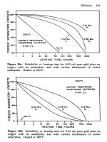
The histogram of the number of breakdown failures due to intrinsic causes
peaks sharply at about 1.1
x
lo7
V/cm (Fig. 10-14a). The failure probabil-
ity is nil below 7
x
IO6 V/cm.
Time to failure (TTF) accelerated testing has revealed that
0.33
eV
kT
TTF
a
exp- exp
-
2.47 V, (10-32)
where the exponentials represent individual temperature and voltage accel-
eration factors (Ref. 21).
Contrary to theory, thinner oxides present a greater failure risk. The
lifetime dependence on oxide film thickness is shown in Fig. 10-14b. Note
10.4.
Semiconductor Contacts and
MOS
Structures
479
300
270
240
5
210
5
180
8
150
pj
120
g90
3
260
30
n
L
0
24
6
8
10
12
14
E
(MV/cm)
(a)
104
STRESS
FIELD
:
8
MV
Icm
CUMULATIVE
PERCENT
(b)
Figure
10-14.
(a)
Histogram
of
number
of
failures versus applied electric field
in
thin
SO,
films. (From
D.
R.
Wolters and
J. J.
van der Schoot,
Philips
J.
Res.
40,
115,
1985).
(b)
Time-dependent dielectric breakdown in SO,. (Courtesy
of
A.
M-R
Lin, AT&T Bell Laboratories.)
480
Electrical and Magnetic Properties
of
Thin
Films
that a 100-i difference in film thickness signifies a four-order-of-magnitude
change in failure time.
4. Film defects cause breakdown to occur at smaller than intrinsic fields and in
correspondingly shorter times.
As
an example illustrating the use of
Eq.
10-32 assume that the lifetime
of SiO, films is 100 h during accelerated testing at 125
“C and 9
V.
What lifetime can be expected at 25 “C and
8
V? Clearly, TTF
=
l0Oexp0.33/k(l/T2
-
l/T,)exp
-
2.47(V2
-
V,),
where
T2
=
298,
T,
=
398,
V,
=
8,
V,
=
9,
and
k
=
8.63
x
eV/K. Substitution yields a
value for
TTF
=
29,700 h.
10.5.
SUPERCONDUCTIVITY IN
THIN
FILMS
10.5.1.
Overview
The discovery in 1986- 1987 that superconductivity is exhibited by oxide
materials at temperatures above the boiling point
of
liquid nitrogcn ignited
intense worldwide research devoted to understanding and exploiting the phe-
nomenon. For a perspective of superconducting effects
in
these new materials
and prospects for thin-film
uses,
it
is worthwhile to view the subject against the
75-year backdrop of prior activity. This pre-1988 “classical” experience with
superconductivity will therefore be surveyed first
in
this chapter (Ref. 22); in
Chapter 14 high-temperature superconductivity will be discussed.
Superconductivity was discovered by Kamerlingh Onnes, who, in 191
1,
found that the electrical resistance of Hg vanished below 4.15
K.
Actually it
was estimated from the time decay of (nearly) persistent supercurrents in a
toroid that the resistivity of the superconducting state does not exceed
-
lo-’’
Q-cm, some 14 orders
of
magnitude below that for Cu. Some basic attributes
possessed by superconductors have been experimentally verified and theoreti-
cally addressed over the years. These are briefly enumerated here.
1.
Occurrence
of
Superconductivity.
The phenomenon of superconductiv-
ity
has
been observed
to
occur
in at
least
26
elements and
in
hundreds and
perhaps thousands of metallic alloys and compounds. It is favored by a large
atomic volume
or
lattice parameter, and when there are between two and eight
valence electrons per atom.
2.
Critical Temperature and Magnetic Field.
The superconducting state
only exists in a specific range of temperature
(T)
and magnetic field strength
10.5.
Superconducitivity In Thin Films
481
Table
10-3.
Values
of
T,
and
H,
for
Superconducting
Materials
Alloy
Element
T,
(K)
H,
(a)
or
Compound
T',
(K)
Hs
(a)**
~~
AI
1.19
In
3.41
UP)
5.9
N-b
9.2
Pb
7.18
Re
1.70
Sn
3.72
Ta
4.48
Tc
8.22
Th
1.37
TI
2.39
V
5.13
98.8
285
lo00
800
200
308
825
2,o00*, 3,o00**
161
170
1290*, 7000**
v3Ga
V3Si
Nb,Sn
Nb3a
M3Ge
PbMO,S,
NbN
YBa,Cu
,O,
BiSrCaCuO
TlBaCaCuO
14.8 25
X
lo4
16.9 24
X
lo4
18.3
28
X
lo4
20.2 34
x
io4
22.5 38
x
lo4
14.4
60
x
io4
15.7
15
x
lo4
93
-
107
-
120
-
(HI.
Critical values
of
these
quantities are experimentally found to be closely
described by
(10-33)
where
H,
is the critical field,
No
is the maximum field at
T
=
0
K,
and
T,
is
the highest temperature at which superconductivity is observed.
On
an
H
vs.
T
plot the division between superconducting and
normal
conduction regimes is
defined by
Eq.
10-33.
A
temperature spread of only
-
K K
in
pure metals,
lo-'
K
in alloys) about the
value
of
T,
characterizes
the
sharpness
of
the transition between the
two
states. Superconductivity can
be
extinguished by exposure to a field greater
than
H,
or
by passing a
supercur-
rent that induces a magnetic field in excess
of
H,.
Values
of
T,
and
H,
are
listed in Table
10-3
for
a
number of superconducting materials.
3.
Meissner
Effect.
One
of
the remarkable features
of
the superconducting
state
is
the
Meissner effect. It
is
characterized by the exclusion
of
magnetic
flux
and,
hence, electrical currents
from
the
bulk
of the superconductor. The
exclusion is not total, however, and
both
flux and current
are
confined to a
surface layer known as the penetration depth
A,.
The London theory
of
superconductivity indicates that
(
10-34)
482
Electrical
and
Magnetic
Properties
of
Thin Films
where
A,y(0)
is the penetration depth at 0
K.
Typically,
A,
is
500-1000
A.
The
Meissner effect means that
if
a superconductor is approached by an
H
field,
screening currents are set up on its surface. This screening current establishes
an equal and opposite
H
field
so
that the net field vanishes in the supercon-
ductor interior. The now common displays of permanent magnets levitated
over chilled high-T, superconductors is visual evidence of the Meissner effect.
4.
Type
Z
and
Type
ZZ
Superconductors.
There are two types of supercon-
ductors: type I (or
soft)
and type I1 (or hard). With the exception of
Nb
and
V
the elements are type
I
superconductors. In such materials the superconducting
transition is abrupt, and flux penetrates only for fields larger than
H,
.
In type
I1 superconductors (exemplified by Nb,
V,
alloys (e.g., Mo-Re, Nb-Ti), and
A-15 compounds (e.g., Nb,Sn, Nb,Ge)), there are two critical fields
H,(I)
and
HJu),
the lower and upper values. If the applied field is below
Hs(/),
type I1 behavior
is
the same as that displayed by type
I
superconductors. For
fields above
HJI)
but below
HJu),
there is a mixed superconducting state,
whereas for
H
>
H,(u),
normal conductivity is observed. Importantly, type I1
superconductors can survive in the mixed state up to extremely high
H
values
(e.g., in excess
of
lo5
gauss).
This property has earmarked their use in
commercial superconducting magnets. In the mixed state, just above
Hs([),
flux
starts to penetrate the material in microscopic tubular filaments
(-
loo0
in diameter), known as fluxoids or vortices, that lie parallel to the field
direction. The core of the fluxoid is normal while the sheath is superconduct-
ing; the circulating supercurrent of the latter establishes the field that keeps the
core normal. Fluxoids, which are usually arranged in a lattice array, grow in
size as the field is increased with progressively more flux penetration. Above
H,(
u),
flux
penetrates everywhere. The current flow is not entirely lossless
in
the mixed state, however, because a small amount
of
power is dissipated by
viscous fluxoid motion. Fluxoid pinning due to introduction of alloying ele-
ments
or
defects is a practical way to minimize this energy loss.
5.
The
BCS
Theory.
The theory by Bardeen, Cooper, and Schrieffer (BCS)
(Ref.
24)
in 1957 provided the basis for understanding superconductivity at a
microscopic level, superceding previous phenomenological approaches. Cen-
tral
to
the
BCS
theory is the complex coupling between a pair of electrons of
opposite spin and momentum through an interaction with lattice phonons. The
electrons that normally repel each other develop a mutual attraction, forming
Cooper pairs. A measure of the average maximum length at which the phonon
coupled attraction can occur
is
known as the coherence length
5.
Schrieffer
described the theoretical issue as “how to choreograph a dance for more than a
million, million, million couples”
so
that they condense into a single state that
10.5.
Supelconducitivlty in
Thin
Films
483
moves in step or flows like a frictionless fluid (Ref.
24).
Since the electron
coupling is weak, the energy difference between normal and superconducting
states is small with the latter lying a
distance
2A
below the former.
Thus,
a
forbidden energy gap of width
2A
=
3.5kT,
(10-35)
appears in
the
density
of
states centered about the Fermi energy at
0
K.
This
predicted relationship has been verified in many superconductors by tunneling
measurements, which are described in the next section.
When the temperature is raised, the amplitude and frequency
of
lattice
atomic motion increase, interfering with the propagation of phonons between
correlated Cooper pairs. The attraction between electrons is diminished and
2A
decreases. At
T
=
T,,
A
=
0.
Any perturbation in structure or composition
extending over the coherence length can alter
T,
or
2A,
placing a practical
limit on useful superconducting behavior.
10.5.2.
Superconductivity in Thin Films; Tunneling
Thin films have traditionally played a critical role in testing theories of
superconductivity and in establishing new effects. Superconductivity appar-
ently persists to film thicknesses of
-
10
A.
Lower limits
are
difficult to
establish because films of such thickness
are
generally discontinuous. The
dependence
of
T,
on deposition conditions and film thickness has been studied
for a long time, and interesting, though not easily predictable or explainable,
effects have been reported. When either
A,
or
t
becomes comparable to the
thin film thickness, deviation from bulk superconducting properties may be
expected. For example, enhanced superconductivity has been reported
in
vapor-quenched, amorphous Bi and Be films where
T,
values of
6
and
8
K
were obtained, even though these metals are not superconducting in bulk.
Higher
T,
values with decreasing film thickness have been observed by
several investigators. The size
of
these effects ranges from fractions to several
degrees
K
and depends on the magnitude and sign
of
the film stress, impuri-
ties, lattice imperfections, and grain size in generally inexplicable ways.
A
link
between
T,
and the fundamental nature of the material is suggested
by
the BCS
formula
1.14hv
1
T,
=
~
exp
-
k
N(EFP
(10-36)
(for
N(
EF)U
-4
1).
The quantity
N(EF)
is
the
density
of
states at the Fermi
level,
U
is the magnitude of the attractive electron-lattice interaction, and
v
corresponds to the lattice (Debye) frequency. Normally
N(EF)U
is weakly
484
Electrical and Magnetic Properties
of
Thin Films
sensitive to lattice dimensions and has a value between
0.1
to
0.5.
Furthermore
if
N(E,),
U,
or
v
increase,
so
does
T,.
However, connections between these
quantities, on the one hand, and film composition and structure, on the other,
are uncertain at best.
The most extensive experimentation in thin films has involved tunneling
phenomena. Unlike the tunneling between normal metals considered earlier
(Section
10.3.1),
a superconducting tunnel junction consists of two metal
films, one or both being a superconductor, separated by
an
ultrathin oxide or
insulator film. Tunneling currents generally flow when electrons emerge from
one metal
to
occupy allowable empty electron states of the same energy in the
opposite metal. Through application of voltage bias, relative shifts of the entire
electron distribution of both metals occur, either permitting or disallowing
tunneling transitions. Thus, if electrons at the Fermi level of a normal
metal
lie
opposite the forbidden energy gap at the Fermi level of the superconductor, no
tunnel current flows. Translation
of
band states by
a
voltage
A
/q,
or half the
energy gap, causes occupied energy levels of the former to line
up
with
unoccupied levels
of
the latter resulting in current flow.
If
both electrodes are
the same superconductor, a voltage corresponding to the whole energy gap
must
be applied before tunnel current
flows.
Current-voltage characteristics
corresponding to these two cases are shown in Fig. 10-15.
A
more complicated
behavior is exhibited when two different superconductors with energy gaps
Figure
1
0-1
5.
Current-voltage characteristics
of
tunnel junctions: tunnel
junctions
(a)
one
metal
normal-one
metal
superconducting.
@)
both metals identical supercon-
ductors.
(c)
both
metals
superconducting but with different energy gaps.
(d)
Josephson
tunneling
branch
(1)
and
normal
superconducting tunneling branch
(2).
J,
is the critical
junction
current
density.
10.6.
Introduction to Ferromagnetism
485
2A,
and
26,
are paired. By yielding precise values of
2A,
such measurements
have provided direct experimental verification
of
the BCS theory.
One
of
the very important advances in superconductivity was the remarkable
discovery by Josephson (Ref.
25)
that supercurrents can tunnel through a
junction. Thus tunneling of Cooper pairs and not only electrons is possible.
Two superconducting electrodes sandwiching an ultrathin insulator
-
50
thick are required. The current-voltage characteristic has
two
branches (Fig.
10-15d). The normal tunneling branch is similar to Fig. 10-15 but with a
reduced negative resistance feature. The Josephson tunneling current branch
consists of a current spike; no voltage develops across the superconducting
junction in this case. Because
the
Josephson current is extremely sensitive to
H
fields, the junction can
be
easily switched from one branch to the other.
Josephson devices known as SQUIDS (superconducting quantum interfer-
ence devices) capitalize on these effects to detect very small
H
fields or to
switch currents at ultrahigh speed in computer logic circuits. These applica-
tions will be described in more detail in Section
14.8.3.
1
0.6.
INTRODUCTION
TO
FERROMAGNETISM
The remainder of this chapter is devoted to some
of
the
ferromagnetic
properties
of
thin films (Refs.
26,
27). We start with the idea that magnetic
phenomena have quantum mechanical origins stemming from the quantized
angular momentum of orbiting and spinning atomic electrons. These circulat-
ing charges effectively establish the equivalent of microscopic bar magnets or
magnetic moments. When neighboring moments due to spin spontaneously and
cooperatively order in parallel alignment over macroscopic dimensions in
a
material to yield a large moment of magnetization
(M),
then we speak of
ferromagnetism. The quantity
M
is clearly a vector with a magnitude equal to
the vector sum of magnetic moments per unit volume. In an external magnetic
field
(H)
the interaction with
M
yields a field energy density
(EH)
given by
E,=
-H*M.
(10-37)
However, no external field need be applied to induce the ferromagnetic state.
The phenomenon of ferromagnetism has a number of characteristics and
properties
worth
noting at the outset.
1.
Elements (e.g., Fe, Ni,
Co),
alloys (e.g., Fe-Ni, Co-Ni), oxide insula-
tors (e.g., nickel-zinc ferrite, strontium ferrite) and ionic compounds (e.g.,
CrBr,, EuS,
Ed,)
all exhibit ferromagnetism. Not only are all crystal
486
Electrical and Magnetic Properlies
of
Thin
Films
structures and bonding mechanisms represented, but amorphous ferromagnets
have also been synthesized (e.g., melt-quenched Fe,,B,, ribbons and vapor-
deposited Co-Gd films).
2. Quantum mechanical exchange interactions cause the parallel spin align-
ments that result in ferromagnetism. It requires an increase in system energy to
disorient spin pairings and cause deviations from the parallel alignment direc-
tion. This energy, known as the exchange energy
(Eex),
is given by
E,,
=
A,(VdJ)*
(10-38)
and is a measure of the “stiffness” of
M
or how strongly neighboring spins
are coupled.
The
exchange constant
Ax
is a property of the material and equal
to
-
ergs/cm in Ni-Fe. Avoidance
of
sharp gradients in
4,
the angle
between
M
and the easy
axis
of
magnetization, leads to small values of
E,,
.
3.
Absorbed thermal energy serves to randomize the orientation of the spin
moments
ps
.
At
the Curie temperature
(T,)
the collective alignment collapses,
and the ferromagnetism
is
destroyed. By equating the thermal energy absorbed
to the internal field energy
(pJH,),
i.e.,
kT,
=
p,N,,
values of
H,
can
be
estimated. The internal field
U,
permeating the matrix is established by
exchange interactions. Typically,
H,
is
predicted to be in excess of
lo6
Oe, an
extremely high field.
4.
Magnetic anisotropy phenomena play a dominant role in determining the
magnetic properties of ferromagnetic films. By anisotropy we mean the
tendency
of
M
to lie along certain directions in a material rather than be
isotropically distributed.
In
single crystals,
M
prefers to lie in the so-called
easy direction, say
[loo]
in
Fe
and
[lll]
in Ni. To turn
A4
into other
orientations, or harder directions, requires energy (i.e., magnetocrystalline
anisotropy energy
(
EK)).
Consider now a fine-grained polycrystalline ferro-
magnetic film of Permalloy
(-
80
Ni-20 Fe). Surprisingly, it also exhibits
anisotropy with
M
lying in the film plane. In such a case
EK
is a function of
the orientation of
M
with respect to film coordinates. For uniaxial anisotropy
EK
=
K,sin20,
(10-39)
where
K,
is a constant with units of energy/volume, and
8
is
the
angle
between the in-plane saturation magnetization and the easy axis. The source
of
the anisotropy is not due to crystallographic geometry but rather to the
anisotropy arising from shape effects (Le., shape anisotropy).
When ferromagnetic bodies are magnetized, magnetic poles are created on
the surface. These poles establish a demagnetizing field
(
H,,)
proportional and
antiparallel to
M,
i.e.,
H,,
=
-
NM,
where
N
is known as the demagnetizing
10.6.
lntroductlon to Ferromagnetism
487
factor and depends on the shape of the body. For a thin film, N
=
47r
in the
direction normal to the film plane. Therefore,
Hd
=
-4rM.
In evaporated
Permalloy films
H,,
can
be
as large as
-
lo4
Oe.
However, in
the
film plane
H,,
is much smaller
so
that
M
prefers to lie in this plane. There are other
magnetic films of great technological importance-garnets for magnetic bubble
devices (Section 10.8.4) and Co-Cr for perpendicular magnetic recording
applications (Section 14.4.3)-where
M
is
perpendicular
to the film plane.
Associated with
Hd
is magnetostatic energy
(E,)
of amount
per unit volume. The
1/2
arises because self-energy is involved, i.e.,
Hd
is
created from the distribution of
M
in the film. In the hard direction the
energy density is therefore
EM
=
2uM2.
(1041)
The origins
of
anisotropy are complex and apparently involve directional
ordering
of
magnetic atom pairs, e.g., Fe-Fe. Film anisotropy
is
affected by
film deposition method and variables, impingement angle of the incident vapor
flux, applied magnetic fields during deposition, composition, internal stress,
EM=
(1/2)HdM
(
10-40)
M
t
HARD
/H,"
Figure
10-16.
Schematic hysteresis
loops
for
soft
and hard magnetic materials. For
soft
magnets
H,
5
0.05
Oe.
For hard magnets
H,
2
300
Oe. (From
Ref.
28).
488
Electrical and Magnetic Propertles
of
Thin
Films
and columnar grain morphology, in not readily understood
ways.
Even amor-
phous ferromagnetic
films
exhibit magnetic anisotropy.
5.
Not
all
ferromagnetic materials are magnets
or
have the ability to attract
other ferromagnetic objects. The reason
is
that the matrix decomposes into an
array of domains, each of which has a constant
M
but is differently oriented.
Hence,
EM
=
0
over macroscopic dimensions. Domains facilitate magnetic
flux closure and reduce stray external magnetic fields-effects that minimize
Table
10-4.
Properties
of
Soft
and Hard Magnetic
Thin
Films
Soft
Magnetic
Materials
4rMs
(kG)
H,
@e)
Hk
(Oe) Application
Permalloy
CoZr (amorphous)
Fe,B2, (amorphous)
Fe,,Si2, (amorphous)
Fe,,Si,,C
,,
(amorphous)
'3
FeSo
I2
Hard Magnetic
Materials
10
0.5
5
Computer memory,
magnetoresistance
detectors,
recording heads
14
<
0.5 2-5
-
15
0.04
7
12
0.2
4
16
0.2
7
-
-
-
1
-0
loo0
Magnetic
bubble memory
devices
6-9
10-18
10-15
5.5
5
3
3
4-1
-
10
700
1100-
1800
1DM)-
1300
650
300
700
2100
500-2DM)
H,
(perpendicular)
2000-loo00
1000-2000
1000-3000
Longitudinal
magnetic recording
media
Perpendicular
magnetic
recording media
Magneto-optic
recording media
~ ~
-
*Values
for
M,
and
H,
depend strongly on composition and method
of
deposition.
H,
(parallel) values
are
typically
0.5
H,
(perpendicular).
Note:
1
Oe
=
80
A/m;
1
G
=
From Refs.
28-30.
T;
Hk
(anisotropy field)
=
2K,/Ms
10.7.
Magnetic Film
Size
Effects
-
M,
vs.
Thickness and Temperature
489
EM.
In bulk materials, domains are frequently smaller than the grain size,
whereas the reverse is true in films.
The response of a ferromagnet to an externally applied magnetic field is its
most important engineering characteristic. Initially,
M
increases with
H
and
eventually levels off at the saturation magnetization value
M,.
The application
of
H
causes favorably oriented domains to grow at the expense of unfavorably
oriented ones by domain boundary migration. At high enough fields,
M
even
rotates. Further cycling of
H
in both positive and negative senses yields the
well-known hysteresis loop. Depending on its size and shape ferromagnets are
subdivided into two types-hard and
soft,
as indicated schematically in Fig.
10-16.
The distinction is based on the magnitude of the coercive force
H,
or
field required to reduce
M
to zero. Hard magnetic materials with large
H,
are
hard to magnetize and hard to demagnetize. That is why they make good
permanent magnets and are used for magnetic recording media.
Soft
magnetic
materials, on the other hand, both magnetize and switch magnetization direc-
tions easily (small
HJ.
These are just the properties required for computer
memory
or
recording head applications. In Table
10-4
the properties of both
soft
and hard magnetic thin-film materials are listed. How these ferromagnetic
properties are manifested in applications is explored in the remainder of this
chapter as well as in Chapter
14.
10.7.
MAGNETIC
FILM
SIZE EFFECTS
-
M,
vs.
THICKNESS
AND
TEMPERATURE
10.7.1.
Theory
Magnetic property size effects are expected simply because the electron spin in
an atom on the surface of a uniformly magnetized ferromagnetic film is less
tightly constrained than spins on interior atoms. Fewer exchange coupling
bonds on the surface than in the interior is the reason. Therefore, the question
has been raised of how thin films can be and still retain ferromagnetic
properties. At least four decades of both theoretical and experimental research
have been conducted on the many aspects of this fundamental issue and related
ones. The two theoretical approaches-spin wave and molecular field-both
predict that a two-dimensional network of atoms of ferromagnetic elements
should not be ferromagnetic but rather paramagnetic at absolute zero. At low
temperatures a ferromagnet has very nearly its maximum magnetization. The
deviation from complete saturation
(AM,)
is due to waves of reversed spin
propagating through the material.
By
summing
the
spin waves according to the
490
Electrical and
Magnetic
Properties
of
Thin
Films
D=
m
D
=
128
D=64
D=32
3=16
i
TEMPERATURE
(K)
(b)
Figure
10-1
7.
(a) Calculated temperature dependence of normalized saturation mag-
netization
for
different numbers of film layers
(D).
(From Ref.
31).
(b)
Temperature
dependence of relative bulk and surface magnetization
in
the ferromagnetic glass
Fe,Ni,B,
(From
Ref.
33).
10.7.
Magnetic Film
Size
Effects
-
M,
vs.
Thlckness and Temperature
491
rules of quantum statistical mechanics, we obtain the magnitude of the devia-
tion at any temperature
(AMJT))
relative to absolute zero
M,(O).
In bulk
materials it is generally accepted that
AM,(T)/M,(O)
=
BT3/*,
(10-42)
where
B
is the spin wave parameter. Its value at the surface has been
calculated to be twice that in
the
bulk. In thin films, theoretical treatments of
magnetic size effects are a subject of controversy. Early calculations show a
relative decrease in
A4
vs.
T
for films of varying thickness as indicated in Fig.
10-17.
For films thinner than four atomic layers
M3
varies linearly over a
wide temperature range.
The molecular field approach replaces the exchange interaction between
neighboring spins around a particular atom by an effective molecular field.
A
statistical accounting of the number of interactions between an atom in the jth
layer of a film with other atoms in the same
as
well as
j
-
1
and
j
+
1
layers
is the approach taken. Such calculations typically reveal that
M
begins to
decrease below the value in bulk when the film thickness is less than some
number of lattice spacings (e.g.,
IO),
corresponding to a film thickness of
perhaps
30
A.
In recent years, quantum calculations of ferromagnetic films have achieved a
high level of sophistication (Ref.
32).
Spin densities in the ground
state
of Fe
and Ni films consisting of
a
few atomic layers have, interestingly, been
predicted to lead to
an
enhancement
of
the magnetic moment per atom in the
outermost layer (e.g., by
20%
in (001)Ni and
34%
in (001)Fe compared
to
the
bulk value found four layers away). Such surprising results rule out the
existence of magnetically “dead” layers reported in the literature.
Importantly, none of the aforementioned theories explicitly takes into ac-
count such surface
effects
as lattice relaxation or distortion, surface reconstruc-
tion, and pseudomorphic growth at
real
surfaces and interfaces. Rather,
perfectly planar surfaces are assumed.
10.7.2.
Experiment
Many experimental methods have evolved to yield
direct
or
indirect
evidence
of ferromagnetic order in thin films. They broadly fall into three categories,
depending on whether
the
1.
spin polarization of electrons,
2.
net magnetic moment of the sample, or
3.
internal magnetic (hyperfine) field
492
Electrical and Magnetic
Properties
of
Thin
Films
is measured. The first relies on extracting electrons from the conduction bands
of ferromagnetic solids by photoelectron emission and analyzing their energies
by methods similar to those employed in Auger spectroscopy. Assuming no
spin flips occur during emission, the number of majority and minority spins
relative to the direction of magnetization of the surface can
be
determined. For
example, the net surface magnetization of Fe,,Ni,,B,,
,
an amorphous ferro-
magnet
(T,
=
700
K),
was measured by detecting elastically backscattered
spin polarized electrons (Ref.
33).
The results are depicted in Fig. 10-17b for
90
eV electrons which are estimated to probe only
the
topmost one or two
atomic layers
(-
2.5
A).
Method
2
relies on very sensitive magnetometers to
directly yield macroscopic
M
vs.
H
behavior. Although relatively free from
interpretation problems associated with indirect methods
1
and
3,
the measure-
ments are not surface selective. In the third method the hyperfine magnetic
field
Heff,
which is to a good approximation proportional to the local atomic
moment, is measured. Nuclear physics techniques such as nuclear magnetic
resonance and Mossbauer effect are
used;
only the latter will
be
discussed here
at any length.
The Mossbauer effect is based on the spectroscopy of specific low-energy
nuclear y-rays that are emitted (without recoil) from excited radioactive atoms
embedded
in
a
source. These y-rays are absorbed by similar nonradioactive
ground state atoms contained within an absorber matrix. In the most famous
Mossbauer transition,
57C0
nuclei emit 14.4-keV y-rays and decay to the 57Fe
ground state. An absorber containing 57Fe, an isotope present in natural Fe
with an atomic abundance of
2.2%,
can absorb the y-ray if its nuclear levels
are very precisely tuned to this exact energy. Otherwise there is no absorption,
and the y-ray will simply pass through the absorber and be counted by a y-ray
detector. This is usually the case because differences in the local electromag-
netic environment of FeS7 in both the source and absorber alter the 14.4-keV
level slightly, destroying the resonance. Fortunately very small, easily pro-
duced Doppler effect energy shifts, caused by relative source-absorber veloci-
ties of only
-
k
1
cm/sec, can increase or decrease the energy sufficiently to
restore the resonance. Mossbauer spectra thus reveal relative energy differ-
ences in y-ray transitions of 57Fe
as
they
are
affected by atomic surroundings.
In
a
ferromagnetic absorber the 57Fe nucleus is immersed in the internal
magnetic field that splits the nuclear levels, an effect that is the counterpart to
Zeeman splitting of atomic electron levels. Six transitions can now be accessed
by using an appropriate (unsplit) source.
Mossbauer spectra of Fe film absorbers of varying thickness grown epitaxi-
ally on Ag are shown in Fig. 10-18. The detection of y-ray-induced conversion
electrons plus the use of enriched 57Fe layers provide the necessary sensitivity
10.8.
Magnetic Thin Flims
for
Memory
Applications
493
I
1
-6
-4
-2
0
2
4
6
V
[
mmls
J
Figure
10-1
8.
Mossbauer spectra
of
ultrathin epitaxial (1 10) Fe
films
on
(1 11)
Ag
at
room
temperature. (From
Ref.
32
with
permission
from Elsevier Science Publishers).
to probe ultrathin films. The
six
spectral lines characteristic of ferromagnetic
behavior are clearly discernible at film thicknesses
of
5
A.
In the
620-i
film
the velocity or energy span between outer lines
is
essentially equivalent to the
bulk
He,
of
330
kOe. Peak broadening plus a decreased span in the very
thinnest films signify a distribution
of
somewhat reduced field strengths.
10.8.
MAGNETIC THIN FILMS
FOR
MEMORY
APPLICATIONS
10.8.1.
Introduction
Interest in magnetic films arose primarily because
of
their potential as com-
puter memory elements. Although semiconductor memory
is
firmly established
today, a quarter of a century ago small bulk ferromagnetic ferrite cores were
employed for this purpose. Even earlier it was discovered that magnetic films
deposited in the presence of a magnetic field exhibited square hysteresis loops.
This meant that magnetic films could
be
used as a bistable element capable
of
494
Electrical and Magnetic Properties
of
Thin Films
switching from one state to another (e.g. from
0
to
1).
Switching times were
about sec, a factor of
100
shorter than that for ferrite cores. The promise
of higher-speed computer memory and new devices fueled a huge research and
development effort focused primarily
on
Permalloy
films.
Despite initial
enthusiasm it was found that careful control of magnetic properties produced
formidable difficulties. The metallurgical nightmare
of
film impurities, imper-
fections, and stress was among the reasons that actual performance of these
films fell short of originally anticipated standards (Ref.
34).
In the mid-1960s an entirely new concept for computer memory and data
storage applications was introduced by investigators at Bell Laboratories (Ref.
35).
It employed special magnetic thin films (e.g., garnets) possessing cylindri-
cal domains known as bubbles. Unlike the switching of
M
in Permalloy films,
information is processed through the generation, translation, and detection
of
these bubbles (Section 10.8.4). Domain behavior is critical to both approaches,
and we therefore turn our attention to this subject now.
10.8.2.
Domains in Thin Films
M
in
film
Plane
When Permalloy and other
soft
magnetic materials are vapor-deposited in a
magnetic field of
-
100 Oe,
M
lies in the film plane and in the field
direction. Uniaxial anisotropy develops such that a
180"
rotation of
M
occurs
across the boundary or wall separating adjacent domains. Schematic illustra-
tions of
two
ways the rotation can
be
accommodated
are
shown in Fig. 10-19.
In the Bloch wall, which is common in bulk ferromagnets, the spins undergo a
rotation about an axis parallel to the hard direction. There are two types
of
Bloch walls: one in which the magnetization in the wall center points upward,
and one in which it points down. Therefore on the film surface there are
free-magnetic poles just above
the
wall region. These establish stray fields that
increase the magnetostatic energy of
the
system. With decreasing film thick-
ness
EM
increases since more
free
poles exist. In very thin films there is
another type of wall with a much lower value of
E,.
It is shown in Fig.
10-19b, and is known as the NCel wall. In NCel walls the direction of
magnetization turns about an axis perpendicular to the film plane; there are
no
free poles in this case.
In both types of domain walls
EK
is smallest when the change in
A4
is
abrupt-Le., when the wall
is
as
MITOW
as possible; but this serves to increase
E,,
,
which is minimized when spin pairings remain tightly aligned-i.e., when
the wall
is
as wide as possible.
A
compromise is struck when the total
magnetic energy,
E,
=
EK
+
E,,
+
E,,
is minimized with respect
to
number
of wall spins. Typically, domain walls are 10oO wide and have an effective
surface energy
of
seved ergs/cm2.
10.8.
Magnetic
Thin
Films
for
Memory
Applications
495
(C)
Figure
10-1
9.
(a) 180" Bloch wall;
(b)
180"
Ndel wall; (c) cross-tie wall. (From Ref.
34).
Schematic illustrations
of
magnetization directions at domain walls.
ss
B
oo
loo0
2mA
FILM
THICKNESS-
Figure
10-20.
Calculated surface energy
of
a Bloch wall, a NCel wall, and a cross-tie
wall as a function
of
film thickness.
(A,
=
erg/cm,
M,
=
800
gauss,
IC,
=
lo00
ergs/cm3).
(From
Ref.
27
with permission
from
McGraw-Hill, Inc.)
The results
of
a calculation
of
the surface energy
of
Bloch, NCel, and
cross-tie walls as a function
of
film thickness are shown in Fig.
10-20.
Cross-tie walls are essentially variants
of
unipolar NCel walls and are shown in
Fig. 10-19c. They consist
of
tapered Bloch wall lines jutting out in both
directions from the NCel wall spine. This configuration promotes magnetic
flux
closure and possesses a lower overall energy than the simple NCel wall. The
496
Electrical and Magnetic Properties
of
Thin Films
c (
IOP
0
Figure
10-21.
Permalloy film. (From
Ref.
27
with permission from McGraw-Hill, Inc.)
Lorentz micrograph
of
a cross-tie
N&l
wall transition in a 300-A-thick
very thinnest films are predicted to contain N6el walls and films thicker than
loo0
A,
Bloch walls. In between cross-tie walls
are
stable; they have been
observed in Permalloy films within the predicted film thickness range, as
shown in the Lorentz micrograph of Fig.
10-21.
In this technique the film is
mounted slightly above (or below) the focal plane of the objective lens in a
transmission electron microscope. Electrons passing through the film are
deflected owing to the Lorentz forces, and produce a kind of shadow image of
the magnetization. The resolution of the technique is sufficient to detect
magnetic ripple. The latter is a fine wrinkling substructure within domains
where
M undergoes slight periodic misalignments from the uniaxial direction.
Ripple is apparently due to complex coupling effects between exchange and
magnetostatic forces in neighboring crystallites and extends over tens to
hundreds of angstroms.
10.8.3.
Single-Domain Behavior
When films with uniaxial anisotropy
are
exposed to magnetic fields, the
magnetization direction switches the way single domain particles do. Because
of the importance of switching phenomena in memory applications, it is of
interest to consider a simple model for
this
behavior (Ref.
36).
A
central
assumption is that Eq.
10-39
holds. Equilibrium states of minimum energy
exist for
8
=
0,
the easy magnetization direction,
as
well as for
8
=
u. But for
8
=
u/2, 3u/2,
the hard directions, there
are
energy maxima. The total
10.6.
Magnetic
Thin
Films
for Memory Applications
497
energy of the film in
an
applied magnetic field with components
H,
and
Hy
in
the easy and hard directions is
ET
=
-M,H,cos
8
-
MsHysin
B
+
K,sinZ8. (1043)
In
stable
equilibrium the magnetization angle is determined by the condi-
tions that
aET/ae
=
0,
(10-44)
which amounts to a vanishing torque, and
a2E,pe2
>
0.
(1045)
If a2ET/a02
e
0,
the equilibrium is
unstable;
transitions from unstable to
stable
states
occur at
critical
fields for which
a2E,/dB2
=
0.
Successive
differentiations yield
the
conditions for stable equilibrium, respectively,
dET/dO
=
M,H,sin 0
-
M,H,,cos
0
+
2K, sin
OCOS
0
=
0,
(10-46a)
a2E,/dO2
=
M,H,cos
0
+
M,H,sin
0
+
2K,(cos20
-
sin20)
>
0.
(10-46b)
We are now in a position to calculate hysteresis loops. The two simplest
cases occur when the fields are applied in the
easy
and hard directions.
I.
Easy
direction
(Hy
=
0).
From
Eq.
10-46 the two solutions are
MsHx
=
-2K,cosB;
sin0
=
0.
For
the first solution,
d2ET/de2
=
-2K,sin% is always negative, (except
for
8
=
0
and
8
=
PI,
and hence the equilibrium is not stable. However, the
second solution yields
0
=
0,
P;
it is easily shown that
0
=
0
is stable for
H,
>
-2K,/M,, and 0
=
n-
is stable when
H,
<
2K,/M,. These values
of
H,
are defined as the anisotropy field
Hk.
The magnetization in the easy
direction is
M,
=
M,
cos
0,
so that M,
=
fM,.
In
Fig. 10-22a the resulting
square-loop hysteresis curve is drawn, where
Hk
is equivalent to H,.
2.
Hard direction
(H,
=
0).
In
this case
My
reaches
+Ms
when
H,,
exceeds
2K,/Ms,
and has the value
-M,
when
Hy
<
-2K,/M,. For
applied
Hy
fields
between these
values,
My
varies linearly;
Le.,
My
=
M:Hy
/2
K,
. The multivalued character of the loop vanishes
as
shown in the
hysteresis curve
of
Fig. 10-22b.
Loops observed experimentally in films differ
from
the calculated ones.
Whereas square loops in the easy direction have been measured, coercive
fields are usually much smaller than 2 K,
/MS.
The reason is that magnetiza-
498
Electrical and Magnetic Properties
of
Thin
Films
Figure
10-22.
Theoretical hysteresis
loops:
(3)
In
the
easyodirection;
(b)
in
the hard
direction. Experimental hysteresis
loops
(Permalloy,
300
A
thick);
(c)
in
the easy
direction;
(d)
in
the hard direction.
(From
Ref.
27
with
permission
from
McGraw-Hill,
Inc
.)
.
tion reversal does not occur by uniform rotation, but by domain translation and
rotation.
10.8.4.
M
Perpendicular
to
Film
Plane
Imagine a bar magnet compressed axially to thin film dimensions. It would
have numerous north poles on one surface opposed by the same number
of
south poles on the other surface giving rise to a large value
of
EM.
Unlike
films that develop an in-plane magnetization in such a case, there are materials
where
M
points
normal
to the film surface (Ref.
37).
Examples are single-
crystal films of magnetoplumbite (Pb0-6Fe,O4), ortho-ferrites (RE FeO,
,
with
RE
a rare earth element), and, most importantly, magnetic garnets (e.g.,
Y,Fe,O,,).
Competition between
EM
and
EK
results in the formation
of
domains essentially possessing a uniaxial perpendicular anisotropy. The
domain structure in such films is striped, displaying the fingerprint pattern
of
Fig.
10-23.
Dark and light domains have oppositely pointed magnetization
vectors. By viewing these transparent
films
through crossed polarizers, one
notes an optical contrast between oppositely magnetized domains. The Faraday
effect, a magneto-optical phenomenon, is responsible. It causes the plane of
10.8.
Magnetic
Thln
Film8
for
Memory Applications
499
Figure
10-23.
Domain pattern in yttrium iron garnet film viewed
in
transmitted
polarized light
(200
x
).
transmitted polarized light to rotate, depending on the direction of
A4
in
individual domains.
What makes these materials remarkable is that for certain applied (strip-out)
fields, the unfavored stripe domains
will
shrink into stable right-cylindrical
domains called
bubbles.
An important property of the bubbles is their ability
to be moved laterally through the film. This is the basis for their use in
commercial bubble devices for the computer memory and data recording
markets. In these applications a thin-film array of conductors and Permalloy
films patterned in various shapes (chevrons,
I
and
T
bars, etc.) are deposited
on top
of
the bubble film. Bubbles can then be generated, moved, switched,
counted, and annihilated in
a
very animated way in response
to
the
driving
fields. The stability, size and speed
of
bubbles
are
the key design parameters
affecting device reliability, memory capacity, and data rate, respectively.
1.
StubiZity.
Isolated bubble domain stability occurs when the ratio EK /EM
(or,
equivalently,
K,
/27rM:)
is
greater than unity.
A
high
value
of
K,
,
or
in-plane anisotropy, encourages the
90"
rotation into the perpendicular orienta-
tion. Unless the ratio is sufficiently large, in-plane drive fields can strip out
bubbles into stripe domains.
500
Electrical
and
Magnetk
Properties
of
Thln
Films
2.
Size.
The bubble diameter is predicted to
be
about
8
dm/
aM:
in
size. It is left to the reader to show that
dm
is proportional to the domain
wall energy; a small value of the latter fosters small bubbles.
A
large value
of
EM
(or
M:)
also favors small bubbles by reducing the surface density of free
poles through domain formation.
3.
Sped.
3ubble
speed
is
determined by the product of the
drive
field
minus the threshold field for movement (coercive field), and the bubble
mobility
pm
(velocity
per
drive field gradient). The latter is proportional to
(l/a)
dm
,
where
01
is the Gilbert damping or magnetic viscosity
parameter.
Selection of optimum properties clearly involves trade-offs. Garnets possess
the best combination of properties and have been most widely employed for
magnetic bubble devices. Specifications currently call for: bubble size
=
0.5-1.0 pm,
47rMs
=
500-1000
gauss,
Hk
=
IO00
Oe, coercive field
-
0,
and
pm
>
300
cm/sec-Oe.
A
considerable number and range of possible
chemical substitutions are available to modify the basic garnet composition-
{Y3+}3[Fe3+],(Fe3+),0;z.
For example
{Y,
La
to Lu, Bi, Ca, Pb}, [Fe,
Mn,
Sc,
Ga,
All,
and
(Fe,
B, Ga,
Al,
Ge)
ions are used to facilitate growth of
solid solution films with required device properties. Epitaxial garnet films
are
usually grown by liquid phase methods employing singlecrystal Gd3Ga,0,,
substrates. Since bubble motion is adversely affected by film defects elimina-
tion
of
the latter is essential.
10.8.5.
Memory Device Configurations (Ref.
27,
38)
The chapter closes by briefly conveying some notion of the two basic thin-film
magnetic memory schemes that have been devised. In Fig,
10-24
a portion
of
a
memory system based on in-plane magnetization film elements is shown. The
latter
are
small isolated rectangles crisscrossed by three
sets
of conducting
stripes. Word
(
W)
drive lines
run
parallel
to the easy
axis
which points either
to the left
(0)
or
to
the right
(1)
when there is no applied magnetic field.
A
pulse field
is
then applied in
the
W
line
in
the
hard
direction;
M
rotates
toward this direction, and either a positive or negative signal is induced in the
sense
(S)
line. If the
W
line signal exceeds
HK,
then
M
rotates fully into
the
hard direction. When the
W
signal is reduced, the direction
of
M
wavers. To
avoid this instability, we apply a bit
(B)
field parallel to the
easy
axis
to
store
the desired
0
or
1
state.
In
order to write, we must have the
W
pulse field large
enough to drive all the bits into the hard direction. Similarly, the bit
10.8.
Magnetic Thin Films
for
Memory
Applications
501
2
3
Figure
10-24.
A
memory plan
with
word
lines
W,
,
W,
,
and
W,
,
bit lines
B,
,
B2
,
and
4
and
Sense
lines
S,
,
S,,
and
S3.
(From Ref.
27
with permission
from
McGraw-Hill, Inc.).
MA
REPLICATING
GENERATOR
INPUT
\o
TRACK
Figure
10-25.
Ref.
38).
Schematic arrangement
of
a complete bubble memory device. (From
pulses must
be
large enough to ensure complete rotation either to the right
or
left
without disturbing bits on other
W
lines.
The schematic arrangement
of
a complete magnetic bubble memory device
is
shown in
Fig.
10-25.
Bubble creation occurs in the replicating generator
where the magnetic field from a current pulse cuts a seed bubble
in
two. The
seed bubble remains under
a
large Permalloy film patch
for
further bubble
502
Electrical
and
Magnetic Properties
of
Thin
Films
generation while the freshly nucleated bubble enters the input track. There
the
bubble moves within constraining Permalloy film elements under the influence
of current-induced, rotating magnetic fields. The swap gate enables bubbles to
be
transferred out of a storage loop and another bubble (or no bubble) to
be
simultaneously transferred to replace it. (Only one of a block of storage loops
is shown.) Replication is similar to replicate generation; the difference is that
bubbles in the storage loop, rather than form a
seed
bubble, are replicated.
Finally bubbles are detected by the Permalloy magnetoresistance detector.
After coming off the output track the chevron stretcher expands the bubble into
a long stripe to maximize the detector signal.
As
the stripe passes under the
interconnected column of chevrons (the detector), it changes the resistance of
the Permalloy and gives rise to the output signal.
Bubble memory devices with capacities in excess of a megabit are commer-
cially available and offer advantages relative to disks and tapes. These include
high storage capacities
(-
lo9
bits/cm2) with 0.5-~m bubbles, absence
of
mechanical wear, nonvolatile memory, and a wide-temperature-range
read-write memory.
1.
During four-point probe resistance measurements it is desired to limit
currents to less than
0.050
A
to prevent overheating the probe tips. The
typical digital voltmeter available for measurement
of
the potential drop
has a range of
10
mV to
100
V. Which of the following SOOO-k-thick film
materials have sheet resistance that are readily measurable by this method.
a. Cu;
p
=
1.73
x
Q-cm? d. CoSi,;
p
=
15
x
Q-cm?
b. Si;
p
=
2
Q-cm?
c.
z~o,;
p
=
ioi4
Q-cm?
e.
TiN;
p
=
100
x
a-cm?
2.
A
thin-film window de-icer resistor meanders over a length of
5
m and is
1 mm wide. It is designed to deliver a total power of
5
W, employing a
12-V
power
source.
For
a
5000-A-thick
film,
what
sheet
resistance
is
required?
0
3.
Derive an expression for the ratio of the electrical resistance of a metal
film stripe
of
length
21
evaporated from a surface source a distance
h
away to that
of
a uniformly thick-film stripe having the same number of
atoms. Assume the film conductor is piecewise straight.