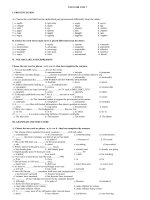
Ferroelectric gating of graphene 7
Bạn đang xem bản rút gọn của tài liệu. Xem và tải ngay bản đầy đủ của tài liệu tại đây (2.43 MB, 10 trang )
Chapter 7
Wafer scale graphene ferroelectric
hybrid devices for low voltage
electronics
In the previous chapters (Chapter 4 and Chapter 6), we discussed the utilization of
ferroelectric polymer (P(VDF-TrFE)) gating for graphene-based novel type of devices
and potential applications. However, the electrostatic doping in graphene provided by
P(VDF-TrFE) is limited by its relatively lower P
r
(8 µC/cm
2
). To enhance the gating
strength further and pursue graphene’s new functionalities, it would be desirable to
utilize ferroelectric inorganic substrates with much higher P
r
as dielectrics.
In this chapter, we report on experiments of CVD single-layer and bilayer graphene
onto functional ferroelectric Pb(Zr
0.3
Ti
0.7
)O
3
(PZT) substrates. Using PZT, we demon-
strate ultra-low-voltage operation of graphene field effect transistors within ±1 V with
maximum doping exceeding 10
13
cm
−2
and on-off ratios larger than 10 times. After
polarizing PZT, the switching of graphene field effect transistors is characterized by
pronounced resistance hysteresis, suitable for ultra-fast non-volatile electronics.
The results discussed in this chapter have been published in Europhysics Letters
[136].
90
91
7.1 Introduction
Ferroelectric inorganic materials are unique both in non-volatile gating [145] and
high polarizability up to 100 µC/cm
2
(6 × 10
14
cm
−2
in charge density) [146], 60
times larger than SiO
2
. With such high gating strength, it is possible to heavily
dope graphene beyond the linear band dispersion regime (∼ 1 eV) and reach the
van Hove singularities [11]. Such high doping, which in contrast to electrolyte gat-
ing [147] is gate-tunable even at liquid helium temperature, may also be of great
importance for verifying the recent theoretical prediction of strong electron-phonon
interactions and high-temperature superconductivity in graphane and related mate-
rials [148]. For graphene electronics, this level of gating strength may enable the
opening of a sizeable non-volatile bandgap up to ∼ 300 meV [41] in bilayer graphene
field effect transistors[22, 149]. This is critical not only for achieving high current on-
off ratio > 10
4
for logic operations but also for improving ∆R/R for memory device
applications. Equally imp ortant, it can significantly reduce the switching voltage to
below 1 V while exceeding the highest doping by SiO
2
gating (10
13
cm
−2
) [63].
Here, we demonstrate the device operation of Cu-CVD single-layer and bilayer
graphene field effect transistors on ferroelectric Pb(Zr
0.3
Ti
0.7
)O
3
(PZT) substrates.
Transistor and non-volatile memory operations have been realized by controlling PZT
polarization magnitude. The ultra-high κ of PZT in the linear dielectric regime allows
graphene field effect transistors to be switched on and off within ±1 V with maximum
doping exceeding 10
13
cm
−2
. After polarizing PZT, the switching of graphene field
effect transistors are characterized by a pronounced resistance hysteresis, ideal for
ultra-fast non-volatile memory.
92
7.2 Results and Discussions
Large-scale graphene used in this study was synthesized by the CVD method on pure
copper foils [44, 50]. By controlling the post-growth annealing time, graphene with
high bilayer coverage of up to 40%, ideal for comparing the performance of both
systems, are synthesized. Subsequently, CVD graphene was transferred to 360 nm
PZT, using the method introduced by Li et al. [150, 151]. Standard e-beam patterning
and metallization was used to fabricate 3 micron size graphene ferroelectric graphene
field effect transistors (GFeFETs). The GFeFETs were then electrically characterized
from room temperature (RT) to 3 K in vacuum in a four-contact configuration using
lock-in amplifiers.
Figure. 7.1a shows the surface morphology of our PZT thin films measured by
atomic force microscopy (AFM). PZT has periodic thickness variations of ∼ 30 nm
at a typical width of 35 µm. These are easily seen as red and green stripes in op-
tical microscopy (Inset of Fig. 7.1d). Cu-CVD graphene transferred on PZT shows
selective enhancement in Raman 2D intensity due to multiple reflection interference
[152, 153]. Raman also indicates significant substrate-induced strain in Cu-CVD
graphene on PZT. As shown in Fig. 7.1e, G peaks of Cu-CVD graphene on PZT
show a noticeable red shift of ∼ 10 cm
−1
and broadening of full width at half max-
imum (FWHM), compared to CVD graphene on SiO
2
. Using the G red shift, we
estimate the PZT-induced strain to be ∼ 0.2% [154]. This implies that Cu-CVD
graphene adapts to the polycrystalline surface of PZT after transfer, which may pro-
vide a lithography free approach for substrate engineering of local strain in graphene
[40]. Note that by reducing the thickness of PZT to 120 nm, SLG and BLG are both
optically and Raman distinguishable. However, thin PZT films usually have much
93
Figure 7.1: (a) AFM of 360 nm PZT thin film. (b) AFM cross-section of PZT
surface. (c) Optical image of high bilayer coverage graphene on SiO
2
. The same
batch graphene is transferred on PZT. (d) Raman spectra of Cu-CVD graphene on
PZT, showing multiple reflection interference induced enhancement in 2D intensity.
(e) FWHM and peak positions of Raman G peaks of Cu-CVD graphene on PZT and
SiO
2
, showing significant substrate-induced strain on PZT. (f) and (g) QHE of CVD
GFeFETs on PZT, showing the SLG/BLG quantization plateaux of (N + 1/2)4e
2
/h
and 4Ne
2
/h respectively. The pronounced hysteresis in both ρ
xx
and σ
xy
is introduced
by the ferroelectric gating.
94
Figure 7.2: (a) Cu-CVD GFeFET arrays on PZT. Inset: Schematic of an individual
Hall bar device. Scale bar: 2 µm. (b) RT R vs V
BG
of a GFeFET in the linear
dielectric regime of PZT. Typical mobility is ∼ 2000 cm
2
V
−1
s
−1
. (c) Linear doping vs
V
BG
relation in the linear regime with a doping coefficient of α = 6.1 × 10
12
cm
−2
V
−1
and κ = 400. (d) RT polarization measurements of PZT thin film in the linear
dielectric regime using a GFeFET as the top electrode.
larger leakage currents. In this study, we use quantum Hall effect measurements to
determine the layer number of graphene. Typical QHE for single-layer and bilayer
CVD GFeFET on PZT is shown in Fig. 7.1f and Fig. 7.1g resp ectively. The char-
acteristic quantization sequences of (N + 1/2)4e
2
/h for SLG and 4Ne
2
/h for BLG
demonstrate the high quality of our Cu-CVD graphene.
In Fig. 7.2a, we show a wafer-scale array of Cu-CVD GFeFETs on PZT. Fig. 7.2b
shows the typical resistance vs gate voltage characteristics (R vs V
BG
) of GFeFETs
without polarizing the PZT thin film by limiting V
BG
below 1.1 V. In this linear
dielectric regime, GFeFETs exhibit high on/off ratios exceeding 10 times with negli-
gible R vs V
BG
hysteresis at ultra-low operating voltages previously known only from
95
electrolyte gated samples. Hall measurements yield a linear doping vs V
BG
relation of
n = αV
BG
, with α = 6.1×10
12
cm
−2
V
−1
(Fig. 7.2c). This doping coefficient translates
into a κ as high as 400 using the electrical displacement continuity equation at the
graphene/PZT interface [66, 84]. The high doping coefficient and κ are further con-
firmed by polarization measurement on the PZT thin film using the GFeFET as the
top electrode (Fig. 7.2d). Compared to the previous literature report of GFeFETs on
400 nm epitaxial Pb(Zr
0.2
Ti
0.8
)O
3
using multilayer graphene [155, 156], the doping
coefficient in our CVD GFeFETs on PZT is almost 6 times higher. The difference in
κ and doping coefficient is most likely due to the different compositions of the PZT
thin films. Indeed, by substitutional doping of Pb by Lanthanum (La) and by fine
tuning the ratio b etween Zr and Ti, we have observed a much enhanced κ of ∼ 2000
(not shown). Note that GFeFETs on PZT have a very broad transition area near the
Dirac point, manifested by significant deviation from linear n vs V
BG
relation below
3 × 10
12
cm
−2
(Fig. 7.2b and 7.2c). This indicates the electron-hole puddle intensity
of graphene on PZT is an order-of-magnitude higher than graphene on SiO
2
. The
strong charge inhomogeneity in graphene on PZT is likely due to the unpolarized
surface dipoles of ferroelectric thin films.
Beyond the linear regime (V
BG
> 1.1 V), the polarization of PZT leads to a pro-
nounced hysteresis in R vs V
BG
(Fig. 7.3a). The increasing P
r
not only increases
the separation between the two resistance peaks, but also decreases the resistance
minimum. This is because that in the polarized regime, dipole charges on ferroelec-
tric are aligned along the same direction and flip as a single domain. Such domain
flipping of dipole charges effectively mimics the clustering of organic residues, which
are expected to reduce long-range scattering in CVD graphene [157]. Indeed, after
96
fully polarizing the PZT thin film, there is a factor of ∼ 2 enhancement in mobil-
ity to ∼ 4000 cm
2
V
−1
s
−1
. The resistance hysteresis in Fig. 7.3a can be utilized for
non-volatile memory and data storage applications [66]. Compared to the ferroelec-
tric polymer used in Ref. [66], PZT allows for a significantly lower device operating
voltage (< 1 V), much faster switching speed (< ns), and ultra-high endurance (10
10
cycles). In Fig. 7.3b, we show the fatigue test (±10 V) of PZT thin films using a
GFeFET as the top electrode. The nearly constant P
r
indicates that graphene can
effectively stop metal in the top layer migrating into PZT, which is the main degrada-
tion mechanism of inorganic ferroelectric. The slight degradation during the first 10k
cycles is likely due to the low work function aluminum, which may contact exposed
PZT surface during the wire bonding process.
Last but not least, we discuss the observation of anti-hysteresis resistance in PZT
gated GFET devices which has an opposite direction from the polarization direction
of the PZT as illustrated by arrows on Fig. 7.3a and Fig. 7.3c. Currently, the
exact origin of this anti-hysteresis resistance loop has yet to be clarified and there
are several possible mechanisms can lead to such observation; one is due to charge
trapping in the interface states [158], the second one is polarization screening from
water molecules between graphene and PZT [156], and the last one is the partially
suspended graphene due to the high surface roughness of PZT substrate. In the
following, we discuss these points separately.
To investigate the effect of graphene on the interface of PZT, Song et al. com-
pared the capacitance-voltage characteristics (C-V) of a ferroelectric capacitor with
(Pt/G/PZT/Pt) and without graphene (Pt/PZT/Pt) [158]. The position and value
of the normalized capacitance maxima drastically changes, which can either caused
97
by the work function difference of the two metal plates or charges at the interface
states. By assuming that the work function difference is negligible, they suggested
that it is possible to explain one possible mechanism for the anti-hysteresis effect
[158].
In contrary, Hong et al. proposed that the adsorbed water molecules are the
original source for such observations [156]. Utilizing the wet transferring method,
there is a high possibility that water molecules would be involved at the interface of
CVD graphene and PZT substrate. Consequently, the water molecules can serve as
charged adsorbates to screen the polarization of PZT prior to the graphene. Since
water is known to have two metastable forms when chemisorbed on the surface of
transition metal oxides. It can either maintains its molecular form or dissociates into
H
+
and OH
−
. Thus, such dynamic dissociation/recombination of water molecules
chemisorbed at the interface of graphene/PZT can lead to the anti-hysteresis resis-
tance change [156].
The high surface roughness of PZT thin film is another possible reasons for this
anti-hysteresis resistance loop. This is because the graphene working channels can
be partially suspended from the substrate and contribute to an equivalent capacitor
(C
vacuum
) in series with the C
P ZT
from PZT dielectric, as shown in Fig. 7.3d. When
sweeping V
BG
from zero to V
max
, PZT in the normal regimes will reverse the dipole
polarization from negative to positive. In contrast, PZT in the suspended regimes
will retain nearly the same polarization, since V
BG
is mainly dropped on the vacuum
capacitor (C
vacuum
/C
P ZT
< 0.1). Once reaching V
max
, V
BG
is swept back to zero.
However, the potential on C
vacuum
remains close to V
max
because the discharging of
C
vacuum
is slower than the V
BG
sweeping. Consequently, an electric field opposite to
98
PZT substrate
(a)
(b)
PZT
Graphene
Pt
V
BG
=0
V
BG
C
PZT
C
vacuum
V
2
PZT
Graphene
Pt
V
BG
V
BG
C
PZT
C
vacuum
V
2
~ V
BG
E
PZT
Graphene
Pt
V
BG
V
BG
C
PZT
C
vacuum
V
2
~ V
max
E
PZT
Graphene
Pt
V
BG
=0
V
BG
C
PZT
C
vacuum
V
2
''
i. 0V ii. 0V to V
max
iii. V to 0V iv. 0V
max
(c)
(d)
Figure 7.3: (a) The evolution of R vs V
BG
hysteresis as a function of maximum V
BG
for PZT substrate. (b) Fatigue test of PZT films using CVD GFeFET as the top
electrodes. (c) Doping hysteresis deduced from Hall measurements and the expected
ferroelectric doping hysteresis deduced from the electrical displacement continuity
equation at the graphene/ferroelectric interface. Hall-deduced hysteresis not only has
a counter clockwise direction, opposite to the clockwise ferroelectric doping hysteresis,
but also has much larger coercive field. (d) Ferroelectric dipole flipping in normal and
suspended regimes. The orange arrows represent the polarization directions. Bigger
arrow size represents larger spontaneous polarization.
the applied gate voltage will be created and reverse the dipole polarization in the
suspended areas. Thus, the polarization reversals of PZT in the suspended regimes
only happens during the discharging of C
vacuum
, which explains the counter clockwise
Hall-deduced doping hysteresis.
99
7.3 Conclusion
In conclusion, we demonstrated the wafer-scale patterning and device operations of
Cu-CVD GFET devices on PZT substrates, integrating both transistor and non-
volatile memory functionalities on the same chip by controlling the PZT polarization
magnitude. In the linear regime of PZT, we show ultra-low voltage operations of
GFeFETs within ±1 V, which can be used as controlling transistors for addressing and
reading/writing of memory unit cells. After p olarizing PZT, the hysteretic switching
of GFeFETs are ideal for ultra-fast non-volatile data storage. To fully utilize the
switching speed of PZT, a constant doping is required to electrostatically “biased” the
symmetrical ferroelectric doping hysteresis and create two distinct resistance states
[84]. This can be realized by non-destructive charge-transfer doping via the deposition
of low work function materials on the top surface of GFeFETs [159].