AN0212 smart sensor CAN node using the MCP2515 and PIC16F876
Bạn đang xem bản rút gọn của tài liệu. Xem và tải ngay bản đầy đủ của tài liệu tại đây (418.66 KB, 84 trang )
AN212
Smart Sensor CAN Node Using the MCP2515 and PIC16F876
Author:
Mike Stanczyk
Diversified Engineering, Inc.
INTRODUCTION
Advances in data communications have created
efficient methods for several devices to communicate
over a minimum number of system wires. The
Controller Area Network (CAN) is one of these
methods. CAN sends and receives messages over a
two-wire CAN bus. The nodes broadcast their
individual messages over the CAN bus. Meanwhile, the
receivers are set up to accept the message and
anticipate an Acknowledgment (ACK) signal, indicating
the receipt of a non-corrupted message. The protocol
of the CAN has two states and the bits are either
dominant (logic ‘0’) or recessive (logic ‘1’). Nodes may
attempt to transmit a message at the same time. To
ensure that collisions do not reduce the throughput of
the bus, there is an arbitration scheme. In this scheme,
a node will continue to transmit until a dominant bit is
detected, while that node is expecting a recessive bit
(in the ID field) on the CAN bus. The node(s) that lost
arbitration will automatically terminate their transmission and switch to Receive mode. After the CAN bus
enters an Idle state, these nodes attempt to retransmit.
If the node did not lose arbitration, it completes its
transmission. (For additional information on the CAN
protocol, refer to AN713, “Controller Area Network
(CAN) Basics”, DS00713.)
MODULE OVERVIEW
The module hardware can be divided into two
components. These are:
• CAN-NET Node Board
• CAN-NET Analog Input Board
These boards can be purchased from Diversified
Engineering by ordering the CAN-NET Analog Input
Node Kit. The CAN-NET Analog Input Board also
requires that some of the options be installed by the
customer. Two additional components are: a 14.5-PSI
Pressure Transducer and an LED. Table 1 gives the
part numbers for these components.
TABLE 1:
Manufacturer
COMPONENT PART
NUMBERS
Part
Number
Component
Diversified
Engineering
CAN-NET
905190
Analog Input Node Kit
Motorola®
Pressure Transducer
MPX2010DP
This module has several key features. These include:
•
•
•
•
•
High-Speed SPI Interface
MPLAB® ICD Debugging Tool
Low-Power CMOS Technology
PWM Output for Driving a Lamp
Supports SPI modes 0,0 and 1,1
The bus configuration operates by the multi-master
principle, and allows several Node Boards to connect
directly to the bus. If one Node Board fails in the
system, the other Node Boards are not affected. The
probability of the entire network failing is extremely low
compared to ring type networks. Ring type networks
have a high probability failure rate, due to the fact that
if one node malfunctions, the entire network becomes
inoperable. The CAN controller seeks to solve this
problem.
MCP2515 CAN Controller Benefits
• Monitors Several Devices
• Individual Node Programming
• Replaces a Large Wiring Harness
2010 Microchip Technology Inc.
DS00212C-page 1
AN212
CAN-NET Node Board
CAN-NET Analog Input Board
The CAN-NET Node Board consists of hardware
devices that are used in conjunction with software programming techniques to achieve an optimal Controller
Area Network. The versatility of the CAN controller
enables a wide variety of applications to be created,
based on the concept of this particular design.
The MCP3201 ADC accepts input signals from the
pressure sensor, utilizing a differential amplifier configuration. The MCP602 amplifier uses single-supply
CMOS operational amplifier (op amp) technology.
HARDWARE OVERVIEW
The MCP2515 CAN controller is the heart of the CAN
interface. It handles all of the transmitting and receiving
of message packets that contain useful information for
other nodes on the network via the CAN bus. The
MCP2515 CAN controller is also designed to interface
with the Serial Peripheral Interface (SPI) port. The SPI
port is available on the PIC16F876 microcontroller, and
the MCP3201 Analog-to-Digital Converter (ADC).
This section describes the CAN-NET Node Board
hardware and how the CAN functions in the Node Board
system. Schematics can be found in Appendix A:
“Schematics”.
MCP2515 CAN Controller
The high-level design of this system is shown in
Figure 1. The concept is to enable the MCP2515 CAN
controller, the PIC16F876 microcontroller and the
MCP3201 ADC to efficiently communicate among each
other, utilizing the SPI. The MCP2515 handles the
lower level protocols.
The PIC16F876 microcontroller stores the program in
memory and reads the DIP switch settings for sending
and receiving messages. It controls the PWM output
and enables the MPLAB® ICD to be used as a
debugging tool.
FIGURE 1:
BLOCK DIAGRAM OF THE CAN NODE BOARD
+5V
•
•
•
•
•
•
•
•
•
PWM
Output
LED
MCP2515
MCP2551
SPI
CAN
Driver
CAN
Controller
4
Microcontroller
MPLAB®
ICD
SPI
CAN bus
PIC16F876
SPI
ADC
Filter
MCP3201
MCP602
Amplifier
Pressure
Sensor
MCP602
DS00212C-page 2
MPX2100AP
2010 Microchip Technology Inc.
AN212
The PIC16F876 microcontroller stores the program in
memory and constantly polls the MCP3201 ADC, along
with the reference A/D.
In the main loop of the program, a variable is toggled.
When the value of the variable is a logic ‘0’, the PIC®
device reads the pressure sensor, and when the value
of the variable is a logic ‘1’, the PIC® device reads the
reference A/D. The microcontroller also reads the
settings of the input switches.
FIGURE 2:
The first two (of four) switches tell the microcontroller
which message the node is allowed to receive. The last
two (of four) switches tell the microcontroller the
transmit address of the node. The configuration, shown
in Figure 3, illustrates three Node Boards on a CAN
bus, and they are set to transmit and receive certain
messages.
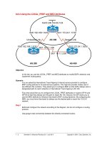
THREE NODE BOARDS CONNECTED TO THE CAN BUS
Rx
Tx
10
01
PWM
NODE BOARD 1
Rx
Tx
11
10
PWM
NODE BOARD 2
Rx
Tx
01
11
PWM
NODE BOARD 3
CAN bus
2010 Microchip Technology Inc.
DS00212C-page 3
AN212
In this case, each node transmits its own pressure
sensor value and each node is set to receive a value of
the pressure sensor from a different node. The
identification for each Node Board is ‘01’, ‘10’ and ‘11’.
These settings are transmit and receive identifiers.
Node Board 1 is set to receive the pressure sensor
value from Node Board 2. Node Board 2 is set to
receive the pressure sensor value from Node Board 3,
and Node Board 3 is set to receive the pressure sensor
value from Node Board 1. The pressure sensor value
of each Node Board is directly proportional to the PWM
output of the corresponding microcontroller.
Figure 3 shows a differential amplifier circuit. The input
to this amplifier ranges from 0 to 5 volts and is useful
for pressure applications. The pressure can be referred
to as “zero pressure”. The normalized pressure setting
consists of negative pressure (when there is intake)
and positive pressure (when there is outtake). The
pressure sensor produces a negative voltage when
there is negative pressure, and a positive voltage when
there is positive pressure. The reference for the differential amplifier is 2.5 volts. Above 2.5 volts, it indicates
a positive pressure. Below 2.5 volts, it indicates a
negative pressure. The CAN-NET Node Board with the
Analog I/O Board is designed specifically for pressure,
but can easily be altered to do both.
The CAN driver chip converts the input and output to
the CAN bus voltages, ranging from 0 to 5 volts with a
shift of ±12V.
Hardware Tools
The MCP3201 is a 12-bit ADC with on-board sample
and hold circuitry.
The MPLAB ICD is a tool which enhances the code
development and hardware debugging process. The
debugger uses a PIC16F877 device and operates in
“real time”. This low-cost tool saves engineering time
(“expenses”) by allowing the application program and
circuit to be evaluated, and enhanced in real time. The
ICD interface also allows the PIC16F87X devices to be
programmed after the board has been manufactured.
This allows software changes or updates to be
programmed into the device. The ICD uses the RB6 and
RB7 pins of the PIC16F87X for this. For that reason,
these pins are not used for any other purpose in this
system. For additional information on In-Circuit Serial
Programming, please refer to Microchip’s “In-Circuit
Serial Programming™ (ICSP™) Guide”, (DS30277).
The input to the device comes from a differential
amplifier circuit, which communicates over the serial
interface, using the SPI protocol. The MCP602 op amp
is used to design a suitable differential amplifier.
The gain of the amplifier is determined by the following
equation:
EQUATION 1: AMPLIFIER GAIN
R14
R13
Gain = 1 + ---------- + 2 ----------R13
RP1
FIGURE 3:
DIFFERENTIAL AMPLIFIER CIRCUIT
+5V
1
2
3
4
5
+5V
PSI
MPX2010DP
3
1.45PSI
V
2
RC2
J4
RP1
4
R14
R12
GND
1
R11
RA0
(REF_2.5V)
2
3
U4
MCP602
1
R13
6
5
Component
Value
7
R15
Tolerance
R11
30.1 k
1%
R12
10.0 k
1%
R13
10.0 k
1%
R14
30.1 k
1%
R15
1.0 K
1%
RP1
0.0 to 50.0 k
N.A.
DS00212C-page 4
U4
MCP602
2010 Microchip Technology Inc.
AN212
SOFTWARE OVERVIEW
Programming Style
The code for the Node Board is written in the PIC®
device instruction set to be assembled using
Microchip’s MPLAB environment. There is a significant
use of macros to make the code more readable and
less error prone. The macros are defined in three files:
1. Near the top of the main file
2. canlib.asm (file contains the CAN macros)
3. macros16.inc
General ID Structure
The ID structure used by the Node Boards is
determined by the settings on the DIP switches on
power-up or after a Reset. Changing the DIP switches
while running, has no effect on the ID structure.
Receive ID Structure
The Node Board uses the following setting in Table 2
for receiving:
TABLE 2:
If an unfamiliar instruction is found, it is probably made
up of a set of familiar instructions in one of the macros.
The macros in the macros16.inc file are used
extensively in writing code for the PIC® microcontroller
family, because they increase readability and greatly
reduce programming errors.
RECEIVING SETTINGS FOR
THE NODE BOARD
Register
Value
RxMask0
0xFFF
RxMask1
0xFFE
RxFilter0
0xFFF
RxFilter1
0xFFF
Common Code
RxFilter2
0xn00 (1)
The Node Board uses common software files to
maximize the program’s efficiency. The routines that
enable communication with the MCP2515 CAN chip
are in the file canli.asm and the definitions of the
MCP2515 registers are in mcp2515.inc. The
common macros are in macros16.inc.
RxFilter3
0xn10
RxFilter4
0xFFF
RxFilter5
0xFFF
SPI Communications
Communications from a device on the node (such as a
microcontroller) to the MCP2515 are through the SPI
bus. The PIC® device used on the Node Board fully
supports the SPI in the Master mode. Command
strings are sent and received using a single software
buffer. To send a string, the software buffer, called
pSPIBufBase, is loaded with the bytes to send and
the SPI interrupt is turned on. The interrupt handler
exchanges bytes with the MCP2515. The bytes
received from the MCP2515 replace the bytes that
were sent from the software buffer, so that after the
string has been sent, the buffer will contain the bytes
received from the MCP2515. All communications with
the MCP2515 are handled in this manner and is
encapsulated in the routines in the canlib.asm.
2010 Microchip Technology Inc.
Note 1:
This value is the Base Receive ID for
receiving. The DIP #1 and DIP #2 settings
are used to determine this value.
The DIP settings for receiving are shown in Table 3.
TABLE 3:
DIP SWITCH ID SETTINGS FOR
RECEIVING
DIP #1
DIP #2
ID
0
0
0x000
0
1
0x100
1
0
0x200
1
1
0x300
A message received for RxFilter2 (Base Receive ID) is
assumed to be a two-byte integer that contains a 12-bit
value, between 0 and 4095. The 12-bit data is used to
generate a PWM output, where a ‘0’ generates a 0%
duty cycle and 0xFFF generates a 100% duty cycle.
DS00212C-page 5
AN212
Transmit ID Structure
The Node Board transmits a CAN message every
131 ms. A message contains two data bytes that
represent a 12-bit value with the Least Significant Byte
(LSB) sent first.
The pressure switch is assigned to the Base Transmit
ID and is measured and transmitted with that ID every
393 ms, as a two-byte integer in the range of 0 to 4095.
Note that the A/D measurement is 8 bits, which is then
shifted by 4 bits before transmission; hence, its actual
range is 0x0000 to 0x0FF0.
Each data source has its own unique Base Transmit ID
obtained from the settings of DIP #3 and DIP #4. These
settings are shown in Table 4.
TABLE 4:
DIP SWITCH ID SETTINGS FOR
TRANSMITTING
DIP #3
DIP #4
0
0
All transmissions are disabled
0
1
0x100
1
0
0x200
1
1
0x300
TABLE 5:
ID
The MCP2515 CAN controller has a 125-Kbit rate and
the polling method is used. The use of interrupts would
be easier in the system, but polling allows the interrupt
pins to remain free for other potential functions in the
system.
There are three methods for transmitting information:
1.
2.
3.
Responding to an external event (event driven).
Sending messages at regular intervals (timed
transmission). The time of the event may be
unknown.
A combination of the first two. The receiver can
expect messages at a maximum known interval.
The flowcharts for the operation of the source code are
shown in Figure 4 through Figure 24. The subroutines
contain the actual name and the function it performs
within the flowchart, so that it can be easily referenced
with the source code. Table 5 gives the function names
used and a brief description of the function. In the
electronic version of this document, clicking of the
function name will ink you to the page for that function.
SOFTWARE FUNCTION DESCRIPTIONS
Function Name
Main
Figure
Number
Function Description
This is the main loop of the program.
Figure 4
Hardstart
Does a full initialization of the system.
Figure 5
Init
Initializes the PIC16F87X registers.
Figure 6
InitSPIPort
Initializes the PIC16F87X SPI port.
Figure 7
Init2515
Initializes the MCP2515 registers.
Figure 8
Read3201
Reads the specified register in the MCP3201 (A/D Converter).
Figure 9
ReadA2D
Reads the specified register in the MCP3201 (A/D Converter).
Figure 10
WaitANDeqZ
Waits for pending messages.
Figure 11
CheckCANMsg
Checks for messages in the receive buffer.
Figure 12
ParseCAN
Set up messages for the PWM output.
Figure 13
Reset2515
Resets the MCP2515.
Figure 14
BitMod2515
Modifies the value of a specified bit in the MCP2515.
Figure 15
Wrt2515Reg
Writes the specified register in the MCP2515 (CAN interface).
Figure 16
SetNormalMode
Sets the MCP2515 to normal operating mode.
Figure 17
Rd2515Reg
Reads the specified register in the MCP2515 (CAN interface).
Figure 18
OutputPWM
Loads the PWM Duty Cycle registers with the values in the
specified registers.
Figure 19
InitSPIBuf
Initializes SPI buffer for transaction.
Figure 20
LoadSPIByte
Loads the value in the W register into the SPI buffer.
Figure 21
ExchangeSPI
Initiates the SPI transaction.
Figure 22
WaitSPIExchange
Waits for the SPI transaction to be completed.
Figure 23
LoadSPIZeros
Clears the value in the SPI buffer.
Figure 24
DS00212C-page 6
2010 Microchip Technology Inc.
AN212
CONCLUSION
The MCP2515 offers a simple method to interface a
CAN network in order to maximize the transmitting and
receiving of data via the CAN bus. This efficient method
allows a wide variety of I/O devices to be connected to
the network using a Node Board. An advantage in
utilizing this type of system is the ability to monitor several Node Boards at any given time. If an error occurs,
it is detected and retransmitted over the bus line until
the receiver Acknowledges the message. Another
advantage is that several Node Boards can work from
one bus line, rather than using a large wiring harness
that connects to a main control panel. Our design demonstrated a way to implement a simple input pressure
switch connected to a Node Board, along with a visual
light source to display the value in terms of brightness.
By this example, several uses for different types of
inputs and outputs can be implemented by using the
basic techniques from this design.
2010 Microchip Technology Inc.
CONTACTING DIVERSIFIED
ENGINEERING
Additional information and CAN related products may
be acquired from Diversified Engineering, Inc. You may
contact them by either calling:
(202) 726-7676
or by visiting their web site:
www.diveng.com
DS00212C-page 7
AN212
FIGURE 4:
MAIN PROGRAM LOOP (Main)
Main
Initialize System from POR
(Hardstart)
Message
Type = 1?
No
No (= 0)
Yes
Transmit
CAN
Message?
Read A/D Reference
(ReadA2D)
Read A/D Pressure
(Read3201)
Yes
Reload Counter
Use TX DIP Address
for Transmission
Transmission
Turned Off?
No
Yes
Check CAN Message
(CheckCANMsg)
No
Assemble new Message
Using New Source and ID
Wait for Pending Messages
(WaitANDeqZ)
Output CAN
Message
New
CAN Message
Received?
Yes
Parse the Message
(CheckCANMsg)
DS00212C-page 8
2010 Microchip Technology Inc.
AN212
FIGURE 5:
HARDSTART (Hardstart)
Hardstart
Initialize PICmicro® MCU
(Init)
Deselect Devices on SPI bus
Read the DIP Switches
Create ID for Transmit
and Receive
Initialize PICmicro MCU SPI Port
(InitSPIPort)
Delay 28 msec (for MCP2515)
Initialize MCP2515 Registers
(Init2515)
Return
2010 Microchip Technology Inc.
DS00212C-page 9
AN212
FIGURE 6:
INITIALIZE PICmicro® MCU (Init)
Init
Clear Peripheral Interrupt bits
Clear GPR Registers in Bank 0
Clear GPR Registers in Bank 1
Turn on A/D Conversion
Initialize Ports (A, B and C)
Configure Timer
Initialize PWM
Initialize Ports (A, B and C)
Enable Peripherals Only
Return
DS00212C-page 10
2010 Microchip Technology Inc.
AN212
FIGURE 7:
SETUP SPI PORT (InitSPIPort)
InitSPIPort
Disable SPI Module
Configure as Master Mode SPI
Enable SPI
Clear SPI Interrupt Flag (SSPIF)
SPP Enable Bank 1
Return
2010 Microchip Technology Inc.
DS00212C-page 11
AN212
FIGURE 8:
SETUP MCP2515 REGISTERS (Init2515)
Init2515
Reset MCP2515 Registers
(Reset2515)
Set Clock Output Prescaler to
Divide by 4
Write Data in Register Using Mask
(BitMod2515)
Set Physical Layer Configuration
Configure Receive Buffer 0
Mask and Filters
Configure Receive Buffer 1
Mask and Filters
Configure Filter 2 to Match
ID from DIP Switch Settings
Configure Filter 3 to Match
ID from DIP Switch Settings
Disable MCP2515 Interrupts
Write W Register to MCP2515 Register
(Wrt2515Reg)
Set Normal Mode
(SetNormalMode)
Return
DS00212C-page 12
2010 Microchip Technology Inc.
AN212
FIGURE 9:
READ A/D PRESSURE (Read3201)
Read3201
Initialize SPI Buffer
(InitSPIBuf)
Clear the SPI Buffer
(LoadSPIZeros)
Initiate SPI Transaction
Load First Byte to Begin Exchange
Wait for SPI Completion
(WaitSPIExchange)
Shift Byte Right One bit
(to remove extra bit)
Clear Upper 4 bits
Return
2010 Microchip Technology Inc.
DS00212C-page 13
AN212
FIGURE 10:
READ A/D REFERENCE (ReadA2D)
ReadA2D
Configure A/D Input Channel
Turn on A/D
Start A/D Conversion
No
A/D
Conversion
Complete?
Yes
Convert Result to 12 bits
Return
DS00212C-page 14
2010 Microchip Technology Inc.
AN212
FIGURE 11:
WAIT FOR PENDING MESSAGES (WaitANDeqZ)
WaitANDeqZ
Put Address in Register
Save Address in Register
Read MCP2515 Register at Address Pointed to in W Register
(Rd2515Reg)
No
Address
Match?
Yes
Return
2010 Microchip Technology Inc.
DS00212C-page 15
AN212
FIGURE 12:
CHECK CAN MESSAGE (CheckCANMsg)
CheckCANMsg
New
CAN Message
Received?
No
Yes
No
Message
Pending?
Return
Calculate Receive Buffer Location
Yes
Get Data Byte
Get ID out of Message Source
Read MCP2515 Register at
Address Pointed to in W Register
(Rd2515Reg)
Get Number of Bytes of Data
Save Data
No
More Data?
Calculate Destination Buffer Location
Yes
Store Data in Buffer
Clear Receive Buffer
Signal Data Pending
Return
DS00212C-page 16
2010 Microchip Technology Inc.
AN212
FIGURE 13:
PARSE THE MESSAGE (ParseCAN)
ParseCAN
Received
ID Base?
No
Yes
Extract Data (12 bits)
from Message
No
Received
ID Base + 1?
Yes
Convert Data to 8-Bit PWM Output
(by masking lower 4 bits)
Extract Data (12 bits)
from Message
Output PWM
(OutputPWM)
Data
0x800?
No
Yes
Turn RX LED on
Turn RX LED off
Return
2010 Microchip Technology Inc.
DS00212C-page 17
AN212
FIGURE 14:
RESET MCP2515 REGISTERS (Reset2515)
Reset2515
Initialize SPI Buffer
(InitSPIBuf)
Reset MCP2515
Load W Register into SPI Buffer
(LoadSPIByte)
Initialize SPI Buffer
(InitSPIBuf)
Initiate SPI Transaction
(ExchangeSPI)
Wait for SPI Completion
(WaitSPIExchange)
Return
DS00212C-page 18
2010 Microchip Technology Inc.
AN212
FIGURE 15:
WRITE DATA IN REGISTER USING MASK (BitMod2515)
BitMod2515
Save Message Address
Initialize SPI Buffer
(InitSPIBuf)
Send MCP2515
Modify Register Command
Load W Register into SPI Buffer
(LoadSPIByte)
Load Address into
W Register
Load W Register into SPI Buffer
(LoadSPIByte)
Load Mask into
W Register
Load W Register into SPI Buffer
(LoadSPIByte)
Load Data into
W Register
Load W Register into SPI Buffer
(LoadSPIByte)
Initiate SPI Transaction
(ExchangeSPI)
Wait for SPI Completion
(WaitSPIExchange)
Return
2010 Microchip Technology Inc.
DS00212C-page 19
AN212
FIGURE 16:
WRITE BYTE IN MCP2515 REGISTER IN W (Wrt2515Reg)
Wrt2515Reg
Save Message Address
Initialize SPI Buffer
(InitSPIBuf)
Send MCP2515
Write Register Command
Load W Register into SPI Buffer
(LoadSPIByte)
Load Address into
W Register
Load W Register into SPI Buffer
(LoadSPIByte)
Load Data into
W Register
Load W Register into SPI Buffer
(LoadSPIByte)
Initiate SPI Transaction
(ExchangeSPI)
Wait for SPI Completion
(WaitSPIExchange)
Return
DS00212C-page 20
2010 Microchip Technology Inc.
AN212
FIGURE 17:
SET NORMAL MODE (SetNormalMode)
SetNormalMode
Configure Mask and
Data Addresses
Write Data in CANCNTL Register
(BitMod2515)
Read MCP2515 Register at Address Pointed to in W Register
(Rd2515Reg)
No
Value
ANDed
0x0E = 0?
Yes
Return
2010 Microchip Technology Inc.
DS00212C-page 21
AN212
FIGURE 18:
READ REGISTER ADDRESS IN W (Rd2515Reg)
Rd2515Reg
Save Message Address
Initialize SPI Buffer
(InitSPIBuf)
Send MCP2515
Read Register Command
Load W Register into SPI Buffer
(LoadSPIByte)
Load Address into
W Register
Load W Register into SPI Buffer
(LoadSPIByte)
Clears the Value in the SPI Buffer
(LoadSPIZeros)
Initiate SPI Transaction
(ExchangeSPI)
Wait for SPI Completion
(WaitSPIExchange)
Return
DS00212C-page 22
2010 Microchip Technology Inc.
AN212
FIGURE 19:
OUTPUT PWM (OutputPWM)
OutputPWM
Extract Data (8 bits)
from Message
Load Data into
PWM Register
Turn on PWM Output
Load Upper 8 bits into
CCPR1 Register
Return
FIGURE 20:
INITIALIZE SPI BUFFER (InitSPIBuf)
InitSPIBuf
Load FSR with Start Address of
SPI Buffer
Return
FIGURE 21:
LOAD BYTE IN W TO SPI BUFFER (LoadSPIByte)
LoadSPIByte
Increment FSR Register
Return
2010 Microchip Technology Inc.
DS00212C-page 23
AN212
FIGURE 22:
INITIATE SPI TRANSACTION (ExchangeSPI)
ExchangeSPI
Get Number of Bytes to Exchange
Bytes 0?
No
Yes
Load Number of Bytes in Buffer
Load Byte to Begin Exchange
Send Byte(s)
Return
FIGURE 23:
WAIT FOR SPI COMPLETION (WaitSPIExchange)
WaitSPIExchange
No
SPI
Communication
Completed
?
Yes
Return
DS00212C-page 24
2010 Microchip Technology Inc.
AN212
FIGURE 24:
LOAD NUMBER OF ZEROS IN W TO SPI BUFFER (LoadSPIZeros)
LoadSPIZeros
W Register
= 0?
Yes
No
Clear Address
Pointed to by FSR
Increment FSR
Add 0xFF to
W Register
No
Return
2010 Microchip Technology Inc.
W Register
= 0?
Yes
DS00212C-page 25