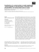
AN1197 using a hardware module to interface 8051 MCUs with SPI serial EEPROMs
Bạn đang xem bản rút gọn của tài liệu. Xem và tải ngay bản đầy đủ của tài liệu tại đây (275.66 KB, 14 trang )
AN1197
Using a Hardware Module to Interface
8051 MCUs with SPI Serial EEPROMs
Author:
Alexandru Valeanu
Microchip Technology Inc.
INTRODUCTION
The 25XXX series serial EEPROMs from Microchip
Technology support a half-duplex protocol that
functions on a master-slave paradigm that is ideally
suited to data stream applications. The bus is
controlled by the microcontroller (master), which
accesses the 25XXX serial EEPROM (slave) via a
simple Serial Peripheral Interface (SPI) compatible
serial bus. Bus signals required are a clock input (SCK)
plus separate data in (SI) and data out (SO) lines.
Access to the 25XXX serial EEPROM is controlled
through a Chip Select (CS) input. Maximum clock
frequencies range from 3 MHz to 20 MHz.
Communication to the 25XXX serial EEPROM can be
paused via the hold pin (HOLD) if the clock line is
shared with other peripherals on the SPI bus. While the
EEPROM is paused, transitions on its inputs are
ignored, with the exception of CS, allowing the MCU to
service higher priority interrupts. After releasing the
HOLD pin, operations resume from the point when the
hold was asserted.
FIGURE 1:
The main features of the 25XXX serial EEPROMs are:
•
•
•
•
•
•
•
•
SPI-compatible serial interface bus
EEPROM densities from 128 bits to 512 Kbits
Bus speed from 3 MHz to 20 MHz
Voltage range from 1.8V to 5.5V
Low power operation
Temperature range from -40°C to +125°C
Over 1,000,000 erase/write cycles
Built-in write protection
This application note is part of a series that provide
source code to help users implement the protocol with
minimal effort.
Figure 1 is the hardware schematic depicting the interface between the Microchip 25XXX series serial
EEPROMs and NXP’s P89LPC952 8051-based MCU.
The schematic shows the connections necessary
between the MCU and the serial EEPROM as tested.
The software was written assuming these connections. The WP and HOLD pins are tied to VCC
through resistors, because the write-protect and hold
features are not used in the examples provided.
CIRCUIT FOR P89LPC952 MCU AND 25XXX SERIAL EEPROM
Vcc (1)
P89LPC952
34
33
32
31
P2.1/MOSI
P2.3/MISO
P2.4/SS
P2.5/SPICLK
25XX256
CS
1
8
Vcc
SO
2
7
HOLD (2)
WP (2)
3
6
SCK
Vss
4
5
SI
Note 1: A decoupling capacitor (typically 0.1 µF) should be used to filter noise on VCC.
Note 2: WP and HOLD pins should have pull-up resistors (2 kΩ to 10 kΩ).
© 2008 Microchip Technology Inc.
DS01197A-page 1
AN1197
FIRMWARE DESCRIPTION
This application note offers designers a set of
examples for the read and write functions for the
Microchip SPI serial EEPROM (byte read/write and
page read/write) using internal hardware parts and a
main routine. The main routine writes a string in the SPI
serial EEPROM, reads it back and compares the two
strings, displaying the results on LEDs on an evaluation
board. Moreover, the main routine sends the results of
the read to the UART to verify the correctness of
operations.
The firmware was written in assembly language for
NXP’s P89LPC952 MCU using the Keil™ µVision3®
IDE and was developed on the Keil MCB950 evaluation
board.
DS01197A-page 2
The code was tested using the 25XX256 serial
EEPROM. The EEPROM features 32K x 8 (256 Kbit)
of memory and 64-byte pages. Oscilloscope screen
shots are shown in this application note. All timings are
based on the internal RC oscillator of the MCU
(7.373 MHz). If a faster clock is used, the code must be
modified to generate the correct delays.
The bus speed in these examples is ~ 1.8 MHz. As
explained in the applicable SPI serial EEPROM data
sheets, the maximum allowed bus speed depends on
the EEPROM’s operating voltage. If desired, the bus
speed may be changed in the initialization routine
(ini_spi) by modifying the SPR1 and SPR0 bits in
the SPI control register (SPCTL) (refer to the section
titled “Initialization”).
© 2008 Microchip Technology Inc.
AN1197
INITIALIZATION
• CPOL = CPHA = 1 (CK = Idle ‘1’, drive on first
edge, sample on second edge)
• SPR1 = SPR0 = 0 (sets the maximum speed
F_spi_ck = main_ck:4 ~ 7.373 MHz:
4 ~ 1.8 MHz)
Initialization consists of three routines: ini_str,
ini_spi and ini_memspi. The ini_str routine
creates the 16-byte string to be written to the serial
EEPROM.
If another speed is desired, the SPR1 and SPR0 bits
must be set to other values.
The ini_spi routine does two things: it prepares the
MCU for communication with the serial EEPROM using
the hardware peripheral, and it initializes the SPCTL
register. The values of the bits in the SPCTL register
are now:
The third routine, ini_memspi, prepares the serial
EEPROM for further writes.
The structure of the initialization operation is as follows:
Write Enable (WREN) + Write STATUS Register (WRSR)
+ WRITE (#NOPROT = 00). The scope plot showing
this operation appears in Figure 2.
• SSIG = SPEN = MSTR = 1 (this enables the SPI
port and sets the block as master)
• DORD = 0 (MSb first)
FIGURE 2:
WRITE TO STATUS REGISTER
CS
0
1
2
3
4
5
6
7
0
1
2
3
4
5
6
7
8
9
10
11
12
13
14
15
1
0
SCK
Command
Command
SI
0
0
0
0
0
1
1
0
0
0
0
0
0
Data to STATUS Register
0
0
1
7
6
5
4
3
2
High-Impedance
SO
© 2008 Microchip Technology Inc.
DS01197A-page 3
AN1197
WRITE ENABLE
Before a write operation to the array can occur, the
MCU must set the Write Enable Latch (WEL). This is
done by issuing a WREN command.
The MCU clears the WEL bit by issuing a Write Disable
(WRDI) command. The WEL bit is also automatically
reset if the serial EEPROM is powered down or if a
write cycle is completed.
Figure 3 shows the WREN and WRITE pair of
commands.
FIGURE 3:
WRITE ENABLE AND WRITE COMMANDS
CS
0
1
2
3
4
5
6
7
0
1
2
3
4
5
6
7
8
9
10
11
SCK
Command
Command
SI
0
0
0
0
0
1
1
0
0
0
0
0
0
Data to S
0
1
0
7
6
5
4
High-Impedance
SO
DS01197A-page 4
© 2008 Microchip Technology Inc.
AN1197
BYTE WRITE
The byte write operation consists of the MCU sending
the WRITE command followed by the word address and
data byte. The word address for the 25XX256 is a
16-bit value, so two bytes must be transmitted for the
entire word address, with the Most Significant Byte sent
first. Note that the WREN command is not illustrated in
this section but is still required to initiate the operation.
Figure 4 shows the sequence MSB address (00), LSB
address (20h) and the first written byte (6Fh).
FIGURE 4:
WRITE COMMAND AND WORD ADDRESS
CS
Twc
0
1
2
3
4
5
6
7
8
9 10 11
21 22 23 24 25 26 27 28 29 30 31
SCK
Command
SI
0
0
0
0
0
16-Bit Address
0
1
0 15 14 13 12
Data Byte
2
1
0
7
6
5
4
3
2
1
0
High-Impedance
SO
© 2008 Microchip Technology Inc.
DS01197A-page 5
AN1197
DATA POLLING (RDSR – CHECK FOR
WIP SET)
When the write operation has ended, the MCU selects
the serial EEPROM and sends the Read STATUS
Register command (RDSR) (‘00000101’ or 0x05), as
shown in Figure 5. The STATUS register is then shifted
out on the Serial Out (SO) pin, resulting in a value of
‘00000011’ or 0x03, also shown in Figure 5. Both the
WEL bit (bit 1) and the WIP bit (bit 0) are set (‘1’),
indicating that the write cycle is in progress.
After the MCU issues a WRITE command, it reads the
STATUS register to check if the internal write cycle has
been initiated. The STATUS register can be
continuously monitored to look for the end of the write
cycle.
FIGURE 5:
DATA POLLING (READ STATUS REGISTER TO CHECK WIP BIT)
CS
0
1
2
3
4
5
6
7
8
9
10
11
12
13
14
15
1
0
SCK
Command
SI
0
0
0
0
0
1
0
1
Data from STATUS Register
High-Impedance
SO
DS01197A-page 6
7
6
5
4
3
2
© 2008 Microchip Technology Inc.
AN1197
DATA POLLING FINISHED (RDSR –
WIP BIT CLEARED)
The firmware remains in a continuous loop and the WIP
status is evaluated until the WIP bit is cleared (‘0’).
Figure 6 shows the RDSR command. This is followed by
a value of 0x00 being shifted out on the SO pin,
indicating that the write cycle has finished and the
serial EEPROM is ready to receive additional
commands. The WEL bit is also cleared at the end of a
write cycle, which serves as additional protection
against unwanted writes.
FIGURE 6:
DATA POLLING FINISHED (RDSR – WIP AND WEL BITS CLEARED)
CS
0
1
2
3
4
5
6
7
8
9
10
11
12
13
14
15
1
0
SCK
Command
SI
0
0
0
0
0
1
0
1
Data from STATUS Register
High-Impedance
SO
© 2008 Microchip Technology Inc.
7
6
5
4
3
2
DS01197A-page 7
AN1197
BYTE READ
The byte read operation can be used to read data from
the serial EEPROM. The MCU transmits the command
byte followed by the word address bytes to the serial
EEPROM.
Figure 7 shows an example of the READ command,
followed by the MSB and LSB address bytes, followed
by the first read byte. After the MCU reads the data
byte, the SO line relaxes and goes to a high impedance
state.
FIGURE 7:
BYTE READ (COMMAND BYTE, WORD ADDRESS AND FIRST READ BYTE)
CS
0
1
2
3
4
5
6
7
8
9 10 11
21 22 23 24 25 26 27 28 29 30 31
SCK
Command
SI
0
0
0
0
0
16-Bit Address
0
1
1 15 14 13 12
2
1
0
Data Out
High-Impedance
SO
DS01197A-page 8
7
6
5
4
3
2
1
0
© 2008 Microchip Technology Inc.
AN1197
PAGE WRITE
addresses that are [integer multiples of the page size]
minus 1. Attempts to write across a page boundary
result in the data being wrapped back to the beginning
of the current page, thus overwriting any data previously stored there.
Page write operations provide a technique for
increasing throughput when writing large blocks of
data. The 25XX256 serial EEPROM features a 64-byte
page. By using the page write feature, up to 1 full page
of data can be written consecutively.
The page write operation is very similar to the byte write
operation. The serial EEPROM automatically increments the internal Address Pointer to the next higher
address with receipt of each byte.
It is important to note that page write operations are
limited to writing bytes within a single physical page,
regardless of the number of bytes actually written.
Physical page boundaries start at addresses that are
integer multiples of the page size, and end at
FIGURE 8:
Figure 8 shows four consecutive data bytes during a
page write operation.
PAGE WRITE (FIRST FOUR CONSECUTIVE DATA BYTES)
CS
0
1
2
3
4
5
6
7
8
9 10 11
21 22 23 24 25 26 27 28 29 30 31
SCK
Command
SI
0
0
0
0
0
16-Bit Address
0 1
0 A15 A14 A13 A12
Data Byte 1
A2 A1 A0 7
6
5
4
3
2
1
0
CS
32 33 34 35 36 37 38 39 40 41 42 43 44 45 46 47
SCK
Data Byte 2
SI
7
6
5
4
© 2008 Microchip Technology Inc.
3
2
Data Byte 3
1
0
7
6
5
4
3
2
Data Byte n (64 max)
1
0
7
6
5
4
3
2
1
0
DS01197A-page 9
AN1197
PAGE READ
Page read operations read a complete string, starting
with the specified address. In contrast to page write
operations described on the previous page, there is no
maximum length for page read. After 64 Kbytes have
been read, the internal address counter rolls over to the
beginning of the array.
Figure 9 depicts the entire sequence of commands
necessary to perform the page read operation. For
clarity, only the first two read bytes are shown.
FIGURE 9:
PAGE READ (FIRST TWO READ BYTES)
CS
0
1
2
3
4
5
6
7
8
9 10 11
21 22 23 24 25 26 27 28 29 30 31
SCK
Command
SI
0
0
0
0
0
16-bit Address
0
1
1 A15 A14 A13 A12
A2 A1 A0
Data Byte 1
High-Impedance
SO
DS01197A-page 10
7
6
5
4
3
2
1
0
© 2008 Microchip Technology Inc.
AN1197
BYTE WRITE VERSUS PAGE WRITE
At first glance, the page write method appears superior
to the byte write method: it’s simpler and faster.
However, a careful analysis shows that the byte write
method has a major advantage over page write owing
to the roll-over phenomenon (see Note).
Note:
Page write operations are limited to writing
bytes within a single physical page,
regardless of the number of bytes actually
being written. Physical page boundaries
start at addresses that are integer
multiples of the page buffer size (or page
size), and they end at addresses that are
integer multiples of [page size-1]. If a
Page Write command attempts to write
across a physical page boundary, the
result is that the data wraps around to the
beginning of the current page (overwriting
data previously stored there) instead of
being written to the next page as might be
expected. It is therefore necessary for the
application software to prevent page write
operations that would attempt to cross a
page boundary.
As a consequence of the roll-over phenomenon, applications that write long strings to the SPI serial
EEPROM risk overlapping the page boundary in the
middle of a string. In such instances, the firmware
should use byte write to avoid this condition. The disadvantage of doing this is the slower speed involved in
writing the entire string: every byte write cycle time is
approximately 5 ms.
© 2008 Microchip Technology Inc.
The following summarizes the differences between the
byte write and page write methods.
Byte Write
• Is slower – It needs a 5 ms write cycle time for
each byte.
• Is more general – It may write a string of any
length.
Page Write
• Is faster – It needs only one write cycle time for
the whole page.
• Care must be taken to observe page boundaries
during page writes.
CONCLUSION
This application note offers designers a set of firmware
routines to access SPI serial EEPROMs using a
hardware peripheral. The code demonstrates byte and
page operations. All routines were written in the
assembly language for an 8051-based MCU.
The code was developed on the Keil MCB950
evaluation board using the schematic shown in
Figure 1. It was tested using the NXP P89LPC952
MCU and debugged using the Keil µVision3 IDE.
DS01197A-page 11
AN1197
NOTES:
DS01197A-page 12
© 2008 Microchip Technology Inc.
Note the following details of the code protection feature on Microchip devices:
•
Microchip products meet the specification contained in their particular Microchip Data Sheet.
•
Microchip believes that its family of products is one of the most secure families of its kind on the market today, when used in the
intended manner and under normal conditions.
•
There are dishonest and possibly illegal methods used to breach the code protection feature. All of these methods, to our
knowledge, require using the Microchip products in a manner outside the operating specifications contained in Microchip’s Data
Sheets. Most likely, the person doing so is engaged in theft of intellectual property.
•
Microchip is willing to work with the customer who is concerned about the integrity of their code.
•
Neither Microchip nor any other semiconductor manufacturer can guarantee the security of their code. Code protection does not
mean that we are guaranteeing the product as “unbreakable.”
Code protection is constantly evolving. We at Microchip are committed to continuously improving the code protection features of our
products. Attempts to break Microchip’s code protection feature may be a violation of the Digital Millennium Copyright Act. If such acts
allow unauthorized access to your software or other copyrighted work, you may have a right to sue for relief under that Act.
Information contained in this publication regarding device
applications and the like is provided only for your convenience
and may be superseded by updates. It is your responsibility to
ensure that your application meets with your specifications.
MICROCHIP MAKES NO REPRESENTATIONS OR
WARRANTIES OF ANY KIND WHETHER EXPRESS OR
IMPLIED, WRITTEN OR ORAL, STATUTORY OR
OTHERWISE, RELATED TO THE INFORMATION,
INCLUDING BUT NOT LIMITED TO ITS CONDITION,
QUALITY, PERFORMANCE, MERCHANTABILITY OR
FITNESS FOR PURPOSE. Microchip disclaims all liability
arising from this information and its use. Use of Microchip
devices in life support and/or safety applications is entirely at
the buyer’s risk, and the buyer agrees to defend, indemnify and
hold harmless Microchip from any and all damages, claims,
suits, or expenses resulting from such use. No licenses are
conveyed, implicitly or otherwise, under any Microchip
intellectual property rights.
Trademarks
The Microchip name and logo, the Microchip logo, Accuron,
dsPIC, KEELOQ, KEELOQ logo, MPLAB, PIC, PICmicro,
PICSTART, PRO MATE, rfPIC and SmartShunt are registered
trademarks of Microchip Technology Incorporated in the
U.S.A. and other countries.
FilterLab, Linear Active Thermistor, MXDEV, MXLAB,
SEEVAL, SmartSensor and The Embedded Control Solutions
Company are registered trademarks of Microchip Technology
Incorporated in the U.S.A.
Analog-for-the-Digital Age, Application Maestro, CodeGuard,
dsPICDEM, dsPICDEM.net, dsPICworks, dsSPEAK, ECAN,
ECONOMONITOR, FanSense, In-Circuit Serial
Programming, ICSP, ICEPIC, Mindi, MiWi, MPASM, MPLAB
Certified logo, MPLIB, MPLINK, mTouch, PICkit, PICDEM,
PICDEM.net, PICtail, PIC32 logo, PowerCal, PowerInfo,
PowerMate, PowerTool, REAL ICE, rfLAB, Select Mode, Total
Endurance, UNI/O, WiperLock and ZENA are trademarks of
Microchip Technology Incorporated in the U.S.A. and other
countries.
SQTP is a service mark of Microchip Technology Incorporated
in the U.S.A.
All other trademarks mentioned herein are property of their
respective companies.
© 2008, Microchip Technology Incorporated, Printed in the
U.S.A., All Rights Reserved.
Printed on recycled paper.
Microchip received ISO/TS-16949:2002 certification for its worldwide
headquarters, design and wafer fabrication facilities in Chandler and
Tempe, Arizona; Gresham, Oregon and design centers in California
and India. The Company’s quality system processes and procedures
are for its PIC® MCUs and dsPIC® DSCs, KEELOQ® code hopping
devices, Serial EEPROMs, microperipherals, nonvolatile memory and
analog products. In addition, Microchip’s quality system for the design
and manufacture of development systems is ISO 9001:2000 certified.
© 2008 Microchip Technology Inc.
DS01197A-page 13
WORLDWIDE SALES AND SERVICE
AMERICAS
ASIA/PACIFIC
ASIA/PACIFIC
EUROPE
Corporate Office
2355 West Chandler Blvd.
Chandler, AZ 85224-6199
Tel: 480-792-7200
Fax: 480-792-7277
Technical Support:
Web Address:
www.microchip.com
Asia Pacific Office
Suites 3707-14, 37th Floor
Tower 6, The Gateway
Harbour City, Kowloon
Hong Kong
Tel: 852-2401-1200
Fax: 852-2401-3431
India - Bangalore
Tel: 91-80-4182-8400
Fax: 91-80-4182-8422
India - New Delhi
Tel: 91-11-4160-8631
Fax: 91-11-4160-8632
Austria - Wels
Tel: 43-7242-2244-39
Fax: 43-7242-2244-393
Denmark - Copenhagen
Tel: 45-4450-2828
Fax: 45-4485-2829
India - Pune
Tel: 91-20-2566-1512
Fax: 91-20-2566-1513
France - Paris
Tel: 33-1-69-53-63-20
Fax: 33-1-69-30-90-79
Japan - Yokohama
Tel: 81-45-471- 6166
Fax: 81-45-471-6122
Germany - Munich
Tel: 49-89-627-144-0
Fax: 49-89-627-144-44
Atlanta
Duluth, GA
Tel: 678-957-9614
Fax: 678-957-1455
Boston
Westborough, MA
Tel: 774-760-0087
Fax: 774-760-0088
Chicago
Itasca, IL
Tel: 630-285-0071
Fax: 630-285-0075
Dallas
Addison, TX
Tel: 972-818-7423
Fax: 972-818-2924
Detroit
Farmington Hills, MI
Tel: 248-538-2250
Fax: 248-538-2260
Kokomo
Kokomo, IN
Tel: 765-864-8360
Fax: 765-864-8387
Los Angeles
Mission Viejo, CA
Tel: 949-462-9523
Fax: 949-462-9608
Santa Clara
Santa Clara, CA
Tel: 408-961-6444
Fax: 408-961-6445
Toronto
Mississauga, Ontario,
Canada
Tel: 905-673-0699
Fax: 905-673-6509
Australia - Sydney
Tel: 61-2-9868-6733
Fax: 61-2-9868-6755
China - Beijing
Tel: 86-10-8528-2100
Fax: 86-10-8528-2104
China - Chengdu
Tel: 86-28-8665-5511
Fax: 86-28-8665-7889
Korea - Daegu
Tel: 82-53-744-4301
Fax: 82-53-744-4302
China - Hong Kong SAR
Tel: 852-2401-1200
Fax: 852-2401-3431
Korea - Seoul
Tel: 82-2-554-7200
Fax: 82-2-558-5932 or
82-2-558-5934
China - Nanjing
Tel: 86-25-8473-2460
Fax: 86-25-8473-2470
Malaysia - Kuala Lumpur
Tel: 60-3-6201-9857
Fax: 60-3-6201-9859
China - Qingdao
Tel: 86-532-8502-7355
Fax: 86-532-8502-7205
Malaysia - Penang
Tel: 60-4-227-8870
Fax: 60-4-227-4068
China - Shanghai
Tel: 86-21-5407-5533
Fax: 86-21-5407-5066
Philippines - Manila
Tel: 63-2-634-9065
Fax: 63-2-634-9069
China - Shenyang
Tel: 86-24-2334-2829
Fax: 86-24-2334-2393
Singapore
Tel: 65-6334-8870
Fax: 65-6334-8850
China - Shenzhen
Tel: 86-755-8203-2660
Fax: 86-755-8203-1760
Taiwan - Hsin Chu
Tel: 886-3-572-9526
Fax: 886-3-572-6459
China - Wuhan
Tel: 86-27-5980-5300
Fax: 86-27-5980-5118
Taiwan - Kaohsiung
Tel: 886-7-536-4818
Fax: 886-7-536-4803
China - Xiamen
Tel: 86-592-2388138
Fax: 86-592-2388130
Taiwan - Taipei
Tel: 886-2-2500-6610
Fax: 886-2-2508-0102
China - Xian
Tel: 86-29-8833-7252
Fax: 86-29-8833-7256
Thailand - Bangkok
Tel: 66-2-694-1351
Fax: 66-2-694-1350
Italy - Milan
Tel: 39-0331-742611
Fax: 39-0331-466781
Netherlands - Drunen
Tel: 31-416-690399
Fax: 31-416-690340
Spain - Madrid
Tel: 34-91-708-08-90
Fax: 34-91-708-08-91
UK - Wokingham
Tel: 44-118-921-5869
Fax: 44-118-921-5820
China - Zhuhai
Tel: 86-756-3210040
Fax: 86-756-3210049
01/02/08
DS01197A-page 14
© 2008 Microchip Technology Inc.