Arithmetic builtin self test for embedded systems
Bạn đang xem bản rút gọn của tài liệu. Xem và tải ngay bản đầy đủ của tài liệu tại đây (8.04 MB, 282 trang )
This PDF book contains some OCR errors.
Arithmetic
Built-in Self-Test
for Embedded Systems
Janusz Rajski
Mentor Graphics Corporation, Wilsonville, Oregon
Jerzy Tyszer
Poznan University of Technology, Poland
To join a Prentice Hall PTR Internet mailing list, point to:
/>
ISBN 0137564384, October 1997
Prentice Hall P T R
Upper Saddle River, NJ 07458
Contents
Preface
vii
1
1
1
4
4
6
8
12
14
17
17
17
19
23
24
28
30
30
32
32
33
35
38
38
42
Built-in Self-Test
1.1 Introduction
1.2 Design for Testability
1.2.1 Controllability and Observability
1.2.2 Ad Hoc Techniques
1.2.3 Scan Designs
1.2.4 Boundary-Scan Architecture
1.2.5 Test Point Insertion
1.3 Generation of Test Vectors
1.3.1 Exhaustive Testing
1.3.2 Pseudo-Exhaustive Testing
1.3.3 Pseudo-Random Testing
1.3.4 Weighted Patterns
1.3.5 Reseeding of Linear Feedback Shift Registers
1.3.6 Diffraction
1.3.7 Pattern Mapping
1.3.8 Scan-Encoded Patterns
1.4 Compaction of Test Responses
1.4.1 Objectives and Requirements
1.4.2 Compaction Schemes
1.4.3 Error Models and Aliasing
1.5 BIST Schemes for Random Logic
1.5.1 Design Rules for BIST
1.5.2 Serial BIST Architectures
Contents
iv
1.6
1.5.3
1.5.4
1.5.5
1.5.6
BIST
1.6.1
1.6.2
1.6.3
Parallel BIST Architectures
BIST controllers
Modular BIST
Automation of BIST
for Memory Arrays
Schemes Based on Deterministic Tests
Pseudo-Random Testing
Transparent BIST
44
47
49
52
53
55
57
57
Generation of Test Vectors
61
2.1 Additive Generators of Exhaustive Patterns
61
2.1.1 Basic Notions
62
2.1.2 Optimal Generators for Single Size Subspaces
65
2.1.3 Operand Interleaving
70
2.1.4 The Best Generators for Subspaces Within a Range of Sizes 72
2.2 Other Generation Schemes
76
2.2.1 Emulation of LFSRs and CAs
76
2.2.2 Weighted Patterns
. 77
2.2.3 Generators for Delay Testing
79
2.3 Two-Dimensional Generators
81
Test-Response Compaction
3.1 Binary Adders
3.2 l's Complement Adders
3.2.1 Steady State Analysis
3.2.2 Transient Behavior
3.2.3 Detection of Internal Faults
3.3 Rotate-Carry Adders
3.3.1 Fault-Free Operation
3.3.2 Test-Response Compaction
3.3.3 The Compaction Quality
3.4 Cascaded Compaction Scheme
Fault Diagnosis
4.1 Analytical Model
4.2 Experimental Validation
4.3 The Quality of Diagnostic Resolution
4.4 Fault Diagnosis in Scan-Based Designs
87
88
90
90
93
100
101
. 102
104
108
112
117
117
121
122
126
Contents
v
5
BIST of Data-Path Kernel
5.1 Testing of ALU
5.1.1 Generation of Test Vectors
5.1.2 Test Application Phase
5.1.3 Compaction of Test Responses
5.1.4 Experimental Validation
5.2 Testing of the MAC Unit
5.3 Testing of the Microcontroller
135
135
137
137
139
139
140
141
6
Fault Grading
6.1 Fault Simulation Framework
6.2 Functional Fault Simulation
6.2.1 Ripple-Carry Adder
6.2.2 Subtracter
6.2.3 Carry-Lookahead Adder
6.2.4 Arithmetic and Logic Unit
6.2.5 Multiplexor
6.2.6 Array Multiplier
6.2.7 Booth Multiplier
6.3 Experimental Results
6.3.1 Performance of Building Block Models
6.3.2 High-Level Synthesis Benchmark Circuits
6.3.3 Comparison with PROOFS
147
148
150
152
153
153
154
154
154
159
163
164
165
166
7
High-Level Synthesis
7.1 Implementation-Dependent Fault Grading
7.1.1 Ripple-Carry Adder
7.1.2 Carry-Lookahead Adder
7.1.3 Carry-Skip Adder
7.2 Synthesis Steps
7.3 Simulation Results
173
174
174
174
175
176
178
8
ABIST at Work
8.1 Testing of Random Logic
8.1.1 Pseudo-Random Testing
8.1.2 Deterministic Testing
8.2 Memory Testing
8.2.1 Test program
8.2.2 Memory Array Faults
8.2.3 Read and Write Logic Faults
8.2.4 Address Decoder Faults
8.2.5 Multiple Faults
185
185
185
187
192
192
194
194
195
195
vi
Contents
8.3
8.4
Digital Integrators
8.3.1 Testing of the Unmodified Integrator
8.3.2 Modified Integrator
8.3.3 Register File-Based Integrator
Leaking Integrators
8.4.1 Unidirectional Faults
8.4.2 Bidirectional Faults
8.4.3 An Improved Compaction Scheme
196
197
199
203
207
209
215
218
9 Epilog
223
A Tables of Generators
227
B Assembly Language
245
Bibliography
249
Index
265
Preface
T
he semiconductor industry, driven by ever-increasing demands for higher
performance and reliability, as well as greater functionality and speeds,
continuously introduces new higher density technologies and new integrated
circuits. These circuits, like any other complex systems, not only have to meet
the performance and functionality requirements, but they also have to be manufacturable. In particular, they have to be highly testable in order to meet
extremely high and constantly growing quality requirements. The quality of
testing is often defined as the number of faulty chips that pass the test for one
million chips declared as good. Many microelectronics companies have already
set their testing quality goals to less than 100 dpm (defects per million), and
there is intensive ongoing research to lower this number to less than 10 dpm as
targeted in the six sigma project pioneered by Motorola.
Many integrated circuits are produced in large volume and very often operate
at high speeds. Since their manufacturing yield strongly depends on the silicon
area, and their performance is directly related to the delays on critical paths,
it is essential that the testing strategy provides a high fault coverage without a
significant area overhead and performance degradation in order to build reliable
and competitive products. It is a well-known fact that the costs associated
with detecting faults rise over thousands of times from the time the product
is specified to the time the product is released to customers. This is why the
most effective way to prevent costly prototyping turns is to consider testing
issues as early in the design cycle as possible. Tremendous practical importance
of this problem generated an immense amount of research in an attempt to
develop testing schemes of the ultimate quality. The increasing complexity of
VLSI circuits, in the absence of a corresponding increase in the number of input
and output pins, has made structured design for testability (DFT) and built-in
self-test (BIST) two of the most important concepts in testing that profoundly
Vlll
influenced the area in recent years [16]. Scan design is a good example of
structured DFT where, in the test mode, all memory elements are connected
in scan chains, through which the test vectors can be shifted in and out. This
solution enhances the controllability and observability of the circuit, and, as
far as testing of combinational stuck-at faults is concerned, the circuit can be
treated as a combinational network.
In BIST, the original circuit designed to perform the system function is ap
pended with additional modules for generation of test patterns and compaction
of test responses [16]. Thus, the BIST approach can be applied at all levels of
testing, starting from wafer and device to system and field testing. It is widely
accepted that appending these modules to the original circuit satisfies the high
fault coverage requirement while reducing the dependence on expensive testing
equipment. However, it is also agreed that this solution compromises a circuit's
area and performance as it inevitably introduces either a hardware overhead
or additional delays and increased latency. These delays may be excessive for
high-speed circuits used in several new applications such as broadband packet
switching, digital signal processing (DSP) for the asynchronous transfer mode
(ATM), new generations of floating point processors, and others. Therefore,
BIST schemes are evaluated thoroughly on the basis of the fault coverage they
provide, area overhead they require, and the performance penalty they intro
duce. A more detailed survey of existing DFT and BIST schemes is provided in
Chapter 1. Further information can be found in [2], [6], [7], and [16].
With the cost of testing becoming a significant part of the cost of new mi
croelectronics products, with inevitably upcoming challenges of new deep submicron technologies, with the increasing role of the hardware-software codesign,
and last but not least, with ever-changing customer expectations, a demand
for new solutions and tools appears to be relentless. In particular, an un
questionable proliferation of high-performance data-path architectures clearly
demonstrates how inadequate existing BIST schemes can be if they are to entail
non-intrusive and at-speed testing and yet guarantee a portability of test pro
cedures. Paradoxically, although the vastness of data-path architectures consist
of powerful building blocks such as adders, multipliers, or arithmetic and logic
units (ALUs) offering a very high computational potential, existing data-path
BIST schemes are unfortunate examples of having sophisticated modules on the
chip but remaining unable to translate this advantage into efficient nonintrusive
testing schemes.
The approach presented in Chapters 2 through 8 is fundamentally different
from the solutions introduced so far. It uses several generic building blocks,
which are already in the data path, as well as its very flexible and powerful con
trol circuitry to generate patterns and compact test responses. This permits de
sign of complex software-based, and thus very portable, BIST functions. These
functions produce test vectors in the form of control signals, such as the type
Preface
IX
of ALU operation, the addresses of registers, the input to shifters, etc., rather
than data, as it is done in all other systems. In such an environment, the need
for extra hardware is either entirely eliminated or drastically reduced, test vec
tors can be easily distributed to different modules of the system, test responses
can be collected in parallel, and there is virtually no performance degradation.
Furthermore, the approach can be used for at-speed testing, thereby provid
ing a capability to detect failures that may not be detected by conventional
low-speed testing. These characteristics make this method an exceptionally at
tractive testing scheme for a wide range of circuits including high performance
DSP systems, microprocessors, and microcontrollers.
In the following chapters we will discuss several new fundamental concepts
and practical scenarios concerned with test generation, test application, and
test-response compaction performed by means of building blocks of high perfor
mance data paths. We will show that even the simplest modules provide a very
high potential for the integration of their features into a new generation of effi
cient and portable BIST schemes. As described techniques rest predominantly
on arithmetic operations, these schemes will be jointly referred to as arithmetic
built-in self-test (ABIST) methodology. We will demonstrate that the ABIST
paradigm virtually eliminates a traditional dichotomy between the functional
mode and the testing mode, as testing will be based on regular operations and
with no interference into the circuit structure. It can be expected that it will
create a next integration platform where off-line and on-line BIST schemes will
be merged together.
Chapter 2 introduces several test generation schemes that can be easily
implemented in data paths based on adders, multipliers, and ALUs. These
schemes may replace commonly used LFSR-based test-pattern generators, and
consequently allow it to mimic several commonly used generation techniques.
In particular, a new approach to generate pseudo-exhaustive test patterns by
means of arithmetic operations is described. The resultant test patterns provide
a complete state coverage on subspaces of contiguous bits.
The Accumulator-Based Compaction (ABC) scheme for parallel compaction
of test responses is the subject of Chapter 3. We will demonstrate that the ABC
scheme offers a quality of compaction similar to that of the best compactors
based on multiple input signature registers (MISRs) or cellular automata (CA)
of the same size. The presented characteristics can be used to estimate the fault
coverage drop for a given circuit under test (CUT) characterized by its detection
profile. The impact of the compactor's internal faults on the compaction quality
is also examined.
Compaction schemes can be also used to perform fault diagnosis. Faults,
especially single ones, can be easily identified by collecting signatures and com
paring them with a dictionary of precomputed signatures. Chapter 4 examines
the relationship between the size of the compactor, the size of the circuit which
X
determines the number of faults, and the quality of diagnostic resolution mea
sured as the percentage of faults that have unique signatures. Moreover, an
adaptive procedure to facilitate the fault diagnosis in scan-based designs is also
described. When running successive test experiments, it uses the ABC scheme
to identify all scan flip-flops which are driven by erroneous signals.
Chapter 5 addresses testing of those data-path building blocks which play a
key role in implementing more complex ABIST functions. The blocks analyzed
are components forming multiply-and-accumulate structures; that is, the ALUs,
multipliers, and register files. In addition, testability of simple microcontrollers
is also discussed.
Chapter 6 deals with fault simulation techniques customized for ABIST ap
plications. It starts with a method exploiting the hierarchy inherent in the data
paths. Then it continues with an approach taking an advantage of the architec
tural regularity of several building blocks and concludes with a comparison of
the described technique with the best gate-level fault simulation tools.
Perspectives for integration of the ABIST approach with a behavioral syn
thesis are examined in Chapter 7. A survey of methodology for incorporating
ABIST elements into the high-level synthesis process is accompanied by the
analysis of a relationship between input subspace state coverage and the struc
tural fault coverage of various data-path building blocks.
In Chapter 8, several case studies are presented. First, schemes aimed at test
ing random logic accessible through multiple scan chains are examined. Next,
the ABIST implementation of memory test algorithms is discussed along with
customized arithmetic test-response compaction schemes adopted for this par
ticular application. A scheme which is intended to enhance the testability of the
digital decimators is subsequently described. This scheme is built around the
circuitry used for a normal function. It exploits operations offered by already
existing functional blocks of the decimators to perform basic testing functions.
Finally, yet another scheme to encapsulate test responses is shown. It employs
leaking integrators appearing in a variety of DSP circuits. A quantitative char
acterization of this circuit acting as a compactor of test responses is provided
together with modifications leading to a very competitive compaction quality.
In several places throughout this book we will use an assembly level lan
guage. It will allow brief programs to be written for various data-path test
scenarios presented in chapters devoted to the ABIST methodology. A detailed
description of the language is included in Appendix B. We urge the reader to
spend a few minutes studying this section so that the test software will be eas
ily comprehended. Furthermore, a careful analysis of some of the test programs
may reveal interesting implementation details illustrating effectiveness of the
software-based self-test mechanisms.
This book is based on the results of research in ABIST, some of which have
been presented in IEEE publications. We would like to acknowledge the IEEE
Preface
XI
for granting us the permission to utilize material from these works. We would
like to thank our students at McGill University who contributed to portions
of various chapters in this book. Mark Kassab developed the fault simulator
described in Chapter 6 and performed hundreds of experiments on different
data-path architectures. Sanjay Gupta ran several experiments on additive
test-pattern generators and helped us typeset Appendix A. Kasia Radecka pro
vided valuable assistance in running fault simulations on ALUs, multipliers,
and microcontroller units. Nilanjan Mukherjee contributed to Chapter 7. We
appreciate very much many helpful discussions we had with Saman Adham of
Bell-Northern Research, Greg Young of Texas Instruments, and Aiman El-Maleh
of Mentor Graphics. Robert Aitken of Hewlett Packard, Vivek Chickermane of
IBM Microelectronics, and Sanjay Patel of Mentor Graphics provided useful
suggestions and comments. It is our pleasure to acknowledge the support we
received from the Cooperative Research and Development grant from Natural
Sciences and Engineering Research Council of Canada and Northern Telecom in
early stages of the research project leading to this book. Our special thanks go
to Rod Favaron and Mark Olen of Mentor Graphics Corporation for providing
support to complete this project. Last but not least, we would like to express
our gratitude to Danusia Raj ska for her help in preparation of the manuscript.
Janusz Raj ski
Jerzy Tyszer
xii
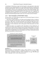
CHAPTER 1
Built-in
Self-Test
B
efore we proceed to present the major elements of the ABIST methodol
ogy, we would like to provide the reader with a brief overview of existing
built-in self-test (BIST) principles and the resulting practical solutions. Sub
sequently, this part of the book can be used as a reference when studying the
remaining chapters, especially 2 and 3. Since BIST can be regarded as a natural
outgrowth of design for testability (DFT), we begin this chapter by introducing
several issues underlying DFT mechanisms and putting BIST into perspective
by examining the reasons for its emergence. We will then look at a variety of
BIST schemes which have evolved over the years for generating test patterns
and analyzing the resultant circuit response. The chapter concludes with BIST
applications and, in particular, testing approaches for general and structured
logic which are used in custom and semicustom designs.
1.1
Introduction
Current trends in semiconductor technologies, as well as in design methodolo
gies, readily indicate that the ever-increasing degree of integration of devices on
a single substrate continuously demands more efforts in achieving zero-defect
designs. Clearly, this ultimate quality goal cannot be met without including
testability as a design objective. Although the process of integration, strongly
supported by CAD tools, has already led to an improved quality of integrated
circuits, adding testability to a number of criteria considered during design, such
as performance, area, power, manufacturability, etc., may significantly enhance
the reliability of products and their overall quality.
Testability, although difficult to define and quantify because of the many
different factors affecting costs and quality of testing, reflects ability of the
2
1. Built-in Self-Test
circuit's tests to detect, and possibly locate, failures causing malfunctioning of
the circuit. As the number and kind of faults that may occur depends on the
type of device and a technology used to fabricate it, evaluation of test quality can
be a difficult and often computationally intensive process. Ideally, we would like
to measure a defect level representing the fraction of faulty chips within those
passed as good by the tests. It is, however, difficult to obtain an accurate defect
level, as it requires the knowledge of yield and statistical properties of defects.
Consequently, an indirect and easier-to-estimate test quality measure is used.
It is called fault coverage and is defined as the ratio of the number of faults
that can be detected to the total number of faults in the assumed fault domain.
As the complexity of electronic devices continues to increase, the complete fault
coverage, one of the primary quality requirements, becomes more and more
difficult to achieve by virtue of only traditional testing paradigms.
The growth in the cost of developing and applying tests is attributable to
almost the trivial observation that modern complex integrated circuits pose very
serious problems in testing and debugging. Testing at the board or complete
system level can be even more difficult. On the other hand, there is a contin
uing need for testing in these various architectural stages. At the chip-level,
testability problems include:
• a very high and still increasing logic-to-pin ratio, which points out a highly
unbalanced relationship between a limited number of input/output ports
and unprecedently complex semiconductor devices which are accessible
only through these terminals,
• a circuit complexity which continues to grow as new submicron technolo
gies offer higher densities and speeds,
• an increasingly long test-pattern generation and test application time; it
has been repeatedly reported that functional and random tests for general
class of circuits containing memory elements have very low fault coverage;
in the case of deterministic patterns, an extraordinary amount of process
ing time might be required to generate a test vector, and then it may take
a large number of clock cycles to excite a fault and propagate it to primary
outputs,
• a prohibitively large volume of test data that must be kept by testing
equipment,
• an inability to perform at-speed testing through external testing equip
ment,
• incomplete knowledge of the gate level structure as designers are separated
from the level of implementation by automated synthesis tools,
3
1.1. Introduction
• lack of methods and metrics to measure the completeness of employed
testing schemes,
• difficulties in finding skilled resources.
At the printed circuit board level, external testers would require a sophisti
cated bed-of-nails fixture in order to access the pins of the chips on the board, if
these circuits were designed without addressing testability issues. This expen
sive technique becomes virtually impractical when a surface-mount technology
is used with components mounted densely on both sides of the board. Also, as
the board has to be removed from the system, system-level diagnosis becomes
impossible.
It is certainly imperative to keep all costs related to testing, and originating
from the above mentioned problems, in reasonable bounds. It appears that this
can be accomplished at the expense of a modest amount of area and possible
minimal performance degradation such that a uniform and structured solution
can be used in debugging, manufacturing, and system testing. This desired
approach, or rather a collection of techniques which make the final design eco
nomically testable, is known as a process of design for testability (DFT). DFT
is expected to produce circuits with adequate controllability and observability,
satisfying several design rules which reduce test development costs, increase
fault coverage, and finally, reduce defect levels.
Although several testability problems can be alleviated by using certain DFT
techniques, the actual testing still requires the application of test stimuli and
the comparison of test responses with the correct reference. These operations
are traditionally carried out by means of external testing equipment such that
the tester applies test vectors one by one and then compares the responses
with the fault-free responses, also one by one. For large circuits this approach
becomes infeasible. As we have indicated above, the patterns can be difficult to
generate and the number of tests can be so large that it would be difficult to
store and handle them efficiently by the tester hardware. The time to apply the
vectors may become unacceptable. In addition, the testers are very expensive,
and testing cannot be performed once the device is in the system.
An attractive alternative to the classical testing scenario, where test patterns
are applied from an external tester, is built-in self-test (BIST). In BIST, an
additional "on-chip" circuitry is included to generate test vectors, evaluate test
responses, and control the test. Random, or in fact pseudo-random, patterns
can be generated by simple circuits, and test responses can be compacted into
a short statistic by calculating a signature. This signature, obtained from the
CUT, can be subsequently compared with a fault-free signature.
BIST has revolutionized the way the integrated circuits can be tested. It
reduces the cost of manufacturing testing by shortening the test application
/
4
1. Built-in Self-Test
time, minimizing the amount of test data stored, and lowering the cost of test
ing equipment. Its implementation can result in a reduction of the product
development cycle and cost, as well as a reduction of the cost of system main
tenance. The latter benefits may have a dramatic impact on the economics of
testing. It follows from the fact that built-in test circuitry can test chips, boards,
and the entire system virtually without very expensive external automatic test
equipment. The ability to run tests at different levels of the system's hierarchy
significantly simplifies diagnostic testing, which in turn improves troubleshoot
ing procedures and sanity checks during assembly, integration, and field service.
Since the BIST hardware is an integral part of the chip, BIST, in principle,
could allow for at-speed testing, thus covering faults affecting circuit timing
characteristics.
The basic BIST objectives are often expressed with respect to test-pattern
generation and test-response compaction. It is expected that appending BIST
circuitry to the circuit under test will result in high fault coverage, short test
application time, small volume of test data, and compatibility with the assumed
DFT methodology. High fault coverage in BIST can be achieved only if all faults
of interest are detected and their effects are retained in the final signature after
compaction. Numerous test generation and test-response compaction techniques
have been proposed in the open literature and are used in industrial practice
as implementation platforms to cope with these objectives for various types of
failures, errors, and a variety of test scenarios. In the following subsections we
will outline several schemes used in different BIST environments. They have
gained a wide acceptance by BIST practitioners, and their superiority over nonBIST approaches ensures a successful applicability of BIST in current and future
technologies.
Clearly, the use of BIST is also associated with certain costs. Additional sili
con area is required for the test hardware to perform test-pattern generation and
test-response compaction. Some performance degradation may be introduced
due to the presence of multiplexers needed to apply the test patterns in the test
mode. Some testing equipment may still be needed to test the BIST hardware
and to carry out the parametric testing. BIST also requires more rigid design.
In particular, unknown states are not allowed since they can produce unknown
signatures. We will also return to these problems in the next subsections.
1.2
1.2.1
Design for Testability
Controllability and Observability
There are two major concepts which are commonly used in assessing and en
hancing the testability of a circuit under test: controllability and observability.
Controllability is a measure of how difficult it is to set a line to a value necessary
1.2. Design for Testability
5
to excite a fault. Observability is a measure of how difficult it is to propagate
a faulty signal from a line to a primary output. Notice that controllability, in
addition to its impact on a fault activation, also indirectly affects the ease with
which the required signals can be set to propagate fault effects. The essence
of design for testability is to apply minor changes to the original circuit de
sign such that the resultant controllability and observability will be improved.
The frequently used set of characteristics for controllability and observability of
each node in a circuit includes three values representing the relative degree of
difficulty of:
• achieving 1 at the node (1-controllability),
• achieving 0 at the node (0-controllability),
• driving the fault effects from the node to a primary output.
The above measures have to be used with respect to whether tests employed
are pseudo-random or deterministic. In the latter case, all measures can be
employed to guide an automatic test-pattern generation technique. In a BIST
environment, however, a common test scenario is to use the pseudo-random
patterns. Under such circumstances, the definitions of controllability and ob
servability can be restated in the following way [16]:
• 1-controllability (0-controllability) of a node is the probability that a ran
domly applied input vector will set the node to a value 1 (0),
• observability of a line is the probability that a randomly applied input
vector will sensitize one or more paths from that line to a primary output.
It can be easily observed that a circuit node will have a low controllability
and/or observability if a unique test vector or a long test sequence is required
to establish the state of this node and then to propagate this state to the outputs
of the circuit.
1.1 A circuit shown in Fig. 1.1, although easily initializable, is nev
ertheless extremely difficult to control. It consists of a microprogram memory
driven by a next address counter. The counter can be reset. Its next state, how
ever, can be either worked out by the counter itself (an increment function after
applying a clock pulse) or provided by the memory as a "branch" address if a
respective flag is set. In either case, it may take an enormous amount of time to
force several bits of the counter to certain values, especially if the memory con
tains a lengthy program whose execution depends on data. In other words, there
is no simple way to run all parts of the program in a systematic manner in order
EXAMPLE
1. Built-in Self-Test
6
Figure 1.1: Circuit difficult to control.
to exercise the entire address space. Furthermore, even totally sequential exe
cution of the program still requires 2 n - 1 clock pulses to set the most significant
bit of the counter to the value of 1, where n is the size of the counter.
The observations made so far indicate that the key to structural design
for testability is to have the ability to control and observe the state variables
directly. This can be accomplished by a number of DFT approaches described
in the following sections.
1.2.2
Ad Hoc Techniques
Several design techniques have been used over the years to avoid potential prob
lems with testing. They are termed "ad hoc" approaches, as they are mostly
aimed at designers and do not provide any systematic (algorithmic) method
ology which improves testability across the entire circuit. They do provide,
however, certain rules that must always be followed in order to increase con
trollability and observability. These rules are, in different ways, implemented
in more rigorous DFT designs, too. In the remainder of this section, we discuss
some of these approaches that have traditionally been applied to simplify testing
[2], [16].
Test points. Test points can be added to a circuit to make it easier to
either sensitize faults (control points) or to observe them (observation points).
Fig. 1.2 shows so-called 0- and 1-injection circuits where two extra gates are
used to achieve 0- and 1-controllability of a line connecting subcircuits C\ and
C 2 . For example, in the 1-injection circuitry, when TEST — 0, the circuit
1.2. Design for Testability
7
Figure 1.2: Control points to force 0 and 1.
operates in its normal mode. Setting TEST = 1 allows us to inject a 1 on line
S, and subsequently on line b of subcircuit C2,. Line S can be controlled by
an extra primary input, or it can be driven by a flip-flop being a part of the
internal scan path (see section 1.2.3). In general, optimal test point insertion in
circuits with reconvergent fanout is an NP-complete problem [104], and therefore
numerous empirical guidelines and approximate techniques have been proposed
to identify locations in a circuit to introduce control and observation points [25],
[39], [86], [147], [152]. In fact, almost every DFT technique listed below uses test
point insertion inherently to implement its underlying philosophy of improving
testability. Techniques for automatic test point insertion are also discussed in
section 1.2.5.
Internally generated clocks, monostable multivibrators, and oscillators. In
order to eliminate the need to synchronize the tester and pulses internal to a
circuit, these devices should be disabled during test. Furthermore, testing can
be performed at the speed of the tester rather than at the speed of the circuit.
Asynchronous logic. It should be avoided by designers as circuits with asyn
chronous feedback loops are susceptible to hazards. Although it is possible to
omit a hazard by using an appropriate ATPG tool which takes into account tim
ing delays in the circuit, it can be very expensive. In many cases (for example,
pseudo-random testing) avoiding hazards is practically impossible.
Initialization. A sequential circuit must be brought into a known state before
its actual testing. This can be achieved by using a customized initialization
sequence. However, as such a sequence is usually devised by a designer, it is
unlikely that it will exhibit enough simplicity to be recreated by ATPG software
or to be used in a BIST environment. Thus, it is recommended to employ reset
or set inputs to flip-flops or another simple presetting circuitry.
Logical redundancy. Unless added intentionally to eliminate hazards and
races or to increase reliability, a logical redundancy is a highly undesirable
phenomenon which should be completely avoided. The presence of redundancy
causes ATPG tools to waste a lot of time while trying to generate nonexistent
1. Built-in Self-Test
8
tests for redundant faults. Moreover, redundant faults may invalidate tests
for nonredundant faults. Unfortunately, the redundancy is often introduced
inadvertently and is therefore extremely difficult to identify and remove.
Global feedback paths. Since from the ATPG point of view the feedback paths
may introduce very long gate paths, they should be eliminated. The simplest
way of achieving this objective is to use control points or another logic to break
the paths during testing.
Long counters and shift registers. As shown in the last example, the long
counter may require an unacceptable number of clock cycles to change the most
significant bits. A common remedy is to add the control points, such that
the counter (or a shift register) is partitioned into smaller units, which can be
clocked a much lesser number of times to set significant bits.
Memory arrays and other embedded structures. Memory arrays should be
isolated from the remaining parts of a circuit for at least two reasons. First,
it is very difficult to generate tests for circuits with memory blocks. Second,
when separated, a stand-alone memory circuitry can be conveniently tested by
means of a variety of test schemes developed particularly for these structures.
The same methodology applies to other embedded logic blocks, such as PL As,
cores, etc.
Large combinational circuits. Because of the time complexity of test genera
tion and fault simulation, it is justified to partition large circuits in order to test
them separately. Partitioning simplifies the task of fault excitation, fault prop
agation, and line value justification in ATPG, in addition to increasing random
pattern testability. The independent testing of the resultant partitions is carried
out through the number of test points added to lines crossing partition bound
aries. Fig. 1.3b illustrates such a partitioning [2] of a circuit shown in Fig. 1.3a.
Control inputs T1 and T2 are used to test separately either C1 (T1T2 = 01), or
C2 (T1T2 = 10), or to put the circuit into a normal mode (T1T2 = 00).
1.2.3
Scan Designs
In order to test complex circuits in a time and cost-effective manner, a number
of structured design techniques have been proposed. They rest on the general
concept of making all or some state variables (memory elements) directly con
trollable and observable. If this can be arranged, a circuit can be treated, as
far as testing of combinational faults is concerned, as a combinational network.
Perhaps the most used and best-known is a family of techniques termed scan
designs. They assume that during testing all registers (flip-flops and latches) in
a sequential circuit are connected into one or more shift registers or scan paths.
The circuit has two modes of operation:
• normal mode - the memory elements perform their regular functions (as
in an unmodified circuit),
1.2. Design for Testability
9
a)
Figure 1.3: Partitioning of a circuit.
• test (scan) mode - all the memory elements connected into a shift register
are used to shift in (or scan in) and out test data.
During testing the sequence of operations for scan-based designs is as follows:
1. Select the test mode (memory elements form a shift register).
2. Shift in test-pattern values into the flip-flops.
3. Set the corresponding values on the primary inputs.
4. Select the normal mode.
5. After the logic values have had time to settle, check the primary output
values and subsequently capture a test response into the flip-flops.
6. Select the test mode. Shift out the flip-flop contents and compare them
with good response values. The next input vector can be shifted in at the
same time.
7. Repeat steps 2 through 6 for successive test vectors.
The flip-flops are tested by means of a "flush test" consisting of either a string
of 1Is followed by a string of 0s, or a serial pattern 00110011... used to check if
each flip-flop can hold 0 and 1 and make transitions.
10
1. Built-in Self-Test
The scan-based designs must comply with a set of design rules and con
straints. Usually, they are related to design methods for scan cells and con
sequently determine a type of DFT style which is adopted for a given circuit.
Nevertheless, several common advantages of scan-based DFT schemes can be
easily pronounced. They include:
• simplified test-pattern generation and test-pattern evaluation - testing the
network is essentially the same as that of testing a combinational circuit,
• simplified timing analysis - proper operation of the network is independent
of clock characteristics and only requires the clock pulse to be active for
a sufficient period,
• simplified design validation - automated checks for design rule violation
can be performed with relative ease,
• very few additional external pins (usually three or four) are required to
access the system flip-flops,
• easier design debugging - the scan paths provide the direct access to many
internal circuit nodes.
Clearly, there are some inevitable limitations of the scan designs. They
introduce additional hardware (area overhead), performance degradation (due
to the presence of multiplexers in shift register latch designs), and increased test
application time (because of scan-in and scan-out operations). Furthermore, it
might be difficult to test the circuit at its operational speeds and therefore the
coverage of some faults, especially delays, can be low. In addition, all timing
is usually controlled by an external clock, and there is a need to incorporate a
design rule checking into CAD software in order to automate the design process.
Fig. 1.4 illustrates a basic scan-path design. As can be seen, the circuit
features three extra pins (test mode, scan-in, scan-out) as well as area and
performance overhead due to the multiplexers. When the test mode signal is
low, the circuit operates in its normal, that is, parallel-latch mode, except for
increased delays. In the test mode, test patterns are shifted in through the
scan-in terminal, and test responses are subsequently shifted out through the
scan-out pin.
There are several forms of scan design, among them the scan path [63], the
scan/set [157], the random-access scan [11], and the level-sensitive scan design
(LSSD) [60] used in many IBM products. For the sake of illustration, we will
briefly discuss the LSSD technique. The memory elements used by LSSD are
implemented as latches in which the stored data cannot be changed by any
input when the clocks are off. Moreover, each latch is augmented to form a
shift-register latch (see Fig. 1.5 on page 12) by adding an extra latch (L2)
1.2. Design for Testability
11
Figure 1.4: Basic scan-design architecture.
with a separate clock input. Interconnection of the latches into a shift register
structure is done as shown in Fig. 1.5, which demonstrates the general structure
for a so-called LSSD double-latch design. In this approach, both latches, LI and
L2, are used as system latches, and the circuit output is taken from outputs of
L2. Note that, in the normal mode, clocks C2 and C3 are used, while in the test
mode, nonoverlapping clocks C1 and C2 are used to prevent races. The scan
path is denoted by the dashed line. Another LSSD approach, known as a singlelatch design, is also used if it is desired to separate combinational circuits only
by a single latch. In this solution, latches L2 are not employed to perform the
system functions of the circuit. Several variations of the original LSSD design
have been also proposed [2], mostly to reduce logic complexity.
To reduce the costs of using scan designs, especially area overhead and per
formance degradation, several partial scan techniques have been proposed in
which only a subset of the circuit memory elements are included in the scan
path. Among these methods, there are three common strategies used to se
lect the flip-flops to scan such that the cost of test-pattern generation is re
duced while the testability overheads are minimized. Chronologically, the first
approach was to employ testability measures in the flip-flop selection process
[171]. It does not guarantee the optimal solution as testability measures are
usually not accurate and do not characterize the global effects. The second
group of methods is based on breaking cyclic paths in the CUT [38] in order
to reduce the number of the feedback loops and their sequential depth. The
rationale behind these techniques is to reduce the high cost of sequential ATPG
originating from the presence of these loops. A special variant of this method
cuts all the feedback loops, so that during test the resulting circuit works as
1. Built-in Self-Test
12
Figure 1.5: LSSD double-latch design.
a pipeline where faults can be processed by a combinational ATPG [71]. The
third concept utilizes test-pattern generation techniques [110]. The partial scan
can be conveniently integrated with various BIST schemes [109], similarly to
solutions used in the full scan environment. The reader may find further details
in section 1.5.
1.2.4
Boundary-Scan Architecture
As we have already mentioned, one of the major advantages of BIST is its ability
to operate at different levels of a circuit's architectural hierarchy. However, in
order to invoke the BIST procedures and facilitate their correct execution at the
board, module or system level, certain design rules must be applied. In 1990, a
new testing standard was adopted by the Institute of Electrical and Electronics
Engineers, Inc., and it is now defined as the IEEE Standard 1149.1, IEEE
Standard Test Access Port and Boundary-Scan Architecture. Its overview can
be found in [111]. The basic architecture of the boundary scan is incorporated at
the integrated circuit level and essentially consists of a protocol by which various
test functions can be carried out. In particular, the standard defines four (or
optionally, five) new pins forming the test access port (TAP - see Fig. 1.6):
two of them (test clock TCK and test mode select TMS) are used to control the
protocol, while the remaining two pins (test data in TDI and test data out TDO)