Modern Aspects of Spin Physics-Walter Pötz Jaroslav Fabian, Ulrich Hohenester
Bạn đang xem bản rút gọn của tài liệu. Xem và tải ngay bản đầy đủ của tài liệu tại đây (2.74 MB, 139 trang )
Lecture Notes in Physics
Editorial Board
R. Beig, Wien, Austria
W. Beiglböck, Heidelberg, Germany
W. Domcke, Garching, Germany
B.-G. Englert, Singapore
U. Frisch, Nice, France
P. Hänggi, Augsburg, Germany
G. Hasinger, Garching, Germany
K. Hepp, Zürich, Switzerland
W. Hillebrandt, Garching, Germany
D. Imboden, Zürich, Switzerland
R. L. Jaffe, Cambridge, MA, USA
R. Lipowsky, Golm, Germany
H. v. Löhneysen, Karlsruhe, Germany
I. Ojima, Kyoto, Japan
D. Sornette, Nice, France, and Zürich, Switzerland
S. Theisen, Golm, Germany
W. Weise, Garching, Germany
J. Wess, München, Germany
J. Zittartz, Köln, Germany
The Lecture Notes in Physics
The series Lecture Notes in Physics (LNP), founded in 1969, reports new developments
in physics research and teaching – quickly and informally, but with a high quality and
the explicit aim to summarize and communicate current knowledge in an accessible way.
Books published in this series are conceived as bridging material between advanced graduate textbooks and the forefront of research to serve the following purposes:
• to be a compact and modern up-to-date source of reference on a well-defined topic;
• to serve as an accessible introduction to the field to postgraduate students and nonspecialist researchers from related areas;
• to be a source of advanced teaching material for specialized seminars, courses and
schools.
Both monographs and multi-author volumes will be considered for publication. Edited
volumes should, however, consist of a very limited number of contributions only. Proceedings will not be considered for LNP.
Volumes published in LNP are disseminated both in print and in electronic formats,
the electronic archive is available at springerlink.com. The series content is indexed,
abstracted and referenced by many abstracting and information services, bibliographic
networks, subscription agencies, library networks, and consortia.
Proposals should be sent to a member of the Editorial Board, or directly to the managing
editor at Springer:
Dr. Christian Caron
Springer Heidelberg
Physics Editorial Department I
Tiergartenstrasse 17
69121 Heidelberg/Germany
Walter Pötz Jaroslav Fabian
Ulrich Hohenester (Eds.)
Modern Aspects
of Spin Physics
ABC
Editors
Walter Pötz
Ulrich Hohenester
Institut für Theoretische Physik
Universität Graz
Universitätsplatz 5
8010 Graz, Austria
E-mail:
Jaroslav Fabian
Institut für Theoretische Physik
Universität Regensburg
Universitätsstr. 31
93040 Regensburg, Germany
E-mail:
Walter Pötz et al., Modern Aspects of Spin Physics, Lect. Notes Phys. 712 (Springer,
Berlin Heidelberg 2007), DOI 10.1007/b11824190
Library of Congress Control Number: 2006931572
ISSN 0075-8450
ISBN-10 3-540-38590-8 Springer Berlin Heidelberg New York
ISBN-13 978-3-540-38590-5 Springer Berlin Heidelberg New York
This work is subject to copyright. All rights are reserved, whether the whole or part of the material is
concerned, specifically the rights of translation, reprinting, reuse of illustrations, recitation, broadcasting,
reproduction on microfilm or in any other way, and storage in data banks. Duplication of this publication
or parts thereof is permitted only under the provisions of the German Copyright Law of September 9,
1965, in its current version, and permission for use must always be obtained from Springer. Violations are
liable for prosecution under the German Copyright Law.
Springer is a part of Springer Science+Business Media
springer.com
c Springer-Verlag Berlin Heidelberg 2007
The use of general descriptive names, registered names, trademarks, etc. in this publication does not imply,
even in the absence of a specific statement, that such names are exempt from the relevant protective laws
and regulations and therefore free for general use.
Typesetting: by the authors and techbooks using a Springer LATEX macro package
Cover design: WMXDesign GmbH, Heidelberg
Printed on acid-free paper
SPIN: 11824190
54/techbooks
543210
Preface
This volume contains a collection of lecture notes provided by the key speakers of the Schladming Winter School in Theoretical Physics, “43. Internationale Universit¨
atswochen f¨
ur Theoretische Physik”, held in Schladming,
Austria. This school took place from February 26 till March 4, 2005, and was
titled Spin Physics, Spintronics, and Spin-Offs.
Until 2003 the Schladming Winter School, which is organized by the Division for Theoretical Physics of the University of Graz, Austria, has been
devoted primarily to topics in subatomic physics. A few years ago, however,
it was decided to broaden the scope of this school and, in particular, to incorporate hot topics in condensed matter physics. This was done in an effort
to better represent the scientific activities of the theory group of the Physics
Department at the University of Graz, resulting in the 42nd Winter School on
“Quantum Coherence in Matter: From Quarks to Solids,” held in 2004, and
the 43rd Winter School on “Spin Physics, Spintronics, and Spin-Offs” in 2005.
A compilation of lecture notes from the 2004 event have been released in the
Springer series Lecture Notes in Physics LNP689 titled Quantum Coherence:
From Quarks to Solids.
Spin is a fundamental property of elementary particles with important
consequences on the macroscopic world. Beginning with the famous Stern–
Gerlach experiment, research has been conducted to provide a sound microscopic understanding of this intriguing physical property. Indeed, the spin
degree of freedom has physical implications on practically all areas of physics
and beyond: from elementary particle physics, atomic-molecular physics, condensed matter physics, optics, to chemistry and biology.
Recently, the spin degree of freedom has been “rediscovered” in the context of quantum information storage and processing, colloquially summarized
as “quantum computation.” In addition, a relatively young field of solid-state
device physics termed “spintronics,” with the attempt to utilize the spinrather than the charge-degree of freedom, has emerged. Each of these two
topics is well worthy of its own school; however, in an attempt to provide
an even broader perspective and to also attract students from elementary
particle physics this winter school has included not only lectures and talks
from both fields, but topics from elementary particle physics as well. As in
past years, the Schladming Winter School and this compilation of lecture
VI
Preface
notes is intended for advanced undergraduate and graduate students up to
senior scientists who want to learn about or even get into this exciting field of
physics. Research in this area is interdisciplinary and has both fundamental
and applied aspects.
Listed below, in alphabetical order, are the speakers and titles of their
lectures:
Enrico Arrigoni, Technical University of Graz, “Spin Pairing and HighTemperature Superconductors”
Tomasz Dietl, Polish Academy of Sciences, Warsaw, “Semiconductor Spintronics”
Stefano Forte, University of Milano, “Spin in Quantum Field Theories”
Elliot Leader, Imperial College, London, “Nucleon Spin”
Yuli V. Nazarov, Delft University, “Spin Currents and Spin Counting”
ˇ c, NRL, Washington DC, “Spin-Polarized Transport in SemiconIgor Zuti´
ductor Junctions: From Superconductors to Magnetic Bipolar Transistors”
Next to these lectures, there were a number of invited and contributed
talks. For details, we refer to our Schladming Winter School web page
This volume contains the
lecture notes presented by T. Dietl, E. Arrigoni, S. Forte, and E. Leader.
What has been said before about the flavor of the lectures also applies to the
lecture notes presented in this volume.
In “Semiconductor Spintronics,” Tomasz Dietl gives an overview of the
modern field of spintronics, containing a brief history, motivation behind the
field, past achievements, and future challenges. It should be mentioned that
Prof. Dietl’s Award of the Agilent Technologies Europhysics Prize 2005 (with
David D. Awschalom and Hideo Ohno) was announced during the Winter
School.
In “Lectures on Spin Pairing Mechanism in High-Temperature Superconductors,” Enrico Arrigoni first reviews the essentials of conventional phononbased superconductivity and then discusses alternative pairing mechanisms
based on the Hubbard model, which may play a role in high-temperature
superconducting materials with an antiferromagnetic phase.
In “Spin in Quantum Field Theories,” Stefano Forte gives a pedagogical introduction to spin in quantum field theory, largely avoiding the usual
framework of relativistic quantum field theory. This paper is intended as a
bridge between elementary particle (relativistic quantum field theory) physics
and condensed matter physics (nonrelativistic quantum field theory).
In “Nucleon Spin,” Elliot Leader discusses proton (nucleon) spin and pitfalls encountered in the interpretation of its origin from the nucleon’s constituents.
We are grateful to the lecturers for presenting their lectures in a very
pedagogical way at the school and for taking the time for preparing the
Preface
VII
manuscripts for publication in this book. We feel that this volume represents
a good overview of current research on spin-related physics.
We acknowledge financial support from the main sponsors of the school:
the Austrian Federal Ministry of Education, Science, and Culture, as well as
the Government of Styria. We have received financial, material, and technical support from the University of Graz, the town of Schladming, RICOH
Austria, and Hornig Graz. We also thank our colleagues, staff, and students
at the Physics Department for their valuable technical assistance, as well as
all participants and speakers for making the 43rd Schladming Winter School
a great success.
Graz,
July 2006
Walter P¨
otz
Jaroslav Fabian
Ulrich Hohenester
Contents
Semiconductor Spintronics
T. Dietl . . . . . . . . . . . . . . . . . . . . . . . . . . . . . . . . . . . . . . . . . . . . . . . . . . . . . . . .
1
2
Why Spintronics? . . . . . . . . . . . . . . . . . . . . . . . . . . . . . . . . . . . . . . . . . . .
Non-magnetic Semiconductors . . . . . . . . . . . . . . . . . . . . . . . . . . . . . . . .
2.1 Overview . . . . . . . . . . . . . . . . . . . . . . . . . . . . . . . . . . . . . . . . . . . . . .
2.2 Spin Relaxation and Dephasing . . . . . . . . . . . . . . . . . . . . . . . . . . .
2.3 An Example of Spin Filter . . . . . . . . . . . . . . . . . . . . . . . . . . . . . . .
3 Hybrid Structures . . . . . . . . . . . . . . . . . . . . . . . . . . . . . . . . . . . . . . . . . . .
3.1 Overview . . . . . . . . . . . . . . . . . . . . . . . . . . . . . . . . . . . . . . . . . . . . . .
3.2 Spin Injection . . . . . . . . . . . . . . . . . . . . . . . . . . . . . . . . . . . . . . . . . .
3.3 Search for Solid-state Stern-Gerlach Effect . . . . . . . . . . . . . . . . .
4 Diluted Magnetic Semiconductors . . . . . . . . . . . . . . . . . . . . . . . . . . . . .
4.1 Overview . . . . . . . . . . . . . . . . . . . . . . . . . . . . . . . . . . . . . . . . . . . . . .
4.2 Magnetic Impurities in Semiconductors . . . . . . . . . . . . . . . . . . . .
4.3 Exchange Interaction Between Band and Localized Spins . . . .
4.4 Electronic Properties . . . . . . . . . . . . . . . . . . . . . . . . . . . . . . . . . . . .
4.5 Magnetic Polarons . . . . . . . . . . . . . . . . . . . . . . . . . . . . . . . . . . . . . .
4.6 Exchange Interactions between Localized Spins . . . . . . . . . . . . .
4.7 Magnetic Collective Phenomena . . . . . . . . . . . . . . . . . . . . . . . . . .
5 Properties of Ferromagnetic Semiconductors . . . . . . . . . . . . . . . . . . . .
5.1 Overview . . . . . . . . . . . . . . . . . . . . . . . . . . . . . . . . . . . . . . . . . . . . . .
5.2 p-d Zener Model . . . . . . . . . . . . . . . . . . . . . . . . . . . . . . . . . . . . . . . .
5.3 Curie Temperature – Chemical Trends . . . . . . . . . . . . . . . . . . . . .
5.4 Micromagnetic Properties . . . . . . . . . . . . . . . . . . . . . . . . . . . . . . . .
5.5 Optical Properties . . . . . . . . . . . . . . . . . . . . . . . . . . . . . . . . . . . . . .
5.6 Charge Transport Phenomena . . . . . . . . . . . . . . . . . . . . . . . . . . . .
5.7 Spin Transport Phenomena . . . . . . . . . . . . . . . . . . . . . . . . . . . . . .
5.8 Methods of Magnetization Manipulation . . . . . . . . . . . . . . . . . . .
6 Summary and Outlook . . . . . . . . . . . . . . . . . . . . . . . . . . . . . . . . . . . . . . .
References . . . . . . . . . . . . . . . . . . . . . . . . . . . . . . . . . . . . . . . . . . . . . . . . . . . . .
1
1
4
4
5
6
7
7
8
9
11
11
12
14
15
17
17
18
19
19
20
22
23
26
28
36
37
37
40
X
Contents
Lectures on the Spin Pairing Mechanism in High-Temperature
Superconductors
E. Arrigoni . . . . . . . . . . . . . . . . . . . . . . . . . . . . . . . . . . . . . . . . . . . . . . . . . . . . 47
1
2
3
4
5
6
Introduction . . . . . . . . . . . . . . . . . . . . . . . . . . . . . . . . . . . . . . . . . . . . . . . .
Superconductivity . . . . . . . . . . . . . . . . . . . . . . . . . . . . . . . . . . . . . . . . . . .
Phonon-Mediated Effective Attraction between Electrons . . . . . . . .
BCS Theory . . . . . . . . . . . . . . . . . . . . . . . . . . . . . . . . . . . . . . . . . . . . . . .
High-Temperature Superconductors . . . . . . . . . . . . . . . . . . . . . . . . . . . .
Pairing Mediated by Spin Fluctuations:
Linear Response to Magnetic Excitations . . . . . . . . . . . . . . . . . . . . . . .
References . . . . . . . . . . . . . . . . . . . . . . . . . . . . . . . . . . . . . . . . . . . . . . . . . . . . .
47
48
50
53
55
59
65
Spin in Quantum Field Theory
S. Forte . . . . . . . . . . . . . . . . . . . . . . . . . . . . . . . . . . . . . . . . . . . . . . . . . . . . . . . 67
1
2
From Quantum Mechanics to Field Theory . . . . . . . . . . . . . . . . . . . . .
Spin and Statistics . . . . . . . . . . . . . . . . . . . . . . . . . . . . . . . . . . . . . . . . . .
2.1 The Galilei Group and the Lorentz Group . . . . . . . . . . . . . . . . .
2.2 Statistics and Topology . . . . . . . . . . . . . . . . . . . . . . . . . . . . . . . . . .
2.3 Bosons, Fermions and Anyons . . . . . . . . . . . . . . . . . . . . . . . . . . . .
3 A Path Integral for Spin . . . . . . . . . . . . . . . . . . . . . . . . . . . . . . . . . . . . .
3.1 The Spin Action . . . . . . . . . . . . . . . . . . . . . . . . . . . . . . . . . . . . . . . .
3.2 Classical Dynamics . . . . . . . . . . . . . . . . . . . . . . . . . . . . . . . . . . . . .
3.3 Geometric Quantization . . . . . . . . . . . . . . . . . . . . . . . . . . . . . . . . .
4 Relativistic Spinning Particles . . . . . . . . . . . . . . . . . . . . . . . . . . . . . . . .
4.1 Path Integral for Spinless Particles . . . . . . . . . . . . . . . . . . . . . . . .
4.2 The Classical Spinning Particle . . . . . . . . . . . . . . . . . . . . . . . . . . .
4.3 Quantum Spinning Particles and Fermions . . . . . . . . . . . . . . . . .
5 Conclusion . . . . . . . . . . . . . . . . . . . . . . . . . . . . . . . . . . . . . . . . . . . . . . . . .
References . . . . . . . . . . . . . . . . . . . . . . . . . . . . . . . . . . . . . . . . . . . . . . . . . . . . .
67
68
68
70
74
79
79
81
82
86
86
88
90
93
94
Nucleon Spin
E. Leader . . . . . . . . . . . . . . . . . . . . . . . . . . . . . . . . . . . . . . . . . . . . . . . . . . . . . . 95
1
2
3
4
5
6
7
8
Introduction . . . . . . . . . . . . . . . . . . . . . . . . . . . . . . . . . . . . . . . . . . . . . . . .
Polarized Lepton-Nucleon Deep Inelastic Scattering . . . . . . . . . . . . . .
The Spin Crisis in the Parton Model . . . . . . . . . . . . . . . . . . . . . . . . . . .
Resolution of the Spin Crisis: The Axial Anomaly . . . . . . . . . . . . . . .
Matrix Elements of Angular Momentum Operators: The Problem .
Relativistic Spin States . . . . . . . . . . . . . . . . . . . . . . . . . . . . . . . . . . . . . .
Matrix Elements of Angular Momentum Operators: The Results . .
7.1 Canonical Spin State Matrix Elements . . . . . . . . . . . . . . . . . . . . .
7.2 Helicity State Matrix Elements . . . . . . . . . . . . . . . . . . . . . . . . . . .
Angular Momentum Sum Rules . . . . . . . . . . . . . . . . . . . . . . . . . . . . . . .
8.1 General Structure of Sum Rules:
Parton Transverse Momentum . . . . . . . . . . . . . . . . . . . . . . . . . . . .
95
97
101
105
108
111
113
114
116
118
118
Contents
8.2 The Longitudinal Sum Rule . . . . . . . . . . . . . . . . . . . . . . . . . . . . . .
8.3 The Transverse Case: The New Sum Rulexs . . . . . . . . . . . . . . . .
8.4 Comparison with Results in the Literature . . . . . . . . . . . . . . . . .
9 Interpretation of the Sum Rules . . . . . . . . . . . . . . . . . . . . . . . . . . . . . . .
References . . . . . . . . . . . . . . . . . . . . . . . . . . . . . . . . . . . . . . . . . . . . . . . . . . . . .
XI
122
123
125
126
127
List of Contributors
Enrico Arrigoni
Institute for Theoretical Physics
and Computational Physics
Graz University of Technology
Petersgasse 16
A-8010 Graz
Austria
Tomasz Dietl
Institute of Physics
Polish Academy of Sciences
and
ERATO Semiconductor Spintronics
Project
Japan Science and Technology
Agency
al. Lotnikow 32/46
PL-02668 Warszawa
Poland
and
Institute of Theoretical Physics
Warsaw University
Poland
Stefano Forte
Dipartimento di Fisica
Universita di Milano
and
INFN Sezione di Milano
via Celoria 16
I-10129 Milano
Italy
Elliot Leader
Prince Consort Road
London SW7 2BW
England
Semiconductor Spintronics
T. Dietl
Institute of Physics, Polish Academy of Sciences and ERATO Semiconductor
Spintronics Project, Japan Science and Technology Agency, al. Lotnik´
ow 32/46,
02668 Warszawa, Poland and Institute of Theoretical Physics, Warsaw University,
Poland
Abstract. These informal lecture notes describe the recent progress in semiconductor spintronics in a historic perspective as well as in comparison to achievements of spintronics of ferromagnetic metals. After outlining motivations behind
spintronic research, selected results of investigations on three groups of materials are presented. These include non-magnetic semiconductors, hybrid structures
involving semiconductors and ferromagnetic metals, and diluted magnetic semiconductors either in paramagnetic or ferromagnetic phase. Particular attention is
paid to the hole-controlled ferromagnetic systems whose thermodynamic, micromagnetic, transport, and optical properties are described in detail together with
relevant theoretical models.
1 Why Spintronics?
The well-known questions fuelling a broad interest in nanoscience are: will
it still be possible to achieve further progress in information and communication technologies simply by continuing to miniaturize the transistors in
microprocessors and the memory cells in magnetic and optical discs? How
to reduce power consumption of components in order to save energy and to
increase battery operation time? How to integrate nowadays devices with
biological molecules and functionalities?
Since 70s, the miniaturization by obeying Moore’s law has persistently
lead to an exponential increase in the quantity of information that can be
processed, stored, and transmitted per unit area of microprocessor, memory,
and fiberglass, respectively. A modern integrated circuit contains now one
billion transistors, each smaller than 100 nm in size, i.e., a five hundred times
smaller than the diameter of a human hair. The crossing of this symbolic
100 nm threshold at the outset of the 21st century ushered in the era of
nanotechnology. As the size of transistors decreases, their speed increases,
and their price falls. Today it is much less expensive to manufacture one
transistor than to print a single letter. Despite the series of successes that
industrial laboratories have scored over the past 40 years in surmounting one
technical and physical barrier after another, there is a prevalent sense that
in the near future a qualitative change is now in store for us in terms of the
methods of data processing, storing, encoding, and transmission. For this reason, governments in many countries are financing ambitious interdisciplinary
T. Dietl: Semiconductor Spintronics, Lect. Notes Phys. 712, 1–46 (2007)
c Springer-Verlag Berlin Heidelberg 2007
DOI 10.1007/3-540-38592-4 1
2
T. Dietl
programs aimed at insuring active participation in the future development of
nanotechnology.
Among the many proposals for where to take such research, the field of
spintronics, i.e., electronics aimed at understanding electron spin phenomena
and at proposing, designing, and developing devices to harness these phenomena, is playing a major role. The hopes placed in spintronics are founded
on the well-known fact that since magnetic monopoles do not exist, random
magnetic fields are significantly weaker than random electric fields. For these
reasons, magnetic memories are non-volatile, while memories based on an
accumulated electric charge (dynamic random access memory, or DRAM)
require frequent refreshing.
One of the ambitious goals in the spintronics field is to create magnetic
random access memory (MRAM), a type of device that would combine the
advantages of both magnetic memory and dynamic random access memory.
This requires novel methods of magnetizing memory cells and reading back
the direction of such magnetization, which would not involve any mechanical
systems. Another important step along this path would be the ability to control magnetization isothermally, by means of light or electric field. Modern
devices expend relatively large amounts of energy on controlling magnetization (i.e., storing data), as they employ Oersted magnetic fields generated by
electric currents.
The development of more “intelligent” magnetization control methods
would also make it possible to build spin transistors, devices composed of
two layers of ferromagnetic conductors separated by non-magnetic material. It stands to reason that if carriers injected into the non-magnetic layer
preserve their spin direction, then the electric conductivity depends on the
relative direction of the magnetization vectors in the ferromagnetic layers.
This could offer a means of producing an energy-conserving and fast switching device, as it would allow current to be controlled without changing the
carrier concentration. An obvious prerequisite for such a transistor to operate is the efficient injection of spin-polarized carriers made of ferromagnetic
material into the non-magnetic area. Also, there should be no processes that
could disrupt the spin polarization. Simultaneously, researchers are seeking
ways of generating, amplifying, and detecting spin currents: here, the underlying conviction is that the movement of electrons with opposite spins does
not entail any losses, yet can carry information. This would lay the foundations for the development of low-power devices, characterized by significantly
reduced heat dissipation. Another important issue is to develop methods for
injecting spin-polarized carriers into semiconductors. Apart from the possibility of designing the magnetization sensors and spin transistors, polarized
carrier injection could prove to be useful as a method for the fast modulation
of semiconductor lasers and would allow surface-emission lasers to work in a
single mode fashion.
Semiconductor Spintronics
3
Perhaps the most important intellectual challenge to be faced in spintronics is to create a hardware for quantum information science. Researchers over
the world have joined efforts to lay the theoretical foundations for this new
discipline [1], one notable example being the Horodecki family from Gda´
nsk
[2]. Experiments conducted by David Awschalom’s group in Santa Barbara
show that spin degrees of freedom are of particular importance as they maintain their phase coherence significantly longer than orbital degrees of freedom
do [3]. Electron spin is therefore much more suitable than electron charge for
putting into practice modern ideas for performing numerical computations
using the superposition and entanglement of quantum states. Spin nanostructures might consequently alter the basic principles not only in the design of
electronic elements, but also in the very computer architecture that has been
in use for half a century. It is noteworthy that quantum encoders are already
now being sold and installed: such devices use the polarization of light to
encode the transmitted information, and the unauthorized interception and
reading of this information appears to be impossible.
Today’s research on spin electronics involves virtually all material families.
The most advanced are studies on magnetic multilayers. As demonstrated in
80s by groups of Albert Fert [4] in Orsay and Peter Gr¨
unberg [5] in J¨
ulich,
these systems exhibit giant magnetoresistance (GMR). According to theory
triggered by these discoveries and developed by J´
ozef Barna´s from Pozna´
n
and co-workers [6], GMR results from spin-dependent scattering at adjacent
interfaces between non-magnetic and magnetic metals, which changes when
the magnetic field aligns magnetization of particular layers. Since 90s, the
GMR devices have been successfully applied in reading heads of high-density
hard-discs. Recent works focuss also on spin-dependent tunnelling via an oxide film. Remarkably, for the case of crystalline MgO sandwiched between
contacts of amorphous Fe-Co-B layers, the difference between tunnelling resistance for anti-parallel and parallel orientations of magnetization, the TMR,
reaches a factor of three at 300 K [7, 8, 9]. Moreover, the magnetization direction can be switched by an electric current below 106 A cm−2 [10], opening
the doors for a direct magnetization writing by current pulses. Last but not
least such structures can be used for injecting highly polarized spin currents
to semiconductors, such as GaAs [11].
These informal lecture notes on semiconductor spintronics exploit and
update author’s earlier reviews [12, 13, 14, 15, 16, 17, 18], where more systematic references to original papers can be found. Particular attention is paid
here to those results of research on spin properties of semiconductors, which
appear relevant in the context of disruptive classical and quantum information and communication technologies. First part of the paper shows briefly
how spin effects specific to non-magnetic semiconductors can be exploited
in spintronic devices. This is followed by a presentation of chosen properties of hybrid semiconductor/ferromagnetic metal structures. The main
body of the paper is devoted to diluted magnetic semiconductors (DMS),
4
T. Dietl
especially to materials exhibiting the ferromagnetic order, as they combine
complementary resources of semiconductor materials and ferromagnetic metals. Here, the fundamental research problem is to identify the extent to which
the methods that have been so successfully applied to controlling the density and degree of spin polarization of carriers in semiconductor structures
might be employed to control the magnetization magnitude and direction.
Apart from the possibility of designing the aforementioned magnetoresistive
sensors and spin aligners, ferromagnetic semiconductors are the materials of
choice for spin current amplification and detection. Furthermore, their outstanding magnetooptical properties can be exploited for fast light modulation
as well as optical isolators, perhaps replacing hybrid structures consisting of
paramagnetic DMS, such as (Cd,Mn)Te, and a permanent magnet.
In the course of the years semiconductor spintronics has evolved into a
rather broad research field. These notes are by no means exhaustive and,
moreover, they are biased by author’s own expertise. Fortunately, however,
in a number of excellent reviews the issues either omitted or only touched
upon here has been thoroughly elaborated in terms of content and references
to the original papers. For instance, the progress in fabrication and studies of
spin quantum gates of double quantum dots has been described by van Viel
et al. [19]. A comprehensive survey on spin-orbit effects and the present status
ˇ c, Fabian, and
of spin semiconductor transistors has been completed by Zuti´
Das Sarma [20]. Finally, Jungwirth et al. [21] have reviewed various aspects
of theory of (Ga,Mn)As and related materials. Excellent reviews on the entire
semiconductor spintronics are also available [22, 23].
2 Non-magnetic Semiconductors
2.1 Overview
The beginning of spintronic research on non-magnetic semiconductors can be
traced back to the detection of nuclear spin polarization in Si illuminated by
circularly polarized light reported in late 60s by Georges Lampel at Ecole
Polytechnique [24]. Already this pioneering experiment involved phenomena
crucial for semiconductor spintronics: (i) the spin-orbit interaction that allows
for transfer of orbital (light) momentum to spin degrees of freedom and (ii)
the hyperfine interaction between electronic and nuclear spins. Subsequent
experimental and theoretical works on spin orientation in semiconductors,
carried out in 70s mostly by researchers around Ionel Solomon in Ecole Polytechnique and late Boris P. Zakharchenya in Ioffe Institute, were summarized
in a by now classic volume [25].
More recently, notably David Awschalom and his co-workers first at IBM
and then at Santa Barbara, initiated the use of time resolved optical magnetospectroscopies that have made it possible to both temporally and spatially
Semiconductor Spintronics
5
explore the spin degrees of freedom in a wide variety of semiconductor materials and nanostructures [26]. The starting point of this experimentally
demanding technique is the preparation of spins in a particular orientation
by optically pumping into selected electronic states. The electron spin then
precesses in an applied or molecular magnetic field produced by electronic
or nuclear spins. The precessing magnetic moment creates a time dependent
Faraday rotation of the femtosecond optical probe. The oscillation and decay
measure the effective Land´e g-factor, the local magnetic fields, and coherence
time describing the temporal dynamics of the optically injected spins.
Present spintronic activities focuss on two interrelated topics. The first is
to exploit Zeeman splitting and spin-orbit interactions for spin manipulation.
To this category belongs, in particular, research on spin filters and detectors,
on the Datta-Das transistor [20], on optical generation of spin currents [27]
and on the spin Hall effect [28]. The other topic is the quest for solid-state
spin quantum gates that would operate making use of spin-spin exchange [29]
and/or hyperfine interactions [30]. An important aspect of the field is a dual
role of the interactions in question in non-magnetic semiconductors: from one
hand they allow for spin functionalities, on the other they account for spin
decoherence and relaxation, usually detrimental for spin device performance.
This, together with isotope characteristics, narrows rather severely a window
of material parameters at which semiconductor spin devices might operate.
2.2 Spin Relaxation and Dephasing
Owing to a large energy gap and the weakness of spin-orbit interactions,
especially long spin life times are to be expected in the nitrides and oxides.
Figure 1 depicts results of time-resolved Faraday rotation, which has been
used to measure electron spin coherence in n-type GaN epilayers [31]. Despite
densities of charged threading dislocations of 5 × 108 cm−2 , this coherence
yields spin lifetimes of about 20 ns at temperatures of 5 K, and persists up
to room temperature.
Figure 2 presents a comparison of experimental and calculated magnetoresistance (MR) of a ZnO:Al thin film containing 1.8 · 1020 electrons per cm3
[32]. Here, spin effects control quantum interference corrections to the classical Drude-Boltzmann conductivity. A characteristic positive component of
MR, signalizing the presence of spin-orbit scattering, is detected below 1 mT
at low temperatures. This scattering is linked to the presence of a Rashba-like
term λso c(s×k) in the kp hamiltonian of the wurzite structure, first detected
in n-CdSe in the group of the present author [33]. As shown in Fig. 2, a quite
good description of the findings is obtained with λso = 4.4 · 10−11 eV cm,
resulting in the spin coherence time 1 ns, more than 104 times longer than the
momentum relaxation time. Importantly, this low decoherence rate of wideband gap semiconductors is often coupled with a small value of the dielectric
constant that enhances characteristic energy scales for quantum dot charging as well as for the exchange interaction of the electrons residing on the
6
T. Dietl
Fig. 1: Spin scattering time τ2 of n-GaN at various magnetic fields (a), temperatures (b) (n = 3.5 × 1016 cm−3 ), and electron concentrations at 5 K (c)
(after Beschoten et al. [31])
neighboring dots. This may suggest some advantages of these compounds for
fabrication of spin quantum gates. Another material appealing in this context is obviously Si, and related quantum structures, in which the interfacial
electric field controls the magnitude of the Rashba term [34] and material
containing no nuclear spins can be obtained.
2.3 An Example of Spin Filter
Turning to the case of narrow-gap semiconductors we note that strong spinorbit effects specific to these systems results, among other things, in a large
Zeeman splitting of the carrier states, which can be exploited for fabrication
of efficient spin filters. As an example, we consider quantum point contacts
patterned of PbTe quantum wells embedded by Bi-doped Pb0.92 Eu0.08 Te barriers [35, 36]. Owing to biaxial strain, the fourfold L-valley degeneracy of the
conduction band in PbTe is lifted, so that the relevant ground-state 2D subband is formed of a single valley with the long axis parallel to the [111] growth
direction. As discussed recently [36], the paraelectric character of PbTe results in efficient screening of Coulomb scattering potentials, so that signatures
of ballistic transport can be observed despite of significant amount of charged
Semiconductor Spintronics
7
B/Btr
0
-3
-11
λso=4.4x10
eVcm
0.01%
6x10
-7
2x10
-3
4x10
2
(h/e )
Sheet resistance changes (Ω)
0.0004
n-ZnO
T (K):
0.05
-7
1x10
0.4
1
1.5
2
5
-3
2x10
0
0
3
Magnetic field (mT)
6
0
Fig. 2: Resistance changes in the magnetic field for n-ZnO (symbols) compared to calculations (solid lines) within the weak localization theory for the
2D case. Curves are vertically shifted for clarity (after Andrearczyk et al.
[32])
defects in the vicinity of the channel. At the same time, the electron density
can be tuned over a wide range by biasing a p-n junction that is formed between the p+ interfacial layer and the n-type quantum well [36]. Furthermore,
a rather large magnitude of electron spin splitting for the magnetic field along
the growth direction, corresponding to the Land´e factor |g ∗ | ≈ 66, can serve
to produce a highly spin-selective barrier. According to results displayed in
Fig. 3, spin-degeneracy of the quantized conductance steps starts to be removed well below 1 T, so that it has become possible to generate entirely
polarized spin current carried by a number of 1D subbands [35].
3 Hybrid Structures
3.1 Overview
The hybrid nanostructures, in which both electric and magnetic field are
spatially modulated, are usually fabricated by patterning of a ferromagnetic
metal on the top of a semiconductor or by inserting ferromagnetic nanoparticles or layers into a semiconductor matrix. In such devices, the stray fields
8
T. Dietl
GATE VOLTAGE [mV]
120
140
160
180
200
220
0
1
2
3
4
MAGNETIC FIELD [T]
Fig. 3: Transconductance dG/dVg (gray scale) showing dependence of 1D
subbands on the magnetic field and gate voltage for PbTe nanoconstriction
of a wide (Pb, Eu)Te/PbTe/(Pb, Eu)Te quantum well (after Grabecki et al.
[35])
can control charge and spin dynamics in the semiconductor. At the same
time, spin-polarized electrons in the metal can be injected into or across the
semiconductor [37, 38]. Furthermore, the ferromagnetic neighbors may affect
semiconductor electronic states by the ferromagnetic proximity effect even
under thermal equilibrium conditions. Particularly perspective materials in
the context of hybrid structures appear to be those elemental or compound
ferromagnets which can be grown in the same reactor as the semiconductor
counterpart.
3.2 Spin Injection
It is now well established that efficient spin injection from a ferromagnetic
metal to a semiconductor is possible provided that semiconductor Sharvin
resistance is comparable or smaller than the difference in interface resistances
for two spin orientations. Often, to enhance the latter, a heavily doped or
oxide layer is inserted between the metal and as-grown semiconductor. In
this way, spin current reaching polarization tens percents has been injected
form Fe into GaAs [11, 39]. At the same time, it is still hard to achieve TMR
above 10% in Fe/GaAs/Fe trilayer structures without interfacial layer [40],
which may suggest that the relevant Schottky barriers are only weakly spin
selective.
Semiconductor Spintronics
9
The mastering of spin injection is a necessary condition for the demonstration of the Datta-Das transistor [41], often regarded as a flag spintronic
device. In this spin FET, the orientation of the spins flowing between ferromagnetic contacts, and thus the device resistance, is controlled by the
Rashba field generated in the semiconductor by an electrostatic gate. Recently, a current modulation up to 30% by the gate voltage was achieved in a
Fe/(In,Ga)As/Fe FET at room temperature [42]. This important finding was
obtained for a 1 µm channel of narrow gap In0.81 Ga0.19 As, in which TMR
achieved 200%, indicating that the destructive role of the Schottky barriers
got reduced. Furthermore, an engineered interplay between the Rashba and
Dresselhaus effects [43, 44] resulted in a spin relaxation time long comparing
to spin precession period and the dwell time.
3.3 Search for Solid-state Stern-Gerlach Effect
The ferromagnetic component of hybrid structures can also serve for the generation of a magnetic field. This field, if uniform, produces a spin selective
barrier that can serve as a local spin filter and detector. A non-homogenous
field, in turn, might induce spatial spin separation via the Stern-Gerlach (SG) mechanism. Figure 4(a) presents a micrograph of a Stern-Gerlach device,
whose design results from an elaborated optimization process [45]. A local
magnetic field was produced by NiFe (permalloy, Py) and cobalt (Co) films.
The micromagnets resided in deep groves on the two sides of the wire, so that
the 2D electron gas in the modulation-doped GaAs/AlGaAs heterostructure
was approximately at the center of the field, and the influence of the competing Lorentz force was largely reduced. Hall magnetometry was applied in
order to visualize directly the magnetizing process of the two micromagnets
in question.
As shown in Fig. 5, a current increase in counters was detected when a field
gradient was produced by an appropriate cycle of the external magnetic field
at 100 mK. The range of magnetic fields where the enhancement was observed
corresponded to the the presence of the field gradient according to the Hall
magnetometry, which also showed that Py magnetization diminished almost
twofold prior to a change in the direction of the external magnetic field. This
effect, associated with the formation of closure domains in soft magnets,
explained why the current changes appeared before the field reversal. The
relative change ∆I of counter current depended on VG , ∆I/I increased from
0.5% at zero gate voltage to 50% close to the threshold. Furthermore, for VG
about −0.8 V ∆I was negative. It was checked that results presented in Fig. 5
were unaltered by increasing the temperature up to 200 mK and independent
of the magnetic field sweep rate.
Theoretical studies [45] of the results shown in Fig. 5 demonstrated that
semiconductor nanostructures of the kind shown in Fig. 4 can indeed serve
to generate and detect spin polarized currents in the absence of an external
magnetic field. Moreover, the degree and direction of spin polarization at
10
T. Dietl
VG
0.5
A
1
Py
I1
0.4
0.5
0.3
Py
V0
VG
E
Co
Co
A
2
µm
7 7µ m
B
By(T)
0
1
0
I2
2
0.1
3
−0.2
4
0
y (µm)
x (µm)
0.2
(a)
VG
T
0.2
(b)
7
15
0.2
B y (T)
0
T
− 0.1
0
0
1
− 0.2
2
3
− 0.2
4
0
y (µ m)
5
0.2
6
7
x (µ m)
− 0.2
I1 , I2 (nA)
0.1
0.2
I1
T = 100 mK
I1
I2
10
5
(c)
(d)
0
−0.8
−0.6
−0.4
−0.2
0
VG (V)
Fig. 4: (a) Scanning electron micrograph of the spin-filter device. Fixed AC
voltage V0 is applied between emitter (E) and “counters” (1), (2); VG is the
DC gate voltage. The external in-plane magnetizing field (B ) is oriented as
shown. (b) The in-plane magnetic field By (wider part of the channel is in
front) calculated for half-plane, 0.1 µm thick magnetic films separated by a
position dependent gap W (x) and magnetized in the same directions (saturation magnetization as for Co). (c) By calculated for antiparallel directions
of micromagnet magnetizations. (d) Counter currents I1 and I2 as a function of the gate voltage at V0 = 100 µV and B = 0; upper curve (shown in
gray) was collected during a different thermal cycle and after longer infra-red
illumination (after Wr´
obel et al. [45])
low electron densities can easily be manipulated by gate voltage or a weak
external magnetic field. While the results of the performed computations
suggest that the spin separation and thus Stern-Gerlach effect occurs under experimental conditions in question, its direct experimental observation
would require incorporation of spatially resolved spin detection.
Semiconductor Spintronics
3.6
VG = − 0.2 V
I1 (nA)
I1 (nA)
7.2
7
11
VG = − 0.6 V
3.4
field down
field up
2.2 −0.1
−0.05
0
0.05
0.1
I1 (nA)
−0.1
0.6
VG = − 0.8 B
V|| (T)
2
−0.05
0
0.05
0.1
0.05
0.1
VG = − 0.88 VB|| (T)
0.4
−0.1
−0.05
0
0.05
0.1
−0.1
−0.05
B|| (T)
0
B|| (T)
Fig. 5: The counter current I1 of as a function of the in-plane magnetic field
for various gate voltages for the device shown in Fig. 4. After Wrobel et al.
[45]
4 Diluted Magnetic Semiconductors
4.1 Overview
This family of materials encompasses standard semiconductors, in which a
sizable portion of atoms is substituted by such elements, which produce localized magnetic moments in the semiconductor matrix. Usually, magnetic moments originate from 3d or 4f open shells of transition metals or rare earths
(lanthanides), respectively, so that typical examples of diluted magnetic semiconductors (DMS) are Cd1−x Cox Se, Ga1−x Mnx As, Pb1−x Eux Te and, in a
sense, Si:Er. A strong spin-dependent coupling between the band and localized states accounts for outstanding properties of DMS. This coupling gives
rise to spin-disorder scattering, giant spin-splittings of the electronic states,
formation of magnetic polarons, and strong indirect exchange interactions
between the magnetic moments, the latter leading to collective spin-glass,
antiferromagnetic or ferromagnetic spin ordering. Owing to the possibility
of controlling and probing magnetic properties by the electronic subsystem
or vice versa, DMS have successfully been employed to address a number of
important questions concerning the nature of various spin effects in various
environments and at various length and time scales. At the same time, DMS
exhibit a strong sensitivity to the magnetic field and temperature as well as
constitute important media for generation of spin currents and for manipulation of localized or itinerant spins by, e.g., strain, light, electrostatic or
ferromagnetic gates. These properties, complementary to both non-magnetic
12
T. Dietl
semiconductors and magnetic metals, open doors for application of DMS as
functional materials in spintronic devices.
Extensive studies of DMS started in 70s, particularly in the group of
Robert R. Gal¸azka in Warsaw, when appropriately purified Mn was employed to grow bulk II-VI Mn-based alloys by various modifications of the
Bridgman method [46]. Comparing to magnetic semiconductors, such as Eu
chalcogenides (e.g., EuS) and Cr spinels (e.g., CdCr2 Se4 ) investigated earlier
[47], DMS exhibited smaller defect concentrations and were easier to dope by
shallow impurities. Accordingly, it was possible to examine their properties
by powerful magnetooptical and magnetotransport techniques [12, 46, 48, 49].
Since, in contrast to magnetic semiconductors, neither narrow magnetic
bands nor long-range magnetic ordering affected low-energy excitations, DMS
were named semimagnetic semiconductors. More recently, research on DMS
have been extended toward materials containing magnetic elements other
than Mn as well as to III-VI, IV-VI [50] and III-V [51] compounds as well as
group IV elemental semiconductors and various oxides [52]. In consequence, a
variety of novel phenomena has been discovered, including effects associated
with narrow-bands and magnetic phase transformations, making the borderline between properties of DMS and magnetic semiconductors more and more
elusive.
A rapid progress of DMS research in 90s stemmed, to a large extend,
from the development of methods of crystal growth far from thermal equilibrium, primarily by molecular beam epitaxy (MBE), but also by laser ablation.
These methods have made it possible to obtain DMS with the content of the
magnetic constituent beyond thermal equilibrium solubility limits [53]. Similarly, the doping during MBE process allows one to increase substantially the
electrical activity of shallow impurities [54, 55]. In the case of III-V DMS [51],
in which divalent magnetic atoms supply both spins and holes, the use of the
low-temperature MBE (LT MBE) provides thin films of, e.g., Ga1−x Mnx As
with x up to 0.07 and the hole concentration in excess of 1020 cm−3 , in which
ferromagnetic ordering is observed above 170 K [56]. Remarkably, MBE and
processes of nanostructure fabrication, make it possible to add magnetism to
the physics of semiconductor quantum structures. Particularly important are
DMS, in which ferromagnetic ordering was discovered, as discussed in some
details later on.
4.2 Magnetic Impurities in Semiconductors
A good starting point for the description of DMS is the Vonsovskii model,
according to which the electron states can be divided into two categories:
(i) localized magnetic d or f shells and (ii) extended band states built up of
s, p, and sometimes d atomic orbitals. The former give rise to the presence
of local magnetic moments and intra-center optical transitions. The latter
form bands, much alike as in the case of non-magnetic semiconductor alloys.
Indeed, the lattice constant of DMS obeys the Vegard low, and the energy
Semiconductor Spintronics
13
gap Eg between the valence and the conduction band depends on x in a
manner qualitatively similar to non-magnetic counterparts. According to the
Anderson model, the character of magnetic impurities in solids results from
a competition between (i) hybridization of local and extended states, which
tends to delocalized magnetic electrons and (ii) the on-site Coulomb interactions among the localized electrons, which stabilizes the magnetic moment
in agreement with Hund’s rule.
Figure 6 shows positions of local states derived from 3d shells of transition metal (TM) impurities in respect to the band energies of the host II-VI
and III-V compounds. In figure the levels labelled “donors” denote the ionization energy of the magnetic electrons (TM2+ → TM3+ or dn → dn−1 ),
whereas the “acceptors” correspond to their affinity energy (TM2+ → TM1+
or dn → dn+1 ). The difference between the two is the on-d-shell Coulomb
(Hubbard) repulsion energy U in the semiconductor matrix. In addition, the
potential introduced by either neutral or charged TM can bind a band carrier in a Zhang-Rice-type singlet or hydrogenic-like state, respectively. Such
bound states are often experimentally important, particularly in III-V compounds, as they correspond to lower energies than the competing d-like states,
such as presented in Fig. 6.
In the case of Mn, in which the d shell is half-filled, the d-like donor
state lies deep in the valence band, whereas the acceptor level resides high in
the conduction band, so that U ≈ 7 eV according to photoemission and inverse photoemission studies. Thus, Mn-based DMS can be classified as charge
transfer insulators, Eg < U . The Mn ion remains in the 2+ charge state,
which means that it does not supply any carriers in II-VI materials. However, it acts as a hydrogenic-like acceptor in the case of III-V antimonides
and arsenides, while the corresponding Mn-related state is deep, presumably
due to a stronger p-d hybridization, in the case of phosphides and nitrides.
According to Hund’s rule the total spin S = 5/2 and the total orbital momentum L = 0 for the d5 shell in the ground state. The lowest excited state d∗5
corresponds to S = 3/2 and its optical excitation energy is about 2 eV. Thus,
if there is no interaction between the spins, their magnetization is described
by the paramagnetic Brillouin function. In the case of other transition metals, the impurity-induced levels may appear in the gap, and then compensate
shallow impurities, or even act as resonant dopant, e.g., Sc in CdSe, Fe in
HgSe or Cu in HgTe. Transport studies of such systems have demonstrated
that inter-site Coulomb interactions between charged ions lead to the EfrosShklovskii gap in the density of the impurity states, which makes resonant
scattering to be inefficient in semiconductors [59]. Furthermore, spin-orbit interaction and Jahn-Teller effect control positions and splittings of the levels
in the case of ions with L = 0. If the resulting ground state is a magnetically
inactive singlet there is no permanent magnetic moment associated with the
ion, the case of Fe2+ , whose magnetization is of the Van Vleck-type at low
temperatures.
CdTe
CdSe
ZnTe
CdS
ZnSe
GaSb
A(0/-)
Znv
4
GaAs
T. Dietl
ZnO
14
Energy (eV)
2
D(0/+)
0
Sc Ti V Cr Mn Fe Co Ni Cu
1
2
3
4
5
6
7
8
d d d d d d d d d
9
5
6
GaP
4
InP
2
InN
A(0/-)
Energy (eV)
GaN
3
InSb
2
InAs
1
AlP
Ti V Cr Mn Fe Co
d d d d d d
AlAs
AlN
4
AlSb
-2
0 D(0/+)
-2
Fig. 6: Approximate positions of transition metals levels relative to the conduction and valence band edges of II-VI (left panel ) and III-V (right panel )
compounds. By triangles the dN /dN −1 donor and by squares the dN /dN +1
acceptor states are denoted (adapted from Langer et al. [57] and Zunger [58])
4.3 Exchange Interaction Between Band and Localized Spins
The important aspect of DMS is a strong spin-dependent coupling of the effective mass carriers to the localized d electrons, first discovered in (Cd,Mn)Te
[60, 61] and (Hg,Mn)Te [62, 63]. Neglecting non-scalar corrections that can
appear for ions with L = 0, this interaction assumes the Kondo form,
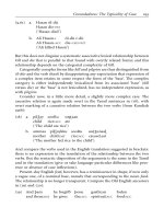
HK = −I(r − R(i) )sS (i) ,
(1)