DSpace at VNU: Preparation of transparent conducting Zno:Al films on glass substrates by r.f magnetron sputtering
Bạn đang xem bản rút gọn của tài liệu. Xem và tải ngay bản đầy đủ của tài liệu tại đây (1.03 MB, 6 trang )
VNU. JOURNAL OF SCIENCE, M athem atics - Physics. T .X V III, N02 - 2002
P R E P A R A T IO N
Z n O :A l
BY
r .f
O F T R A N S P A R E N T C O N D U C T IN G
F IL M S O N G L A S S S U B S T R A T E S
M AGNETRON
S P U T T E R IN G
N g u y e n D u y P h u o n g , T a D in h C a n h ,
N g u y e n N g u y e n N goc L ong, N g u y e n H o n g V ie t
D e p a rtm e n t o f P hysics, College o f S cien ce - V N U
Highly transparent, conducting y4/-doped Z n O films with good adherence anti low
resistivity have been prepared on glass substrates by r . f m agnetron sputtering. Mechan
ically stable polycrystalline conductive Z n O : A l films had a preferred orientation with
the (002) planes parallel to the substrate surface. The Z n O : A l films showed a resis
tivity in the range from 8.7 X 10"3 to 1.8 X 10~:*i2 cm, a carrier density in the range
(0.2 - 3.1) X 1020cm *3 and a Hall mobility between 7 and 17 cm2Vr-1 5“ 1. The average
transm ittance in the visible range exceeded 89 % for a 1.9ịim thick film. The films showed
a band-edge photoluminescence. The origin of the observed near-UV lines was identified
in terms of hound exciton complexes, bound electron with free hole recombination and
donor - acceptor pairs.
1. I n tr o d u c tio n
Transparent conducting zinc oxide films have been extensively studied ill recent
years, because of their low m aterial cost, relatively low deposition tem perature and s ta
bility ill hydrogen plasma compared to ITO and S n O 2 films [1]. These advantages arc of
considerable interest for solar energy conversion applications.
Z n O is a 7fc-type wide bandage semiconductor with w urtzite crystal structure. Noil'
stoichiometric undoped zinc oxide thin films have usually shown a low resist ivHy due to
oxygen vacancies and zinc interstitials [2]. Hence, low resistivity films can bo obtained by
controlling these native defects. Nevertheless, m any a tte m p ts have been made to reach
low resistivity by eloping with group-III elements such as alum inium [3], because it has
been remarked th a t extrinsic donors due to the dopant atom s are more stable than the
intrinsic donors due to the native defects. Comparing with undoped Z n O , A l - doped
Z n O films have lower resistivity and better stability. A decrease in resistivity resulting
from an increase in carrier concentration from 1020 to 1021 c m "3 was obtained as the
impurity content doped into the Z n O films increased Í4]. However, this increase ill carrier
concentration resulted in a decrease in mobility as well as optical transm it timer ill the
n e a r - I R ra n g e [5].
In this paper, the structural, optical and electrical properties of Z n O : A l films
prepared by r . f m agnetron sputtering have been investigated in detail, together with the
effects of heat treatm ent in air and hydrogen.
40
P re p a r a tio n o f tr a n sp a r e n t c o n d u c tin g Z tiO : Al fil m s on.
41
2. E x p e r im e n t
The films wen* deposited oil lass substrates by sputtering a 75 mm diam eter Z n ( ) :
A l target in a convontioiKil I'.f m agnetron sputtering system (Univox - 450 systom of
Lrybold Coorp.) with 10 L Ion basic pressure. A power supply operated at a crystal controlled frequency ol 13.56 MHz. The target with a m ixture of Z n O (99.9 c/i purity)
and A faO z (99.9 % purity) was employed as source material. The target was prepared by
using conventional sintering process. The content of A l 2 Ơ:\ added to the used target was 2
% in weight. The (listancr Ix'tw m i target and substrate was about 6 cm. The sputtering
gas A t with 99.9 % purity was controlled via a crystal controlled high frequency power
source. A heritor un
Controlled param eters vmT varied systematic ally ill order to obtain optim um qual
ity films (low resistivity, liiftli transmission and good adhesion to the substrates).
T h e following param otors were found to be suitable and were used in film prepara
tion: th e content of AloO:\ in the used target was 2w t.% . the input power was from 100 w
to 360 w a n d t h e A r p re s s u re w as 9 X 10~:* T o rr. U n d e r th o s e c o n d itio n s , thí* d e p o s itio n
rate was about 127/m mill 1
The sheet resistivities were» measured by a four - point probe instrum ent. The
thickness of the films was measured using a a-step X30 surface - profile' measured system.
The Hall measurement was made at room tem perature. The optical transm ittance mea
surement was performed with a ƯV-3001 spectrophotom eter. The structural properties
w
3. R e s u lts a n d d isc u ssio n
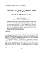
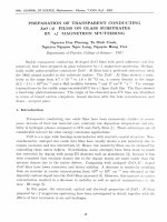
Fig. 1. SEM surface (a) and cross * section (b) m icrographs of a ZnO:Al film on glass
s u b s tra te a t r.f power 350 w and argon pressu re 8 .8 \tim e s l0 ‘3 Torr
A2Nguyen D u y P h u o n g , Ta D in h C a n h , N g u y e n N g o e L o n g , N g u y e n H ong V ie t
X-ray diffraction (XRD) spectra and SEM micrographs indicate th at the HIms grow
strongly textured in columnar structure with the hexagonal e-axis perpendicular to the
substrate surface. Typical SEM imagos are shown in F ig.l. When the columnar structure
appeared, the dom inant XRD peak was the (002) reflex at 34.4° (Fig. 2).
Fig. lb shows the vertical cross-sectional view of the Z n ( ) : A l film of nearly 2/rm
thick on glass substrate. The columnar growth of the film is clearly seen from rh<‘ figure;
that, is indicative of a strong oaxis orientation of the film. The SEM observation shows
also that the films deposited at low r . f powers exhibit a ’’toothed structure” on the top
layer with fine vertical line patterns (Fig. 3). The compactness of the coating increases
with the r . f power (Fig. la). Composition of the films was analyzed along surface by
energy dispersion spectrum (EDS) (Fig. 4). It is seen from the figure th at oxygen, zinc
and aluminium compositions in the films were rather alike distributed.
2-Theta-Scale
F ig . 2. X-ray diffraction p a tte rn of
ZnO:Al film deposited on glass
su b stra te
a
Fig. 3. SEM of ZnO:Al film deposited on
glass su b stra te a t r.f power 100 w and argon
pressu re 8.8 X 10‘3 Torr
Electrical measurements showed that
n
m
n
i
at room tem perature t he Z n O : A l films
showed a low resistivity value of (1.8 —
8.7) X 10~3ficm, a carrier concentration of
(0 .2 -3 .1 ) X 1020 cm ” 3 and a Hall mobility
of (7 - 17 )c m ? V ~ i s ~ l .
The transm ittance spectrum of a Z n O
A l film g ro w n a t r . f pow er 350 w a n d a r
gon p r e s s u re 8.8 X 10 “ 3 T o r r is p r e s e n te d
in Fig. 5. As can he seen from the figure,
Fig. 4. Com positions of ZnO:A]
average transm itance in the visible region
film s along surface
is about 89 %.
The optical absorption coefficient a can be described by the relation for parabolic
bands:
a h v = A ( h v - E g)1/N
(1)
p r e p a r a t i o n o f tra n sp a r e n t c o n d u c tin g Z n O : Al f il m s on.
43
w h ere A is thf‘ co n stan t. h i' is the ph oto n energy, Eg is the band Rap of the semiconductor.
V depends on tin*ty |><‘ <>i till1 (‘lection transition ' 6 !.
For (lin'd allowed transitions to an em pty parabolic conduction band N is to he
Srf't til 2
The rncr^Y l>;m
irnt pjvrn in E q.(l) versus the photon energy rurv<\ as ail insert ill Fig.
5. T h i' (‘S tim n tr d c n e i^ v b u n d grip Eg WHS 3.60 <‘V.
Wavelength (nm.)
F ig. 5. O ptical tran sm itta n ce of a ZnOrAl film deposited on glass u b stra te a t r.f power
35 0 w a n d a r g o n p r e s s u r e 8.8 X 10 1 T o r r .
PhotolumiuosnMico (PL) sjMTtra of Z n O : A l films were measured in the tem pera
ture range' from 11 K to room tem perature with excitation wavelength 300 mil Typical
PL spectra at 11 100. 270 K HIT shown in Fig. 6. The PL spectrum at 11 K exhibits
three «mission linos with maxima at 368 nm (3.368 eV), 374 mil (3.314 eV). and 384 nm
(3.228 cV). As can 1)0 s<‘(»n in the figure, the PL spectrum measured at 11 K is dominated
by emission lino at 368 run (Fig. 6a),
The intensity of PL linos (increases and their relative intensity changes with increas
ing temperature'. Th(* inim sity of the 368 U1Ì1 line fast decreases and at 50 K it can not
be observed, whilr the .’>71 mil line almost, does not change in position until 200 K. Above
200 K the 374 urn lino is broadened and slightly shifts to the long wavelength side and it
is located at 379 run (3.271 <'V) at 270 K. In contrast to the 374 run lino, the little broad
line peaked at 384 mil shifts to the long wavelength side with increasing tem pérature even
from 50 K and it is locritrcl at 407 mil (3.046 eV) at 100 K. at the tem peratures higher
than 150 K this line will he (Wtinct. Under such conditions a new emission line at 382 mil
(3.245 eV) can h r revealed (Fi&. 6b). At 270 K. in the PL spectrum the only emission
line located at 379 11111 can be observed (Fig. 6c)The 368 nm line cun he assigned to neutral-donor-bound-exciton (D°X) complexes;
the 374 11m lino is
AANguyen D u y P h u o n g , Ta D in h C a n h , N g u y e n N goe L o n g , N g u y e n H o n g V ie t
holes in valence band (BF). The energy separation between the 374 m il and 382 run linos
is 69 meV. which agrees well with the longitudinal optical phonon energy in Z n O . So.
the 382 nm line is regarded as a phonon replica of the 374 nm line (BF-LO). The broad
line at 407 nm can he interpreted as result of the donor - acceptor pairs (DAP) radiative
transitions.
Wavelength (nm.)
Fig. 6. PL spectra of ZnO:Al film s w ith excitạtion
w avelength 300 nm a t different tem p eratu res:
a) 11 K, b) 100 Kt c) 270 K
A c k n o w le d g e m e n ts. The authors would like to thank Center for Material Science.
Departm ent of Physics, College of Science - VNU, Hanoi for permission to use equipment
as well as National Program for Natural Science for financial support.
R e fe re n c e s
1. w .s . Lan. S.J. Fonash, J. E lectro n . M a ter., 16(1987), 141.
2. D.H. Zhang and D.E. Brodie, T h in Solid F ilm s , 238(1994), 95.
3. D.H. Zhang, T.L. Yang, J. Ma, Q.p. Wang, R .w . Gao, H.L. Ma, A pplied Surface
Science . 158(2000), 43 - 48.
P re p a r a tio n o f tra n sp a ren t c o n d u c tin g Z n O : Al f il m s o n ...
45
4. M.A. M artini'/. .Ỉ liciKTo. VI.T. Gntirrez. Solar E nergy M a teria ls a n d Solar Cells.
45(1997). 75 - 86.
5. H. Sato. T Millîimi. Y Tiiniura. s. Takata, T. Mouri and N Ogawa. Thin Solid
F ilm s , 246 ( m i ) . 8f> - i)l.
G. .J. Szcvrbowski. A. Dietrich and H. Hoffmann. Phys. S ta t. Sol., A 78(1983), 243.
TAP CHÍ KHOA HỌC ĐHQGHN, Toán - Lý, T XVIII, Số 2 - 2002
C H Ế TẠO M ẢNG BÁN DẪN TRONG SUỐT Z n O : A l TRÊN Đ Ế THƯ Ý TINH
B À N G PH U O N G PH Á P PH Ú N XẠ M A G N E T R O N
N g u y ề n D u y P hư cm g, T ạ Đ ìn h C ả n h
N guyền N gọc L o n g ,
Nguyễn
H ổĩìị» V iệ t
Khoa Vật ly. Dại học Khoa học T ự nhiên, ĐHQG Hủ Nội
M àng bán dẫn Z n () pha Al có độ truvén qua cao, độ bám dính tốt, diện trở thấp
đã được chê tạo trẽn đê thuV tinh bàng phương pháp phún xạ magnetron. Màng bán dẫn
Z n O : A I đa tinh thè có hướng ưu tiên với mặt (002) song song với bé mặt đế. Điện trờ của
các màng Z n ( ) : /1/ đà chế tạo nằm trong khong (1,8 - 8,7) X 10 'Qcm, nồng độ hạt tái
irong khoàns ( 0 ,2 - 3 , 1) X 102oc*m \ độ linh động Hall có giá trị nằm giữa 7 - 17c7n2V ~ l 8 ~ l .
f)ộ truyền qua trung hình của màne có độ dầy 1 ,9/Z//7 là 89 % trong miền nhìn thấy.