DSpace at VNU: Preparation of Pb(Zr, Ti)O3 thin films sputtered from a multi-element metallic target
Bạn đang xem bản rút gọn của tài liệu. Xem và tải ngay bản đầy đủ của tài liệu tại đây (281.36 KB, 6 trang )
VNU. j o u r n a l Of1 SCIENCE, Mathematics - Physics, T . x x , N01 - 2004
p r e p a r a t io n o f
Pb(Z r,T i)03 THIN FILMS SPUTTERED FROM
A MULTIELEM ENT METALLIC TARGET
N g u y e n T h a n h H u y a, Vu N goc H u n g a b, N g u y e n P h u T h u y a,c
ữ International Training Institute for Materials Science (ITIMS)
b Institute o f Engineering Physics, Hanoi University o f Technology
c F aculty o f Technology, Hanoi N ational University
Abstract: PZT thin films have been grown on Pt/Ti/Si02/Si substrates by the
reactive RF-magnetron sputtering deposition method using a multi-element
metallic target. The AB0 3 perovskite structure in the thin films sputtered at a
substrate temperature of 250 °c was formed through various intermediate
phases by annealing at 650 °c for 1 hour in the air or an oxygen gas ambience.
The film compositions were estimated by Electron Probe Micro-Analyzer
(EPMA). The surface morphology observed by Atomic Force Microscopy (AFM)
showed a densely packed grain structure with no rosettes structure. The
remanent polarization value of the thin film with a thickness of 500 nm was
1.37 nC/cm .
1. I n t r o d u c t io n
Over the last 20 years, thin films of lead zirconate titanate, Pb(Zr,Ti)03 (PZT),
have been attracted much attention due to their applications in nonvolatile memory
and MicroElectroMechanic Systems (MEMS) devices[l,2]. Most of works have been
concentrated on the compositions of the Morphotropic Phase Boundary (MPB) at
around Zr/Ti=50/50 compositional ratio, at which the piezoelectric and ferroelectric
properties show their maximum values. Various technical solutions proposed for
obtaining the thin films of PZT such as sol-gel method, pulsed laser ablation,
sputter deposition, and ion beam sputtering have been employed. Among them, the
sputtering method has been most widely used for obtaining high quality PZT films
because of its relatively simple fabrication process.
One of the most important factors in the preparation of PZT thin films is the
control of the correct perovskite phase formation in order to obtain the desired
electrical properties. Mostly, in the as-deposited films there have been no
perovskite phase. So post-deposition annealing treatments at high temperatures,
typically in the ra n g e 6 00-700 ° c for 1 hour or more, are necessary to crystallize the
film into perovskite structure.
In this study, PZT thin films were fabricated by the reactive RF-magnetron
sputtering method. The perovskite phase crystallization of PZT films was
investigated in term of the effects of annealing time and heat treatment ambience
by X-Ray Diffraction (XRD). The surface morphology and electrical properties ỔĨ the
films were also reported.
31
Nguyen Thanh Huy, Vu Ngoc Hung, Nguyen Phu Thuy
32
2. E x p e r im e n t a l p r o c e d u r e
An Alcatel SCM-400
13.56MHz RFm ag n etro n sp u tte rin g system was used to
deposit th e PZT th in film& on P t/T i/S i0 2/Si
m u ltip lay er
su b s tra te s .
During
sputterin g
process, the substrates, as bottom electrodes,
w ere h e a te d a t 250 ° c . T he s p u tte rin g ta r g e t w as
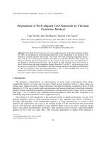
m ulti-elem ent m etallic, the design of which is
shown in Fig. 1. This was composed of individual
sectors of Pb, Zr, and Ti m etals with
Fig. 1. The multi-element
Pb/Zr/Ti:2/7.5/8.5 compositional ratio. Prior to
PZT m etal target (after
the deposition, the sp u tterin g cham ber was
sputtering)
pum ped down to a base pressure of 1 0 6 mbar.
Subsequently, gas m ixture of Ar and 0 2 with A r /0 2:60/40 ratio was introduced to a
p ressu re of 2 x l 0 '2 m bar. An RF-power was fixed at 200 w . The selected sp u tterin g
conditions for the deposition of bottom electrodes and PZT th in films are
su m m arize d in Table 1.
T a b le 1. T h e c o n d itio n s for p r e p a r a tio n of b ottom e le ctro d es a n d th e PZT(51/49)
th in films.
Bottom electrodes
200 w
RF- power
~ 10‘6 m bar
Base pressure
S ubstrate
T arget
P Z T thin film s
sitysi
Ti
Pt
Pt/T i/Si02/Si
Pb/Zr/Ti
W orking pressure
3x10 3 mbar
1x 10 2 m bar
Ambience gas
Ar
0 2/Ar:40/60
S u b strate tem perature TA Room
Deposition time
Film thickness
Ti: 5 min.
Pt: 30 min.
Ti: 20 nm.
Pt: 100 nm
250 °c
4 hours
500 nm
The PZT film th ickn ess was determ ined about 500 nm by the grazing incident
X-Ray Reflection (XRR), as illu stra te d in Fig. 2. The Zr/Ti:51/49 compositional ratio
of the PZT film s was analyzed using Electron Probe Micro-Analyzer (EPMA). In
order to crystallize perovskite phase, the as-deposited films were a n n ea le d using
Preparation of Pb(Zr, Ti)03 thin films sputtered from .
conventional furnace
at 650°c fixed
tem p era tu re in the a ir and an oxygen
ambience for 30, 60, 90, 120 min.,
respectively.
Phase
and
crystalline
behavior analyses of PZT films were
performed using X-Ray Diffractometer
with the CuKa source (A= 1.5405 A).
Surface morphology and grain size were
investigated
using
Atomic
Force
Microscopy (AFM).
The
ferroelectric
property of PZT thin films were also
m easured using RT 66 A standardized
hysteresis tester (R adiant Technology).
33
20 (deg.)
Fig. 2. The XRR p a tte rn of the PZT
thin film annealed at 650°c for 60
min
3. R e s u lts an d d i s c u s s i o n
C ry s ta llo g r a p h ic s tr u c t u r e
The crystal stru c tu re of the
as-deposited and an nealed PZT
thin films was exam ined by XRD
p a tte rn s
in
comparison
with
crystallographic
inform ation
reported earlier on PZT films and
ceramics. This p a rt may shed light
on th e optim um a nnealing time
and ambience required for the
perovskite PZT formation. The
XRD p a tte rn s of the films annealed
for th e various tim es in the air are
given in Fig. 3.
It can be seen from the figure
th a t all of films alw ays show two
peaks
at 2Ớ=40° and
46.55°
corresponding
to
the
Pt
polycrystalline phase.
• P erovskite
T =650c
□ P latinu m
* P
y ro c h lo re
ryiuuiiiuic
1
.« P b O
ss
•
^
-p
I
1
tn=
•7_ □
f\
120 mill.
•
>»
3
As-dcpositcd
20
30
40
2 0 (d c g .)
50
60
Fig. 3. The XRD p attern of PZT thin films
annealed for various annealing times
In case of the as-deposited
film, th ere are two peaks a t 29.6° and 34.15° depicting non-ferroelectric pyrochlore,
Pb,T i 20 6 cubic oxygen deficiency phase at low tem p era tu re . A p eak a t 56.24° is
identified ct-PbO, stru c tu re . Mean while it is possible th a t Z r 0 2, T i 0 2 a re presen ted
in a n am orphous form because whole Pb, Zr, Ti were oxidized in s p u tte rin g process
sim ultaneously.
34
Nguyen Thanh Huy , Vu Ngoc Hung , Nguyen Phu Th.uy
When the film was annealed for 30 min., a - P b 0 2 tra n s fe rre d to the lead-riich
phases PbOss t h a t are observed at 29 of 23.2°, 25.45°, 32.1°, an d 42.4°. Their relati ve
high intensity may show the excess contents of Pb and Oọ in the th in film[3]. T h e
peaks at 29.05° and 33.94° m atch with the pyrochlore monoclinic AB 3O 7 p h a se,
which is norm ally caused by a deficiency in lead due to an evaporation at hi;gh
tem peratu re. In th is work, the pyrochlore phase ap pears even when lead-rich PbOgg
compound presented in accordance with [4]. It has revealed th a t th e formation of
AB 30 7-type was favored over A B 0 3-type even when the Pb/Ti ratio was g reater th.an
one and AB3O7 phas e seemed to be an intermediate ph as e before the PZT fi lm s
crystallized into the ABO3 perovskite phase. The peaks at 21.75° and 38.55° perfoirm
the perovskite stru tu re . It is confirmed th a t the PZT films deposited at t h e
su b strate te m p e ra tu re 250°c can be converted into the perovskite crystalline
stru ctu re at the a nnealing te m p e ra tu re 650 °c with a sufficient a nn ealin g time.
Increasing the a nnealing time to 60 min., complete perovskite crystallization
occurs. Besides the form er peaks, the others at 30.77°, 44.15°, and 54.85° according
to the perovskite phase appears. The ratio of intensity betw een the peaks show t h a t
the stru c tu re of the PZT th in film is polycrystalline (like PZT ceramic)[5]. However,
the (110) intensity peak at 30.77° is largely superior to the others, thus it is
considered th a t the th in films has a preferred-(llO ) orientation.
The tren d suggests th a t these films may be converted into the single
perovskite phase by increasing the annealing time or a n n ealin g tem p era tu re .
■Nevertheless, the annealed films for more th a n 60 min. are diphase w ith pyrochlore
and perovskite coexistence. The pyrochlore peaks re a p p e a r t h a t proves Pb loss. T he
deficiency of Pb is u n d e rstan d a b le by considering its high volatility for a long
annealing time at a high tem p era tu re . After the annealing tim e reaching 120 min.,
the non-ferroelectric pyrochlore phase is predom inating with strong and sh a rp
peaks.
To investigate the effect of annealing ambiences, the PZT th in films were
annealed for 60 min. a t 650 °c in the air, an oxygen and an argon gas ambience and
the results are depicted in Fig. 4. As above discussion, the thin film, which was
heated in the air, has the polycrystalline perovskite s tru c tu re with predom inated
(110) orientation. The film annealed in the oxygen ambience has still the correct
perovskite. stru c tu re b u t (100) orientation is preferred. It may be caused by the
influence'of oxygen content on PZT orientations. It has been reported th a t the
oxygen partial pressu re is an im p o rtan t factor in determ inin g the Pb valence sta te
in th e PZT film s, w hich d ic ta te s th e k in e tic s of th e p y ro ch lo re-p ero v sk ite p h ase
transformation^]. A low Pb valency state enhances the kinetics of transformation,
whereas a high Pb valence state suppresses the kinetics of tran sfo rm a tio n leading
to incomplete tran sfo rm a tio n of the pyrochlore to perovskite phase. The growth of
PZT(100) on P t/T i/S i0 2/Si wafers a ttrib u te d to the form ation of crystalline PbO(OOl)
P r e p a r a t ° n ° f Pb(Zr, Ti)03 thin films sputtered from .
d u rin g p rolysis. PbO has good
lattice notching w ith PZT(IOO)
orientatioi;
this
lowers
the
in terfacia energy and promotes
the nucliation of PZT(IOO). On
the contiiry, for the PZT film
a n n e a le d in the argon ambience
the pyro
35
• P ero v sk ite
□ P latinum
□
❖P y ro ch lo re
-P
T h e air
*C/5
3
.. .
O x y g e n gas
complete}/.
Altlough PZT films were
A rg o n gas
ẳ I 111 I I ẵ ẫ1 I i I I ẳ
an n ea le d for different tim es in
6C
50
40
20
to
various anbiences, the ( 110 ) or
20 (deg.)
( 100 )
o’ientation
is
mainly
observed. These resu lts imply
Fig. 4. The XRD p attern of PZT thin films
annealed in various annealing ambiences.
th a t PZT essentially has n a tu ra l
preference to grow in ( 110 ) or
( 100 ) directions at te m p e ra tu re s less th a n 700 °C[7].
On he basic of this information, the crystallization of sp u tte rd PZT th in films
was studied. The as-deposited film shows peaks due to a - P b 0 2 and A 2B 20 7.x
crystalline while Z r 0 2 and T i 0 2 are amorphous. After annealing, lead-rich PbOss
and lead deficient AB 30 7 phases were found as the in te rm e d iate phases and they
reacted each other to form the perovskite stru c tu re during post-deposition heat
treatm ents. In order to obtain the correct perovskite crystal s tru c tu re the PZT thin
films need to be a nn ealed for 60 mill, at 650 °c in the a ir or the oxygen ambience.
S u r fa c e m orp h o lo g y a n d g r a i n size
100 urn
The
surface
morphological
investigation on the sp u ttere d PZT thin
film annealed at 650 °c for 60 min. in the
air was shown in Fig. 5. The film has a
relative
smooth
surface
with
no
microcrack, a dense stru c tu re , and fine
grain.distributing homogeneous. Agreeing
well with AFM result, the average grain
size is also estim ated to be 50 nm by
using S h e rre r’s equation with the half
width of the ( 110 ) diffractive peak
observed at 2Ớ=30.77° in the XRD p attern
in Fig. 4.
50
Í
m il
Ọ IU11
2 11I I I
Fig. 5. The AFM micrograph of PZT thin
film annealed at 650°c for 60 min. in the
air
Nguyen Thanh Huy, Vu Ngoc Hung , Nguyen Phu Thuy
36
F erro ele ctric p r o p e r ty
Ferroelectric behavior of the PZT film a n n e a le d -a t 650 °c for 60 min. in th e
air was stu d ied by a p lotting P-E h y steresis loop and is show n in Fig. 6 .
The re m e n a n t polarization P r of the
PZT film is about 1.37. |iC/cm 2. The film
exhibits
th e
c h a ra c teristic
“elliptic”
shaped ferroelectric response of a h ard
ferroelectric. This shape is common for
film referred to as “lossy” or “leaky”,
which is not good in su lato r. The loop has
shifted tow ard the negative side. This
asym m etry also observed by m any
workers w as a ttrib u te d to the difference
in
in terfacial
sta te s
betw een
top
electrode/PZT interface and PZT/bottom
electrode in te rfa c e [8 ] due to the electrodes
were p rep ared in com pletely different
conditions.
4.
V (Volt)
Fig. 6 . The P-E p a tte rn of the PZT th in
film at 650 °c for 60 min. in the air
C o n c lu s io n s
PZT th in film s were p repared on platinized silicon s u b s tra te s
by RFm agnetron sp u tte rin g m ethod using a m ulti-elem ent m etallic targ e t. Lead-rich
P b 0 8s and lead-deficient AB 3O 7 phases were discussed as im m ed iate phases in th e
ABO;i correct perovskite crystallization. The com plete perovskite stru c tu re could be
obtained a t the optim ized condition being a t 650 °c an n ealed te m p e ra tu re for 60
min. in the a ir or the oxygen am bience.
References
1.
J. F. Scott and c . A. Paz de Araujo, Science. 246(1989),1400.
2.
E. Defay, c . Millon, c . Malhaire, D. Barbier, Sensors and Actuators, 99(2002), 64.
3.
S. M. Ha, D. H. Kim and H. H. P ark, Thin Solid Films, 355-356 (1999), 525.
4.
c . V. R. V asan t K um ar and R. Pascual, J. Appl. Phys., 71(1992), 864.
5.
D. Czekaj, M. J. M. Gomes, M. V asilevskiy and M. P eira, J. Euro. Ceram. Soc,.
19(1999), 1489.
6.
S. K alpat and K. Uchino, J. Appl. Phys., 90(2001), 2703.
7.
K. Iijim a, Jpn. J. Appl. Phys. 30 (9)(1991), 2149.
8.
S. O kam ura, s . M iyata and Y. M izutani, Jpn. J. Appl. Phys. 38 (1999) 5364.