DSpace at VNU: Effect of BaSnO3 Nanoparticle Inclusion on Critical Current Density of GdBa2Cu3O7- Thin Films
Bạn đang xem bản rút gọn của tài liệu. Xem và tải ngay bản đầy đủ của tài liệu tại đây (354.14 KB, 6 trang )
VNU Journal of Mathematics – Physics, Vol. 29, No. 3 (2013) 49-54
Effect of BaSnO3 Nanoparticle Inclusion on Critical Current
Density of GdBa2Cu3O7-δ Thin Films
Duong Thi Thanh Nhan1,*, Tran Hai Duc2
1
VNU University of Science, 334 Nguyen Trai, Hanoi, Vietnam
2
Chungbuk National University, Cheongju, Korea
Received 12 August 2013
Revised 30 August 2013; Accepted 09 September 2013
Abstract: Effect of BaSnO3 (BSO) nanoparticle inclusion on the critical current density of
GdBa2Cu3O7-x (GdBCO) thin films was investigated. BSO nanoparticles were prepared on a thin
GdBCO seed layer of < 50 nm thick by using pulsed laser deposition (PLD) technique. The
GdBCO superconducting layers were deposited on top of the BSO nanoparticles to produce films
with the entire thickness of approximately 250 nm. The number of laser pulses was varied from 20
to 320 in order to obtain BSO nanoparticles with different sizes and densities. Magnetization data
measured at 65 K showed that: at a small number of laser pulses, the slight enhancement in critical
current density (Jc) up to 1.5 T was obtained. Further increasing the number of laser pulses, Jcs
were found to be consistently decreased. The increase in Jc was attributed to the addition of BSO
nanoparticles serving as artificial pinning centers (APCs) inside GdBCO films. The decreases in Jc
was probably caused by to the crystallinity degradation of the BSO-doped GdBCO films which
was confirmed by the larger FHWM values.
Keywords: GdBCO thin film, critical current density, BaSnO3, artificial pinning centers.
1. Introduction*
REBa2Cu3O7-δ (RE: rare earth)-coated conductors have been reported to have superior field
performances than those of standard YBa2Cu3O7-δ (YBCO). Substitution of Gd for Y has been shown
to induce the enhanced critical temperature (Tc) which resulted in higher irreversibility field (Hirr) and
a critical current density (Jc) at 65 K and 77 K [1-3] . For power applications of the second generation
of high temperature superconductors, GdBCO has been considered as one of the most promising
candidate.
Applications of GdBCO-coated conductors (CCs) require them to be exposed to high fields. Their
in-field Jc is determined by the flux-pinning effect which is arisen from defects in the crystal structures
_______
*
Corresponding author. Tel.: 84-1293999129
Email:
49
50
D.T.T. Nhan, T.H. Duc / VNU Journal of Mathematics-Physics, Vol. 29, No. 3 (2013) 49-54
of GdBCO such as dislocations, grain boundaries, or fine precipitates, and these defects have been
found to serve as pinning centers [4]. However, the in-field Jc at 65 K and 77 K is drastically
decreased. In order to improve the Jc of GdBCO (or REBCO), different nanoengineering techniques
have been developed for introducing and controlling artificial pinning centers (APCs) into the films
[4]. One of the most common techniques that satisfy the condition of easily controlled properties of
the APCs is the deposition of nanoparticles in which the properties consisting of the average size and
density of the nanoparticles are varied by changing the ablation laser pulses.
In this paper, we study the effect of BSO nanoparticle dispersions on the critical current density in
the GdBCO thin films. BSO was selected as a dopant material because our previous study had shown
that BSO provides the significant Jc improvement via the formation of a BSO nano precipitate [5]. The
introduction of the BSO nanoparticles into GdBCO films was carried out by using two separate
targets, GdBCO and BSO those were made from the solid state reacted methods. From the
microstructural characterizations, the BSO nanoparticle dispersions were found to be located on the
GdBCO buffer layer with a distance of ~ 50 nm from film/substrate interface. The field dependence of
the Jc data showed that Jc enhancements were obtained for the GdBCO with a dilute doping of BSO
nanoparticles.
2. Experiment
The GdBCO thin films with and without the BSO nanoparticle inclusions were deposited on
SrTiO3 (STO) single crystalline substrates by separately ablating the two solid-state reacted targets of
GdBCO and BSO. The film structure was designed to consist of the two GdBCO layers sandwiched
by a BSO pseudo-layer. For GdBCO phase, an energy of 250 mJ and a repetition rate of 8 Hz was
used. The first GdBCO layer with a thickness of ~ 50 nm was functioned as a buffer layer for growing
BSO nanoparticles. The preparation of BSO nanoparticles on an approximately 50-nm-thick GdBCO
buffer layers were performed at a lower energy of 200 mJ with a number of laser pulses varied from
20 to 320. The entire film thickness was maintained at ~ 250 nm. All depositions were carried out at a
substrate temperature of 780oC and an oxygen pressure of 150 mTorr. After the depositions, all films
were annealed at 500oC in 500 Torr of oxygen for 1 hour and then were freely cooled to room
temperature.
The crystalline structure and texture of GdBCO films were examined by using an X-ray θ-2θ and
ω diffractometer with a Cu Kα radiation. The BSO nanoparticle inclusions on a GdBCO buffer layer
were observed by using atomic force microscopy (AFM). Cross-sectional scanning electron
microscopy (SEM) was employed to characterize the microstructures of the BSO-added GdBCO
films. The Jc values of the GdBCO films in magnetic fields applied perpendicular to the film normal
were derived from the magnetization data measured by using the magnetic properties measurement
system (MPMS) XL-5 SQUID magnetometer.
D.T.T. Nhan, T.H. Duc / VNU Journal of Mathematics-Physics, No. 29, No. 3 (2013) 49-54
51
3. Results and discussion
The preparations of BSO nanoparticles on GdBCO buffer layers that had been deposited on STO
substrates by using 20-320 laser pulses. The optimum condition for the impurity nanoparticles to work
as APCs has been reported to be the substrate surface decoration. The nanoparticles grown on the bare
substrates were observed to induce the dislocation-like defects with some of them thoroughly extended
to the top film surface. We have completely done that kind of research using the Gd2O3 nanoparticles
[6]. With the aim to search another candidate for APCs, we moved to BSO-a perovskite structurewhich has been studied to be chemically stable with the REBCO superconductors. The growth of BSO
nanoparticles, however, could not be carried out on the bare substrates. Motivated from that point, a
thin GdBCO buffer layer was prepared as a basement for BSO.
Figures 1(a) and (b) exhibit two representative AFM images BSO nanoparticle inclusions
deposited by 20 and 320 laser pulses, respectively. Randomly-distributed BSO nanoparticles were
observed on the GdBCO buffer layer with BSO deposition. Detailed properties of the BSO
nanoparticles with respect to the number of laser pulses were automatically analyzed by using the
software equipped with AFM system. The resuts are listed in the Table. 1.
Table1. Properties of the BSO nanoparticles with respect to the number of laser pulses
Pulses
20
80
160
320
Mean diameter (nm)
17.6
26.8
30.2
38.2
Mean height (nm)
0.6
1.1
1.6
2.1
Density (µm-2)
62
11.4
163
183
Matching field (T)
0.128
0.235
0.337
0.378
The density of BSO particles increased monotonically from ~ 62 to 183 µm-2 with increasing
number of laser pulses from 20 to 320. In addition, the particles tended to coalesce as the number of
the pulses was increased, and as a result, the mean diameter of the BSO particles increased. Nanoscale
diameter of < 20 nm was obtained for the BSO particles deposited with 20 pulses only; this diameter
was comparable to other reports [7, 8]. Using 160 and 320-pulse BSO depositions, the values of the
mean diameters became relatively larger, 30.2 and 38.2 nm, respectively. The influences of the BSO
particles on the structural and the Jc of GdBCO thin films will be discussed below.
Figure 1. AFM images of BSO nanoparticles deposited on GdBCO buffer layer
with 20 (left) and with 320 (right) pulses.
52
D.T.T. Nhan, T.H. Duc / VNU Journal of Mathematics-Physics, Vol. 29, No. 3 (2013) 49-54
The BSO nanoparticles were first characterized by using AFM, then covered by the GdBCO
superconducting phase. In other words, the BSO nanoparticles were preserved inside the GdBCO film.
The effect of the BSO nanoparticle inclusions on the Jc was analyzed by using magnetization
measurements in a magnetic field applied parallel to the film normal. The calculations of Jc values
were done by using the simplified Bean’s model: Jc = 20∆M/[b(1-b/3a)] [9] where ∆M was the
magnetization difference per unit volume, and a and b were, respectively, the length and width of
samples, respectively. The field dependences of the Jc for GdBCO films with and without BSO
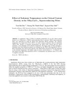
nanoparticle inclusions are exhibited in Figure 2.
GdBCO
20 pulses
80 pulses
160 pulses
320 pulses
7
2
JC (A/cm )
10
6
10
65 K
5
10
0
1
2
H(T)
3
4
Figure 2. Field dependences of the GdBCO thin films with and without the BSO nanoparticle inclusions. The Jc
enhancement was obtained for 20 pulses of the BSO deposition only, which suggested the effect of diluted BSO
doping. The decreases in Jc for higher numbers of laser pulses of the BSO deposition might be involved in the
changes in the film microstructures.
With the multilayer-like structure of the film in which the negligible change in the thicknesses of
the GdBCO buffer layer and GdBCO films, we are focusing on any change in Jc with respect to the
BSO nanoparticles. Self-field Jc’s of ~ 106 A/cm2 were estimated. Jc values of the GdBCO films with
BSO addition using 20 laser pulses of BSO deposition were found to slightly enhanced, compared to
that of the GdBCO film without the BSO addition. The relatively small enhancement in the Jc values
was corresponded to the low BSO particle density listed in Table 1. The magnetic flux pinning by a
second phase dispersion is most effective as the defect size is comparable to 2ξ, where ξ is coherence
length of GdBCO [9]. In addition, the low density of the BSO nanoparticles also prepared a large area
for the GdBCO superconducting phase. As a result, the Jc enhancement was induced.
Even though the small sizes and increased particles densities were given as increasing the number
of laser pulses, the Jc enhancement was disappeared. Instead, the Jc values of the GdBCO with BSO
addition using 80-320 pulses were observed to be consistently decreased. The formation of BSO
nanoparticle inclusion was still observed with the nanoscale sizes but its effectiveness was reduced,
which suggested another involved factors. As far as we know, the superconducting properties of the
HTS are closely correlated to their microstructural properties. In order to have the enhanced Jc’s along
D.T.T. Nhan, T.H. Duc / VNU Journal of Mathematics-Physics, No. 29, No. 3 (2013) 49-54
53
the ab plane of the GdBCO film, the crystal structure of the GdBCO film are required to be highly caxis oriented. The applied currents will probably flow in the CuO2 superconducting plane of GdBCO
the double-perovskite structure with the minimal dissipation. If the GdBCO films are highly c-axis
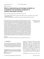
oriented, the ab // CuO2 planes will be provided for the current flowing. The ω-scan XRD rocking
curves of (005) reflection of the BSO-added GdBCO films were measured to examine changes in the
crystal structures of the GdBCO films with the additions of BSO.
GdBCO
80 pulses
320 pulses
8
6
4
Intensity (x10 arb.unit)
10
4
2
0
17
18
19
o
20
21
ω( )
Figure 3. ω -scan XRD rocking curves of (005) reflection of BSO doped GdBCO deposited by using separated
targets present that the out-of-plane texture is getting degraded with increasing number of laser pulses for
BSO depositions.
From the results illustrated in Figure. 3, it could be said that the values of FHWM increased from
0.44o (pure GdBCO) to 0.82o (80 pulses) and to 1.30o (320 pulses). The higher the FHWM was, the
higher the crystallinity degradation was. The larger numbers of the laser pulses might create the dense
pseudo-layers, which reduced the crystallinity of the GdBCO films. The formation of the BSO pseudolayer was observed by using the cross-sectional SEM images as shown in Figure 4.
Figure 4. Cross sectional SEM images of the GdBCO film for the 320 pulses of the BSO deposition. The BSO
nanoparticles were observed to be located ~ 30 nm near the film/substrate interface.
54
D.T.T. Nhan, T.H. Duc / VNU Journal of Mathematics-Physics, Vol. 29, No. 3 (2013) 49-54
4. Conclusions
We have studied the critical current density Jc of GdBCO thin films through a systematic addition
of BSO nanoparticles, leading to BSO nanoparticle inclusions. The BSO nanoparticles were prepared
on a GdBCO buffer layer by using the PLD technique before the GdBCO film deposition. The
diameter and density of BSO nanoparticles were controlled by varying the number of laser pulses from
20 to 320 pulses. Jc enhancement was obtained for 20 pulses of BSO deposition, suggesting that
effective pinning is obtainable in dilute BSO addition. Decreases in Jc were observed for higher
number of laser pulses of BSO deposition, which might be explained by the crystallinity degradations
of the BSO-added GdBCO films, which was confirmed by the cross-sectional SEM analysis.
5. References
[1] Y. Xu, M. Izumi, K. Tsuzuki, Y. Zhang, C. Xu, M. Murakami, N. Sakai and I. Hirabayashi, Thickness
dependence of critical current density in GdBa2Cu3O7−δ thin films with BaSnO3 addition, Supercond. Sci.
Technol, 22, 095009, (2009).
[2] S. Rosenzweig, J. Hänisch, K. Iida, A. Kauffmann, Ch. Mickel, T. Thersleff, J. Freudenberger, R. Hühne, B.
Holzapfel and L. Schultz, Thickness dependence of critical current density in GdBa2Cu3O7−δ thin films with
BaSnO3 addition, Supercond. Sci. Technol, 23, 105017, (2010).
[3] M. Murakami, N. Sakai, T. Higuchi and S.I. Yoo, Melt-processed light rare earth element-Ba-Cu-O Supercond.
Sci. Technol, 9, 1015 (1996).
[4] K. Matsumoto and P. Mele, Artificial pinning center technology to enhance vortex pinning in YBCO coated
conductors, Supercond. Sci. Technol, 23, 014001 (2010).
[5] D.H. Tran, W.B.K. Putri, C.H. Wie, B. Kang, N.H. Lee, W.N. Kang, J.Y. Lee, and W.K. Seong, Thickness
dependence of critical current density in GdBa2Cu3O7−δ thin films with BaSnO3 addition, J. Appl. Phys, 111,
07D714 (2012).
[6] D.H. Tran, W.B.K. Putri, C.H. Wie, B. Kang, N.H. Lee, W.N. Kang, J.Y. Lee and W.K. Seong, Enhanced critical
current density in GdBa2Cu3O7-δ thin films with substrate surface decoration using Gd2O3 nanoparticles ", Thin
Solid Films 526, 241 (2012).
[7] P. Mele, K. Matsumoto, T. Horide, O. Miura, A. Ichinose, M. Mukaida, Y. Yoshita, and S. Horii, Control of
Y2O3 nanoislands deposition parameters in order to induce defects formation and its influence on the critical
current density of YBCO films, Physica C, 426-431, 1108 (2005).
[8] P. Mikheenko, A. Sarkar, V.S. Dang, J.L. Tanner, J.S.Abell, and A. Crisan, c-Axis correlated extended defects
and critical current in YBa2Cu3Ox films grown on Au and Ag-nano dot decorated substrates, Physica C, 469, 798
(2009).
[9] P. N. Barnes, T. J. Haugan, C. V. Varanasi and T. A. Campbell, Flux pinning behavior of incomplete
multilayered lattice structures in YBa2Cu3O7−d, Appl. Phys. Lett, 85, 4088 (2004).
_______