DSpace at VNU: Influence of CoFe and NiFe pinned layers on sensitivity of planar Hall biosensors based on spin-valve structures
Bạn đang xem bản rút gọn của tài liệu. Xem và tải ngay bản đầy đủ của tài liệu tại đây (329.23 KB, 5 trang )
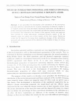
Home
Search
Collections
Journals
About
Contact us
My IOPscience
Influence of CoFe and NiFe pinned layers on sensitivity of planar Hall biosensors based on
spin-valve structures
This content has been downloaded from IOPscience. Please scroll down to see the full text.
2012 Adv. Nat. Sci: Nanosci. Nanotechnol. 3 045019
( />View the table of contents for this issue, or go to the journal homepage for more
Download details:
IP Address: 198.91.37.2
This content was downloaded on 21/02/2015 at 15:19
Please note that terms and conditions apply.
IOP PUBLISHING
ADVANCES IN NATURAL SCIENCES: NANOSCIENCE AND NANOTECHNOLOGY
Adv. Nat. Sci.: Nanosci. Nanotechnol. 3 (2012) 045019 (4pp)
doi:10.1088/2043-6262/3/4/045019
Influence of CoFe and NiFe pinned layers
on sensitivity of planar Hall biosensors
based on spin-valve structures
Dinh Tu Bui1 , Mau Danh Tran1 , Huu Duc Nguyen1,2
and Hai Binh Nguyen3
1
Department of Nano Magnetic Materials and Devices, University of Engineering and Technology,
Vietnam National University in Hanoi, 144 Xuan Thuy Road, Hanoi, Vietnam
2
Laboratory for Micro and Nano Technology, University of Engineering and Technology,
Vietnam National University in Hanoi, 144 Xuan Thuy Road, Hanoi, Vietnam
3
Institute of Materials Science, Vietnam Academy of Science and Technology 18 Hoang Quoc Viet
Road, Hanoi, Vietnam
E-mail:
Received 7 September 2012
Accepted for publication 11 October 2012
Published 7 December 2012
Online at stacks.iop.org/ANSN/3/045019
Abstract
This paper deals with the magnetization, magnetoresistance and planar Hall effect (PHE) of
NiFe(10)/Cu(1.2)/NiFe(tp )/IrMn(15) (nm) and NiFe(10)/Cu(1.2)/CoFe(tp )/IrMn(15) (nm)
spin-valve structures with various thicknesses of pinned layer tp = 2, 6, 9, 12 nm and a fixed
free layer NiFe of tf = 10 nm. Experimental investigations are performed for 50 × 50 µm
junctions fabricated using lithography technique. The results show that the thinner the pinned
layers, the higher is the PHE sensitivity obtained in both systems. In addition, in the spin-valve
structures with the same pinned layer thickness, the CoFe-based system exhibits higher
magnetoresistive ratio, but lower PHE sensitivity with respect to those of the FeNi-based
system. The results are discussed in terms of the spin twist as well as the coherent rotation of
the magnetization in the individual ferromagnetic layers. The highest PHE sensitivity S of
110 µV (kA m−1 )−1 has been obtained in the FeNi-based spin-valve structure with tp = 2 nm.
This result is rather promising for the spintronic biochip developments.
Keywords: planar Hall effect, Hall sensor, magnetic sensor, biochip, bead array counter
microchip
Classification numbers: 2.00, 4.00, 4.10, 5.00, 5.02, 6.09, 6.10
layer with uniaxial anisotropy can be rotated freely by a
small applied magnetic field in the film plane, while the
magnetization of the other magnetic layer has unidirectional
anisotropy pinned by exchange bias coupling from the AFM
layer. Recently, this effect has been well developed for
biochip applications due to its large resistance change in small
magnetic field range [5–11]. The GMR effect is related to
the switching of magnetic domain. It has low signal-to-noise
ratio (SNR), leading to a high error in detections of the
small stray field. The planar Hall effect (PHE), however,
is related to the rotation process of magnetic domain and
originates as the anisotropic magnetoresistance. This effect
exhibits a nano-tesla sensitivity and rather high SNR, so
1. Introduction
The spin valve, which was known as a simple embodiment
of the giant magnetoresistance (GMR) effect, was first
termed by Dieny et al [1] and has recently played a
key role in high-density magnetic recording heads and
magnetic biosensor due to their high magnetoresistance (MR)
ratio in low field and linear MR response [2–4]. Its
structure typically consists of two ferromagnetic (FM) layers
separated by a nonmagnetic conductor whose thickness is
smaller than the mean-free path of electrons. The magnetic
layers are uncoupled or weakly coupled in contrast to the
generally strong antiferromagnetic (AFM) state interaction
in Fe–Cr-like multilayer; thus the magnetization of an FM
2043-6262/12/045019+04$33.00
1
© 2012 Vietnam Academy of Science & Technology
Adv. Nat. Sci.: Nanosci. Nanotechnol. 3 (2012) 045019
D T Bui et al
it has received great attention for magnetic bead detections
and biosensor designs [5–8, 12, 13]. The transverse voltage
on a planar Hall cross depends on the orientation of the
magnetization in the ferromagnetic layer with respect to the
longitudinal sensing current. Thus, a large PHE is expected
to be observed in the exchange coupling based structures
because they can ensure a sufficient uniaxial anisotropy with
well-defined single domain state to introduce a unidirectional
anisotropy. Recently, Nguyen et al [10] have found that the
sensor signal can be further improved by using spin-valve
structure of NiFe(6)/Cu(3.5)/NiFe(3)/IrMn(10) (nm) in the
dimension of 3 × 3 µm when detecting the 2.8 µm magnetic
beads. Through our recent research, we see that spin-valve
structure with thickness of the Cu layer being 1.2 nm is
better [14]. The present paper deals with the influence of
pinned ferromagnetic layers on magnetic field sensitivity of
PHE sensors based on spin-valve structures. This has been
realized in NiFe(10)/Cu(1.2)/NiFe(tp )/IrMn(15) (nm) and
NiFe(10)/Cu(1.2)/CoFe(tp )/IrMn(15) (nm) structures with
various thicknesses of pinned layer tp = 2, 6, 9, 12 nm and
a fixed free layer NiFe of tf = 10 nm. The objective of this
study is to optimize the spin-valve structure for magnetic bead
detections.
(a)
Hy
Hx
Ix
(b)
2. Experimental procedures
The thin films with typical spin-valve structure of Ta(5)/
NiFe(10)/Cu(1.2)/NiFe(tP )/IrMn(15)/Ta(5) (nm) and
NiFe(10)/Cu(1.2)/CoFe(tp)/IrMn(15) (nm) with free
ferromagnetic (FFM) layer thicknesses tp = 2, 6, 9, 12 nm
and pinned ferromagnetic (PFM) layer thickness NiFe of
tf = 10 nm are fabricated by using magnetron sputtering
system with the base pressure less than 3 × 10⁻⁷ mTorr. The
spin-valve structures were sputtered on SiO2 wafer at room
temperature with Ar working pressure of 3 × 10⁻³ mTorr.
During the sputtering process, a uniform magnetic field of
Hx = 32000 A m−1 was applied in the plane parallel to the
Ox-direction of the films. This magnetic field induces a
magnetic anisotropy in the FFM and PFM layers and then
aligns the pinning direction of the AFM IrMn layer. The PHE
sensors were structured by using photolithography technique
into four-electrode bars with the patterned size of 50 × 50 µm
(figure 1(a)). The sensors were passivated by sputtering a
150 nm thick Si3 N4 layer to protect against the fluid used
during the experimentation. The bead array counter (BARC)
microchip was fabricated by integrating ten single sensor
patterns as shown in figure 1(b).
The PHE characteristics of sensors were measured at
room temperature by using a nanovoltmeter in the external
magnetic fields Hy up to 4 kA m−1 applied along Oy
direction and sensing currents Ix of 1 mA. Longitudinal
magneto-resistance was measured by means of a collinear
four-point probe method for samples with the size of
2 × 10 mm in magnetic field and sensing current applied
along Ox-direction. Magnetization was measured by using a
Lakeshore 7400 vibrating sample magnetometer.
Figure 1. (a) Top view micrograph of the single 50 µm ×50 µm
planar Hall resistance (PHR) cross. The pinning direction Hx as
well as the direction of the bias field Hy and sensing current Ix are
indicated. (b) The BARC including ten of single PHE sensors (with
eight single sensors in the two middle lines and one single sensor in
each edge line).
(nm) called sample 1 and Ta(5)/NiFe(10)/Cu(1.2)/NiFe(2)/
IrMn(15)/Ta(5) (nm) called sample 2. It is clearly seen that
all samples exhibit two hysteresis loops corresponding to
the magnetization processes of the FFM and PFM layers.
Magnetic reversed process of the sample 2 starts and
finishes sooner than that of sample 1. For sample 2, it starts
from magnetic field value of 700 A m−1 and final parallel
configuration of individual layer magnetization seems to be
completed at the magnetic field of Hf = 540 A m−1 . Whereas,
for sample 1, these parameters are 210 and 610 A m−1 ,
respectively. The PFM layer is expected to dominate the
sensor response at low magnetic fields. The values of the
coercivity (Hc ) and exchange coupling (Hex ) [14] fields
determined from the first hysteresis loop are listed in table 1.
There is a clear difference in values of Hc and Hex between
structures having the pinned layers CoFe and NiFe. The
difference is explained by exchange coupled field between
the pinned layer and the free layer via the Cu non-magnetic
layer. This field between the CoFe and NiFe layers is larger
than that between the NiFe and NiFe layers.
Shown in figure 3 are the PHE voltage profiles of both
of samples, VPHE , as a function of the applied field. Firstly,
the PHE voltage initially develops rather fast at low fields
reaching a maximal value at H < 1100 A m−1 for the sample
1 and H < 3000 A m−1 for the sample 2 and finally decreases
with further increasing of the magnetic fields. It is interesting
to note that the sensor sensitivity S(= dV /dH , see below) of
3. Results and discussion
Figure 2 presents the magnetization data of spin-valve
structures Ta(5)/NiFe(10)/Cu(1.2)/CoFe(2)/IrMn(15)/Ta(5)
2
Adv. Nat. Sci.: Nanosci. Nanotechnol. 3 (2012) 045019
D T Bui et al
Table 1. Values of sensor sensitivity (S), coercive (Hc ), anisotropy (Hk ), exchange coupling (Hex ) fields for spin-valve system with different
pinned layer.
Pinned layer
TP (nm)
S (µV kA−1 m)
Hc (A m−1 )
Hk (A m−1 )
Hex (A m−1 )
CoFe
NiFe
2
2
27
68.0
140
70
1000
230
3000
1140
Figure 4. Effect of thickness of the CoFe and NiFe pinned layer on
PHE sensor sensitivity S.
Figure 2. Magnetic hysteresis loops data of spin-valve structures of
samples 1 and 2.
the magnetization is pinned in different directions from the
easy axis (i.e. θP = 0) [16]. In this context, the twisted part
can be assumed to be eliminated in the structure with thin
pinned layer tP 2 nm [14]. Practically, the maximal PHE
voltage and the highest sensitivity of sensor were observed
in this configuration. For the thinner and softer (NiFe) PFM
layers, the magnetic influence and then the twist part can be
established near NM/FFM interface only. Thus it enhances the
PHE voltage.
Inversely, with the PFM layer having thicker and harder
(CoFe) layers, the twist part will be developed so the rotation
of the magnetization in the FFM is more difficult. Therefore,
PHE voltage is smaller. This is shown in figure 4.
Here, the most interesting result is that while the
maximum PHE voltage of sample 1 is 50 µV at H ∼
3000 A m−1 with sensitivity 27 µV (kA m−1 ), then sample 2
reaches the maximum PHE voltage value about 62 µV at
H ∼ 1100 A m−1 and this spin-valve configuration shows a
sensor sensitivity as large as 68 µV (kA m−1 )−1 .
Figure 3. Low field PHE profiles measured in Ta(5)/NiFe(10)/
Cu(1.2)/NiFe(2)/IrMn(15)/Ta(5) (nm) and
Ta(5)/NiFe(10)/Cu(1.2)/CoFe(2)/IrMn(15)/Ta(5) (nm)
spin-valve structure.
sample 2 is much higher than that of the sample 1 (table 1).
It can well known by the single domain Stoner-Wolfram
model [14, 15].
By varying the thickness of the NiFe and CoFe pinned
layers, the shunting current can be reduced through remaining
layers, leading to the observed lower sensitivity of our
PHE sensors (figure 4). On the other hand, the high PHE
sensitivity may also be related to the spin twist as well as to
the coherent rotation of the magnetization in the individual
FM layers [14]. This can be understood as follows. In the
PFM layer, the well-aligned spin part is usually formed
near PFM/AFM interface. Further increasing the pinned layer
hardness will lead to an enlarging of the twist structure where
4. Conclusion
The influence of the different pinned layer softness
and thickness on the sensitivity of PHE sensor based
on the spin-valve structure of NiFe(10)/Cu(1.2)/NiFe or
CoFe(tP )/IrMn(15) (nm) with size of 50 µm ×50 µm has
been studied. The results show that the thinner and softer
pinned FM layers enhance the PHE signal, whereas the thicker
pinned and harder FM layers lower the PHE signal. The
results are discussed in terms of the spin twist as well as to the
coherent rotation of the magnetization in the individual FM
layers. This optimization is rather promising for spintronic
biochip developments.
3
Adv. Nat. Sci.: Nanosci. Nanotechnol. 3 (2012) 045019
D T Bui et al
Acknowledgment
[7] Ejsing L, Hansen M F, Menon A K, Ferreira H A, Graham D L
and Freitas P P 2004 Appl. Phys. Lett. 84 4729
[8] Ejsing L, Hansen M F, Menon A K, Ferreira H A, Graham D L
and Freitas P P 2005 J. Magn. Magn. Mater. 293 677
[9] Bui D T, Tran Q H, Nguyen T T, Tran M D, Nguyen H D and
Kim C G 2008 J. Appl. Phys. 104 074701
[10] Nguyen T T, Rao B P, Nguyen H D and Kim C G 2007 Phys.
Status Solidi a 204 4053
[11] Tran Q H, Pham H Q, Nguyen T T, Oh S J, Bharat B and Kim
C G 2007 Phys. Status Solidi b 244 4431
[12] Maekawa S 2006 Concepts in Spin Electronics (Oxford:
Oxford University Press)
[13] Chappert C, Fert A and Nguyen F V D 2007 Nature Mater.
6 813
[14] Bui D T, Le V C, Tran Q H, Do T H G, Tran M D, Nguyen
H D and Kim C G 2009 IEEE Trans. Magn. 45 2378
[15] Nguyen T T, Rao B P, Nguyen H D and Kim C G 2007 Phys.
Status Solidi a 204 4053
[16] Wang S, Xu Y and Xia K 2008 Phys. Rev. B 77 184430
This work was supported by the research project no. CN.12.09
granted by Vietnam National University, Hanoi.
References
[1] Dieny B, Speriosu V S, Metin S, Parkin S S P, Gurney B A,
Baumgart P and Wilhoit D R 1991 J. Appl. Phys. 69 4774
[2] Lacheisserie E T, Gignoux D and Schlenker M 2002
Magnetism-II Fundamentals (New York: Springer)
[3] Leal J L and Kryder M H 1996 J. Appl. Phys. 79 2801
[4] Monsma D J 1998 The Spin Valve Transistor (Enschede, The
Netherlands: University of Twente)
[5] Schuhl A, Nguyen F V D and Childress J R 1995 Appl. Phys.
Lett. 66 2751
[6] Nguyen F V D, Schuhl A, Childress J R and Sussiau M 1996
Sensors Actuators A 53 256
4