DSpace at VNU: High bandwidth all-optical 3x3 switch based on multimode interference structures
Bạn đang xem bản rút gọn của tài liệu. Xem và tải ngay bản đầy đủ của tài liệu tại đây (730.87 KB, 5 trang )
Optics Communications 387 (2017) 148–152
Contents lists available at ScienceDirect
Optics Communications
journal homepage: www.elsevier.com/locate/optcom
High bandwidth all-optical 3×3 switch based on multimode interference
structures
Duy-Tien Lea, Cao-Dung Truongb, Trung-Thanh Lec,
a
b
c
crossmark
⁎
Posts and Telecommunications Institute of Technology (PTIT) and Finance-Banking University, Hanoi, Vietnam
VNPT Technology, Hanoi, Vietnam
International School, Vietnam National University (VNU), Hanoi, Vietnam
A R T I C L E I N F O
A BS T RAC T
Keywords:
All-optical switches
Wavelength selective switches
MMI coupler
Nonlinear directional coupler
Nonlinear phase shifters
A high bandwidth all-optical 3×3 switch based on general interference multimode interference (GI-MMI)
structure is proposed in this study. Two 3×3 multimode interference couplers are cascaded to realize an alloptical switch operating at both wavelengths of 1550 nm and 1310 nm. Two nonlinear directional couplers at
two outer-arms of the structure are used as all-optical phase shifters to achieve all switching states and to
control the switching states. Analytical expressions for switching operation using the transfer matrix method are
presented. The beam propagation method (BPM) is used to design and optimize the whole structure. The
optimal design of the all-optical phase shifters and 3×3 MMI couplers are carried out to reduce the switching
power and loss.
1. Introduction
All-optical devices have been rapidly growing in recent years.
Optical switch is a key component and plays a very important role in
optical communication systems. There are some different types of
commercialized switches. One is thin-film based switch (expensive for
packaging and difficult to integrate with other devices). Two is liquid
crystal based switch [1]. Three is fiber couplers based switch [2]. The
other type is based on planar lightwave circuits (PLCs) and is more
promising due to its advantages such as the small size, high reliability,
and possibility for large scale production [3]. Some novel PLC-based
optical switches have been reported and the total size is about several
millimeters. Some compact optical switches are designed by using the
decoupling performance of directional couplers based on planar
waveguides [4].
In recent years, multimode interference couplers (MMI) are
attractive for PLCs based optical switches [5], due to their advantages
of low loss, ultra compact size, high stability, large bandwidth and
fabrication tolerance. In addition, two wavelengths 1310 nm and
1550 nm are commonly used in optical communication networks,
respectively. In the literature, the proposal of the switching devices
operating at two wavelengths 1550 nm and 1310 nm has not been
presented.
The aim of this study is to propose a novel structure of all- optical
switch operating at both wavelengths of 1550 and 1310 nm, based on
⁎
two 3×3 MMI couplers using nonlinear directional couplers as phase
shifters. Nonlinear directional couplers at two outage arms in the interstage of two 3×3 MMI couplers play the role of phase shifters. In order
to realize the phase shifters using nonlinear directional couplers, the
control signal is at an arm of the nonlinear directional coupler, and the
information signal is at the other arm. The nonlinear directional
couplers are carefully designed so that the control signal must be
separated from input signals and enters the switching structure from a
different single-mode access waveguide after the switching operation.
The aim is to reduce the powers transferring between control waveguides and information signal waveguides. Numerical simulations
using the BPM then are used to verify the operating principle of the
proposed all-optical switch.
2. Device design and analysis
Fig. 1 shows the proposed device structure in our study. It consists
of two 3×3 MMI couplers with the same size cascaded to form the
switching structure, where two nonlinear directional couplers are
placed at inter-stage of two 3×3 MMI couplers to obtain all-optical
phase shifters.
The operation of the proposed switch is based on 3×3 MMI
couplers. The operation of an MMI coupler is based on the self-imaging
theory. Self-imaging is a property of a multimode waveguide by which
input field is reproduced in single or multiple images at periodic
Corresponding author.
E-mail address: (T.-T. Le).
/>Received 5 August 2016; Received in revised form 15 November 2016; Accepted 15 November 2016
0030-4018/ © 2016 Elsevier B.V. All rights reserved.
Optics Communications 387 (2017) 148–152
D.-T. Le et al.
switching structure is chalcogenide glass As2S3 with refractive index
nr=2.45 [7]. The silica material SiO2 used in cladding layer has
refractive index nc=1.46. As2S3 (arsenic trisulfide) is a direct bandgap, amorphous semiconductor. By using a highly controlled deposition process, a photo-polymerizable film of As2S3 can be deposited on
standard silica glass substrates. Chalcogenide As2S3 is chosen due to its
advantages. For example, it is attractive for high rate photonics
integrated circuits, especially attractive for all optical switches in recent
years because of the fast response time associated with the nearinstantaneous third order nonlinearity allows flexible ultrafast signal
processing [8]. In- addition, the chalcogenide glass supports the
operation of wavelengths range in the windows of 1550 nm and
As2S3 material has a high refractive index contrast to allow for a high
confinement of light also ultra-compact size [9]. Therefore, it is useful
and important for large scale integrated circuits. The chalcogenide
glass As2S3 has a high nonlinear coefficient n2 about 2.92×10⁻⁶ μm2/
W. This would be better for operation of the proposed switch because a
very high intensity of the control beam will overwhelm the signal.
Moreover, since the control beam intensity is much higher than the
signal beam one, the nonlinear directional coupler needs an extreme
high isolation; so that it is difficult to design and optimize the proposed
structure. Silicon dioxide SiO2 is used in cladding layer because of high
refractive index difference between core and cladding layers that allows
for a high confinement of light and also supports a larger mode
numbers in MMI region. In addition, both As2S3 and SiO2 materials
are available and cheap also they can implement in the practical
fabrication. Recently, these materials are very attractive for ultrahigh
bit-rate signal processing applications.
The device used in our designs is shown on Fig. 2. Here, we use the
TE (Transverse Electric) polarization and both operating wavelengths
of 1550 and 1310 nm for analyses and simulations. If the uniformity of
the time harmonic of TE-polarized waves can be assumed along the x
direction of Fig. 1, the simulation can be done assuming it as a 2D
structure. In order to reduce time consuming but still have accuracy
results a 3D device structure is converted to a 2D structure using the
effective index method (EIM) first, then the 2D-BPM method is used
for simulations [10]. By using the BPM simulations, the width of each
3×3 MMI couplers WMMI is 18 µm with the height hco of the
waveguide is 0.95 µm, the width Wa of the access waveguides is 3 µm
for single-mode operation.
In order for the proposed switch operating at both wavelengths
λ1=1550 nm, λ2=1310 nm, the length LMMI of the multimode region is
chosen to satisfy the condition as follows: LMMI ≈ mLπ (λ1) ≈ nLπ (λ2 ),
where m, n are positive integers and λ1=1550 nm, λ2=1310 nm. The
purpose of this requirement is that the wavelengths λ1 and λ2 can be
switched selectively and optically to any output ports from any input
ports. By using Sell Meier model, we can obtain that the refractive
index difference for chalcogenide glasses at the two wavelengths (λ1
and λ2) is Δn=0.02.
Firstly, we calculate the beat lengths at two wavelengths with the
proposed design parameters using analytical analysis. We have found
that the optimum length of the multimode region is LMMI=14335 µm
≈20Lπ(λ1)≈17Lπ(λ2). At this length, the first MMI will operate as a
splitter and the second MMI will operate as a combiner at both
wavelengths. To optimize the operation of the MMI regions in the role
of the splitter and combiner, linear taper waveguides at access
waveguides are used. By using the BPM, the width and length of the
linear tapers are calculated to be 4.8 µm and la=130 µm, respectively.
Fabrication of two phase shift control waveguides including directional
coupling waveguides that are symmetrically through the center line of
the MMI region as shown in Fig. 1. In Fig. 1, sine-shape waveguides
with a length of 1300 µm are used to connect straight waveguides with
the coupling waveguides. By using the BPM, the two parallel waveguides at the outer-arm of the structure can be viewed as a directional
coupler with a gap of d=80 nm and coupling length of Lc=360 µm. The
aim of this design is to reduce the power coupling between the control
Fig. 1. A proposed optical switch based on 3×3 MMI couplers using directional couplers
as phase shifters.
Fig. 2. Rib waveguide used in our design.
Table 1
Phase shifter states and optimal control fied intensities for operation of the proposed
switch.
Wave-length
(nm)
Input port
Output port
φ1
φ2
I1 (GW/
cm2)
I2 (GW/
cm2)
1550
1310
A
1
-π/3
π
π
-π/3
310
568
479
360
1550
1310
A
2
π/3
π/3
π/3
π/3
478
365
322.4
571
1550
1310
A
3
π
-π/3
-π/3
π
533
906.7
1031.5
897.5
1550
1310
B
1
-π/3
π
π
-π/3
480
370.6
320
580.6
1550
1310
B
2
π/3
π/3
π/3
π/3
543.9
916
543.9
916
1550
1310
B
3
π
-π/3
-π/3
π
480
370.6
320
580.6
1550
1310
C
1
-π/3
π
π
-π/3
533
906.7
1031.5
897.5
1550
1310
C
2
π/3
π/3
π/3
π/3
478
365
322.4
571
1550
1310
C
3
π
-π/3
-π/3
π
310
568
479
360
intervals along propagation direction of the waveguide [6]. An MMI
coupler can be characterized by the transfer matrix theory, where the
relationship between the input vector and output vector can be
obtained. To achieve the required transfer matrix, the positions of
the input and output ports of the MMI coupler must be set exactly. The
beat length of two lowest-order modes and can be written as
Lπ ≈ 4nr We2 /3λ 0 , where λ0 is operation wavelength, We is effective width
of the MMI and it can be determined by We ≈ WMMI + (λ 0 / π )(nr2 − nc2 )−0.5
for TE mode (nr and nc are refractive indices of core and cladding
layers, respectively). In this design, three input ports and three output
ports are located at positions xi = (2i + 1) We /6 (i=0, 1, 2).
In this study, we use the chalcogenide glass As2S3 for designing the
whole device. The material used in core layer of the proposed optical
149
Optics Communications 387 (2017) 148–152
D.-T. Le et al.
Fig. 3. 2D BPM simulation of electric field pattern in the switch when (a) λ1=1550 nm; (b) λ2=1310 nm.
changed and therefore it causes a change in phase shift at outage arm.
The phase shift varies proportionally with intensity of field.
Due to multimode interference principle, self-imaging is formed
and mirrored on a periodic cycle that is an even and odd integer times
of 3Lπ respectively. Therefore, when the proposed structure is operated
at wavelength λ1=1550 nm, the outputs of the imaging at L=20Lπ
equivalent to the length 2Lπ.
When the proposed structure is operated at wavelength
λ2=1310 nm, the outputs of the imaging at L=17Lπ equivalent to the
length 2Lπ and mirrored symmetry through the center line of the
proposed structure. At length 2Lπ, the transfer matrix of the MMI
coupler is determined by
waveguide and signal waveguide.
As mentioned above, the proposed switch requires two nonlinear
directional couplers as phase shifters at two outage arms of the device.
Originally, the nonlinear directional coupler includes two waveguides
that have small distance and full coupling takes place between them in
one coupling length, provided that one or both of them have non-linear
behavior. This non-linear behavior can be guaranteed with high
intensity control field which changes the nonlinear refractive index.
When the distance of two nonlinear directional couplers is very small
and mode field amplitudes vary slowly in the z- propagation direction,
the interaction of electrical fields in nonlinear directional couplers
complies with coupled mode equations [11,12]
−i
dA
= κB + γ1 ( A 2 + 2 B 2 ) A
dz
−i
dB
= κA + γ2 ( B 2 + 2 A 2 ) B
dz
(1)
M=
(2)
1
3
⎛− e−j 2π /3 e−j 2π /3
−1 ⎞
⎜ −j 2π /3
⎟
−
e j 2π /3 ⎟
−1
⎜ e
j
π
j
π
−
2
/3
−
2
/3
⎝ −1
⎠
e
−e
(3)
Hence, the transfer matrices at length LMMI of the MMI couplers at
wavelengths λ1=1550 nm and λ2=1310 nm for 3×3 MMI coupler are
where κ is the linear coupling coefficient, κ = π /2Lc ; A and B are field
amplitudes of the control waveguide and signal waveguide, respectively, γ1 and γ2 are nonlinear coefficients describing the self-phase
modulation (SPM) and cross-phase modulation (XPM) effects.
Nonlinear coefficient is determined by γ=2πn2/λ0Aeff, where n2 is
nonlinear refractive index of the waveguide; Aeff is the effective modal
cross–section area. Under influencing of self-phase modulation in the
nonlinear directional coupler, the change of phase in directional
coupler will be proportional to the intensity of input of electrical fields
of waveguides.
Let φ1 and φ2 are relative phase shifts of outage arms in
comparison with the phase of the center access waveguide which
linking between two 3×3 MMI regions. We also assume that, the
intensity of the signal introduced into control waveguide is I and the
intensity introduced into data or signal waveguide of the switch is
always set as I0=1 GW/cm2. As presented, when applying a highintensity control field to nonlinear waveguide, its refractive index is
⎛−e−j 2π /3
⎜ −j 2π /3
⎜e
⎝−1
⎛−1
1 ⎜ −j 2π /3
M2 =
e
3 ⎜
⎝−e−j 2π /3
M1 =
1
3
⎞
e−j 2π /3 −1
⎟
−1
e−j 2π /3 ⎟ ,
e−j 2π /3 −e−j 2π /3 ⎠
e−j 2π /3 −e−j 2π /3⎞
⎟
−1
e−j 2π /3 ⎟
j
π
−
2
/3
⎠
e
−1
(4)
By using analytical expressions of the MMI coupler, at wavelength
1550 nm, if (φ1, φ2)=(-π/3, π) then the signal is at output port 1; if (φ1,
φ2)=(π, -π/3) the the signal is at output port 3 and if (φ1, φ2)=(π/3, π/
3) then the signal is at output port 2. As an example, we investigate the
switching mechanism for the case input signal at port B and output
signal at port 2. First, we need find the intensity I1 introduced to
control waveguide 1 (also see Fig. 1) by varying the intensity slowly. We
find out that the appropriate value is about 480 GW/cm2 to obtain a
phase shift of –π/3 in comparison with the center access waveguide.
150
Optics Communications 387 (2017) 148–152
D.-T. Le et al.
Table 2
Insertion loss, extinction ratio and crosstalk of the proposed switch.
Wave
length
(nm)
Input port
Output port
Insertion
Loss (dB)
Crosstalk (dB)
Extinction
Ratio (dB)
1550
1310
A
1
-0.46−0.46
-0.42−0.42
28
27
-25.7−25.7
-36−36
1550
1310
A
2
-0.57−0.57
-0.42−0.42
29
28
-30.1−30.1
-38.34
−38.34
1550
A
3
-0.44−0.44
28
-0.3−0.3
27
-35.25
−35.25
-41.32
−41.32
-0.29−0.29
29
-0.46−0.46
28
-0.27−0.27
28
-0.44−0.44
27
-0.29−0.29
29
-0.46−0.46
28
-0.44−0.44
28
-0.3−0.3
27
1310
1550
B
1
1310
1550
B
2
1310
1550
B
3
1310
1550
C
1
1310
-29.74
−29.74
-40.68
−40.68
-25.88
−25.88
-37.43
−37.43
-29.74
−29.74
-40.68
−40.68
-35.25
−35.25
-41.32
−41.32
1550
1310
C
2
-0.57−0.57
-0.42−0.42
29
28
-30.1−30.1
-38.34
−38.34
1550
1310
C
3
-0.46−0.46
-0.42−0.42
28
27
-25.7−25.7
-36−36
Then we change the the intensity I2 introduced into control waveguide
2 to find out the its value. We find out that the intensity is about
318 GW/cm2 to make a phase shift of π in comparison with the center
access waveguide. As a result, we reproduce the simulations by varying
I1 and I2 slowly around these values again, we have obtained the
optimal values I1=479 GW/cm2 and I2=320 GW/cm2. At these values,
the minimum of the insertion loss and crosstalk is achieved. By using
the similar analysis, we simulation carry out the operation of the switch
at both wavelengths and the results are presented in Table 1.
3. Simulation results and discussions
Due to symmetric nature of the proposed structure, the role of input
ports A and B in Fig. 1 are equivalent. Without loss of generality, we
carry out simulations for the following cases: The signal is at input port
A port or at input port B port of the proposed structure and the signal is
switched to output port 1 or output port 2.
By using the 2D BPM, the field propagation in the whole device is
shown in Fig. 3. The simulation results show that the operation of the
switch has a good agreement with our theoretical analysis. The output
powers at different output ports (normalized to the input power) are
shown in Table 2.
The BPM simulation results have shown that a high output field
intensity can be achieved. As a result, high performance of the switch
can be obtained (Table 2). Calculation formulas for insertion loss (I. L.)
and extinction ratio (Ex. R.) as follows [13]
Fig. 4. Insertion loss at the wavelengths (a) 1550 nm (b) 1310 nm and (c) Crosstalk at
wavelength 1550 nm.
⎛P ⎞
I . L. (dB ) = 10 log10 ⎜ out ⎟
⎝ Pin ⎠
(5)
⎛ Phigh ⎞
Ex. R. (dB ) = 10 log10 ⎜
⎟
⎝ Pl ow ⎠
(6)
where Pout and Pin are the output and input power of the switch in
151
Optics Communications 387 (2017) 148–152
D.-T. Le et al.
-24
optical domain.
Extinction ratio (dB)
-26
4. Conclusion
-28
A novel high bandwidth all-optical 3×3 switch working in both
1550 nm and 1310 nm regions has been presented in this study. By
using two non-linear directional couplers as phase shifters, a 3×3 alloptical non-blocking switch based on 3×3 MMI structures is realized.
The proposed device structure are analyzed and designed by using
analytical expressions and then the beam propagation method is used
for verifying the working principle and theory. The simulation results
have shown that a good performance of the proposed switching device
can be obtained. As a result, the proposed structure can be useful for
applications in all-optical networks.
-30
-32
-34
-36
1549
1549.5
1550
1550.5
1551
1551.5
1552
1552.5
1553
1553.5
1554
Wavelength (nm)
a)
-34
Acknowledgements
Extinction loss (dB)
-36
This research is funded by Vietnam National Foundation for
Science and Technology Development (NAFOSTED) under grant
number “103.02–2013.72" and Vietnam National University, Hanoi
(VNU) under project number QG.15.30.
-38
-40
-42
-44
-46
References
-48
[1] X. Hu, O. Hadaler, H.J. Coles, High optical contrast liquid crystal switch and
analogue response Attenuator at 1550 nm, IEEE Photonics Technol. Lett. 23
(2011) 1655–1657.
[2] D.O. Culverhouse, T.A. Birks, S.G. Farwell, et al., 3×3 all-fiber routing switch, IEEE
Photonics Technol. Lett. 9 (1997) 333–335.
[3] Y. Shi, S. Anand, S. He, et al., Design of a polarization insensitive Triplexer using
directional couplers based on submicron silicon rib waveguides, J. Light. Technol.
27 (2009) 1443–1447.
[4] N. Yamamoto, T. Ogawa, K. Komori, Photonic crystal directional coupler switch
with small switching length and wide bandwidth, Opt. Express 14 (2006) 1223.
[5] Álvaro Rosa, Ana Gutiérrez, Antoine Brimont, et al., High performace silicon 2×2
optical switch based on a thermo-optically tunable multimode interference coupler
and efficient electrodes, Opt. Express 24 (2016) 191–198.
[6] L.W. Cahill, The synthesis of generalised Mach-Zehnder optical switches based on
multimode interference (MMI) couplers, Opt. Quantum Electron. 35 (2003)
465–473.
[7] Christopher G. Poulton, Ravi Pant, Adam Byrnes, et al., Design for broadband onchip isolator using stimulated Brillouin scattering in dispersion-engineered chalcogenide waveguides, Opt. Express 20 (2012) 21235–21246.
[8] M.D. Pelusi, F. Luan, S. Madden, et al., Wavelength conversion of high-speed phase
and intensity modulated signals using a Highly nonlinear chalcogenide glass chip,
IEEE Photonics Technol. Lett. 22 (2010) 3–5.
[9] Juejun Hu, Ning-Ning Feng, Nathan Carlie, et al., Optical loss reduction in highindex-contrast chalcogenide glass waveguides via thermal reflow, Opt. Express 18
(2010) 1469.
[10] Shuo-Yen Tseng, Canek Fuentes-Hernandez, Daniel Owens, et al., Variable splitting
ratio 2×2 MMI couplers using multimode waveguide holograms, Opt. Express 15
(2007) 9015–9021.
[11] Cao-Dung Truong, Trung-Thanh Le, Duc-Han Tran, All-optical switches based on
3×3 multimode interference couplers using nonlinear directional couplers, Appl.
Phys. Res. 5 (2013) 58–69.
[12] R. Ghayour, A.N. Taheri, M.T. Fathi, Integrated Mach-Zehnder-based 2×2 alloptical switch using nonlinear two-mode interference waveguide, Appl. Opt. 47
(2008) 632–638.
[13] G.I. Papadimitriou, C. Papazoglou, A.S. Pomportsis, Optical switching: switch
fabrics , techniques , and architectures, J. Light. Technol. 21 (2003) 384–405.
[14] M. Syuhaimi, A. Rahman, K.M. Shaktur et al., Analytical and simulation of new
electro-optic 3x 3 switch using Ti: LiNbO3 as a wave guide medium, in: Proceedings
of the International Conference on Photonics, 2010, pp. 4–8
[15] Sixuan Mu, Ke Liu, Shuang Wang, et al., Compact InGaAsP/InP 3×3 multimodeinterference coupler-based electro-optic switch, Appl. Opt. 55 (2016) 1795–1802.
-50
-52
1305
1306
1307
1308
1309
1310
1311
Wavelength (nm)
b)
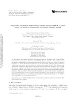
Fig. 5. Extinction ratio at the three output ports as the wavelength band: (a) 1550 nm
and (b) 1310 nm.
operation state, Phigh and Plow are output power levels in ON and OFF
states of input port respectively.
The results presented in Table 2 show that almost all important
parameters of the proposed structure such as insertion loss, cross-talk,
extinction ratio, etc. can be obtained. Crosstalk is the ratio between the
power at a specific output port from the desired input port and the
output powers from all other input ports [13].
By using the BPM, we calculate the insertion loss and cross-talk of
the switch at two wavelengths 1550 nm and 1310 nm as shown in
Fig. 4. The −2 dB bandwidths of the spectral responses at output ports
from input ports of insertion loss are 5 nm and 6 nm; the crosstalk in
these cases are from −10 dB to −15 dB, respectively.
Fig. 5 shows the spectral responses of the extinction ratios of the
switch. It can be seen that the extinction ratio of the proposed structure
are quite good. The extinction ratios at two wavelengths 1550 nm
(Fig. 5a) and 1310 nm (Fig. 5b) are −25 dB and −35 dB, respectively.
The proposed switch has an ability to switch non-blocking from any
input ports to any output ports. In comparison with an existing 3×3
optical switch using a 3×3 fiber coupler [2], we can see that the 3×3
fiber coupler cannot switch non-blocking between input and output
ports despite having phase shift in each input port. Compared with the
existing approach structure in the literature which used the 3×3 Mach
Zehnder interferometer structure and electro-optic effect [14,15], our
proposed structure has a better insertion loss and can work in all-
152