Bài giảng Điện tử công suất: Các linh kiện bán dẫn (p1) - PGS.TS Lê Minh Phương
Bạn đang xem bản rút gọn của tài liệu. Xem và tải ngay bản đầy đủ của tài liệu tại đây (1.34 MB, 19 trang )
1/21/2013
Ho Chi Minh City University of
Technology
PGS.TS Lê Minh Phương
Khoa Điện –Điện Tử
Trường Đại Học Bách Khoa
TP HỒ CHÍ MINH
Contact info:
Address: 268 Lý Thường Kiệt, P.14,Q.10, TP Hồ Chí Minh
Telephone: 84-08-38647256 (5722)
Mobile: 0988572177
E-mail: ;
1
Power Electronics
ĐIỆN TỬ CÔNG SUẤT
PGS.TS Lê Minh Phương
Khoa Điện –Điện Tử
Trường ĐHBK TPHCM
TPHCM
2012
2
1
1/21/2013
Contents – Nội dung
1. Tổng quan về Điện tử công suất
2. Các linh kiện bán dẫn
3. Mô phỏng Matlab-Simulink
4. Bộ chỉnh lưu
5. Bộ biến đổi điện áp xoay chiều
6. Bộ biến đổi điện áp một chiều
7. Bộ nghịch lưu –biến tần
1/21/2013
PGS.TS Le Minh Phuong
3
References
1. MÔ PHỎNG ĐIỆN TỬ CÔNG SUẤT TRONG
MATLAB/SIMULINK - Lê Minh Phương, Phan
Quốc Dũng – Nhà xuất bản ĐHQG 2011
2. POWER ELECTRONICS HANDBOOK –
Muhammad H. Rashid
3. MATLAB/SIMULINK - Mathworks.
/>4. ĐIỆN TỬ CÔNG SUẤT 1 – Nguyễn Văn Nhờ
Nhà xuất bản ĐHQG
1/21/2013
PGS.TS Le Minh Phuong
4
2
1/21/2013
Power Electronics
Chương 2
CÁC LINH KIỆN BÁN DẪN
PGS.TS Lê Minh Phương
Khoa Điện –Điện Tử
Trường ĐHBK TPHCM
TPHCM
2012
5
Contents – Nội dung
1. Diodes
2. Bipolar Junction Transistor (BJT)
3. Metal Oxide Semiconductor Effect Transistor
(MOSFET)
4. Insulated Gate Bipolar Transistor (IGBT)
5. Thyristor
6. Gate Turn Of Thyrisor (GTO)
7. Triode Alternative Current (TRIAC)
1/21/2013
PGS.TS Le Minh Phuong
6
3
1/21/2013
Power Electronic Devices
Các linh kiện bán dẫn cơ bản
1/21/2013
PGS.TS Le Minh Phuong
7
Power Electronic Devices
Đặc điểm:
Chỉ làm việc ở chế độ đóng ngắt switching (Đóng –Ngắt)
Khi đóng (ON):
Cho dòng điện lớn nhất chạy qua
Điện áp trên linh kiện nhỏ (Vf 0).
Điện trở Rf 0
Khi ngắt (OFF):
Dòng điện thuận If =0
Điện trở Rr
1/21/2013
PGS.TS Le Minh Phuong
8
4
1/21/2013
Power Electronic Devices
So sánh công suất các linh kiện bán dẫn
1/21/2013
PGS.TS Le Minh Phuong
9
Power Electronic Devices
The PN Junction
1/21/2013
Metallurgical
SteadyCharge
State Junction:
Space
Region - Depletion region (vùng hiếm).
Na
& Nd:
The
interface
where
the pn-type and
materials
When
no external
source
isand
connected
to the
pn meet.
junction,
diffusion
This
region
includes
positively
negatively
charged
regions.
Vùng mang điện tích the
âm net
và điện
tích dương.
10
(khuyếch
tán)
and
drift
(tái
kết)
balance
each
other
out for both the
The
space
charge
region
does
not
have
any
free
carriers.
PGS.TS Le Minh Phuong
holes and electrons
5
1/21/2013
Power Electronic Devices
Diodes
Diode là linh kiện bán dẫn không điều khiển có cấu tạo đơn giản nhất,
gồm một lớp tiếp xúc p-n, gồm 2 điện cực Anode (A) và K (Cathode)
The diode is designed to allow current to flow in only one direction. The
perfect diode would be a perfect conductor in one direction (forward
bias) and a perfect insulator in the other direction (reverse bias).In many
situations, using the ideal diode approximation is acceptable.
1/21/2013
11
PGS.TS Le Minh Phuong
Power Electronic Devices
Diodes
When an external voltage is applied, the p-n junction is considered
biased. There are two types of biasing: Forward bias and Reverse bias.
1/21/2013
Forward Bias -Phân cực
thuận,(UAK>Vf):
When the applied voltage increases,
current
to flow
across the junction.
PGS.TSstarts
Le Minh
Phuong
12
6
1/21/2013
Power Electronic Devices
Diodes
Reverse Bias -Phân cực ngược, UAK<0:
Diode ngắt: Chỉ có một số ít điện tử từ vùng p dịch chuyển qua vùng
tiếp xúc, một phần kết hợp với phần tử mang điện lỗ hổng phần còn lại
qua vùng n tới cực dương của nguồn, tạo ra dòng điện rò (leakage
currrent). Khi số tất cả các phần tử mang điện dịch chuyển hết thì dòng
giảm về 0.
1/21/2013
13
PGS.TS Le Minh Phuong
Power Electronic Devices
Đặc tính V-A
VD = Bias Voltage
ID = Current
through Diode
Ileakage = Dòng rò
VBR = Breakdown
Voltage
Vf = Barrier
Potential Voltage
1/21/2013
PGS.TS Le Minh Phuong
14
7
1/21/2013
Power Electronic Devices
Đặc tính động
Thời gian đóng diode Forward recovery time tFR:
Thời gian cần thiết để diode
có thể dòng qua diode tăng
đến giá trị xác lập khi điện
áp thuận đặt trên hai đầu
cực của diode
Thời gian phục hồi tính
nghịch
–
Reverse
Revecovery Time tRR:
Thời gian cần thiết để diode
phục hồi khả năng chịu áp
khoá khi quá trình dẫn thuận
chấm dứt
1/21/2013
PGS.TS Le Minh Phuong
t RR t a t b
15
Power Electronic Devices
Các dạng diode
Silicon rectifier diode – diode chỉnh lưu
- Có khả năng mang dòng điện lớn.
- Điện trở thuận nhỏ (m) và điện trở ngược lớn (M)
- Ứng dụng trong Power supplies, UPS, rectifiers/inverters,…
1/21/2013
PGS.TS Le Minh Phuong
16
8
1/21/2013
Power Electronic Devices
Các dạng diode
Small signal diode:
- Có ứng dụng rộng rãi nhất
- Ứng dụng trong các mạch như : switch in rectifiers, limiters,
capacitors, mạch tạo tín hiệu
1/21/2013
PGS.TS Le Minh Phuong
17
Power Electronic Devices
Schottky Diodes:
- These diodes are designed to have a very fast switching time which
makes them a great diode for digital circuit applications.
- They are very common in computers because of their ability to be
switched on and off so quickly.
1/21/2013
PGS.TS Le Minh Phuong
18
9
1/21/2013
Power Electronic Devices
Zener diode:
- Ứng dụng chính là tạo điện áp tham chiếu và điều chỉnh
- Khả năng duy trì điện áp phụ thuộc vào hệ số nhiệt độ và điện trở
1/21/2013
PGS.TS Le Minh Phuong
19
Power Electronic Devices
Photo diode:
- Khi tiếp xúc (junction) bị tác động của ánh sáng, các photon tạo ra
điện tích lỗ hổng và tạo ra photocurrent nhờ quá trình dịch chuyển.
-Photo-diode hoạt động như một nguồn dòng, và tăng khi cường độ
ánh sáng tăng.
1/21/2013
PGS.TS Le Minh Phuong
20
10
1/21/2013
Power Electronic Devices
Light emitting diode (LED):
Light-emitting diodes được thiết kế với vùng dịch chuyển lớn sao cho
các hạt khi qua vùng nghèo (depletion region) sẽ tạo ra photon ánh
sáng. LED với vùng dịch chuyển năng lượng cao sẽ tạo ra ánh sáng
nhìn thấy. LED với vùng dịch chuyển năng lượng cao sẽ tạo ra ánh
sáng . LED với vùng dịch chuyển năng lượng thấpsẽ phát ra bức xạ
hồng ngoại
1/21/2013
PGS.TS Le Minh Phuong
21
Power Electronic Devices
Typical Diode Ratings
Voltage Ratings:
Repetitive peak inverse voltage (VRRM ):
The non-repetitive voltage (VRM): khả năng chịu điện áp ngược
Current Ratings
The datasheet of a diode normally specifies three different current
ratings:
(1) the average current,
(2) the rms current, and
(3) the peak current.
1/21/2013
PGS.TS Le Minh Phuong
23
11
1/21/2013
Power Electronic Devices
Typical
Diode
Ratings
1/21/2013
PGS.TS Le Minh Phuong
24
Power Electronic Devices
Snubber Circuits for Diode
Snubber circuits cần thiết khi diode chuyển mạch, nó giúp bảo vệ
diode khỏi quá điện áp phát sinh trong quá trình are essential for
diodes used in switching reverse recovery
1/21/2013
PGS.TS Le Minh Phuong
25
12
1/21/2013
Power Electronic Devices
Typical Applications of Diodes
1/21/2013
PGS.TS Le Minh Phuong
26
Power Electronic Devices
Typical Applications of Diodes
1. Dùng trong mạch chỉnh lưu
1/21/2013
PGS.TS Le Minh Phuong
27
13
1/21/2013
Power Electronic Devices
Typical Applications of Diodes
1. Dùng trong mạch chỉnh lưu
1/21/2013
PGS.TS Le Minh Phuong
28
Power Electronic Devices
Power Bipolar Transistors (BJT)
The bipolar junction transistor (BJT) consists of a three-region
structure of n-type and p-type semiconductor materials, it can be
constructed as npn as well as pnp.
Gồm 3 điện cực Collector (C), Emitter (E) và Base (B).
Mạch công suất nối giữa C-E, mạch điều khiển nối giữa cổng B-E.
Tồn tại hai dạng BJT: n-p-n và p-n-p.
BJT là linh kiện bán dẫn điều khiển đóng ngắt hoàn toàn bằng
dòng điện.
1/21/2013
PGS.TS Le Minh Phuong
31
14
1/21/2013
Power Electronic Devices
Power Bipolar Transistors (BJT)
1/21/2013
PGS.TS Le Minh Phuong
32
Power Electronic Devices
The NPN Transistor
1/21/2013
PGS.TS Le Minh Phuong
38
15
1/21/2013
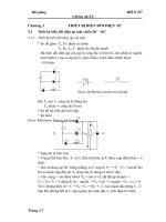
Power Electronic Devices
Nguyên lý làm việc
C
IC
n
IB
p
holes
n
electrons
UCE
holes
B
E
1/21/2013
Khi VBE>0 lớp tiếp xúc p-n giữa Base và
Emiter phân cực thuận, nhờ đó điện tử
dịch chuyển từ Emiter đến Base. Vì
vùng Base có cấu trúc rất mỏng nên chỉ
có một phần nhỏ điện tử kết hợp với
điện tích dương ở vùng này.
Lúc này VCE>0 nên Phần lớn điện tử sẽ
chạy đến vùng phân cực ngược Base –
Collector và tới cực Collector làm BJT
dẫn.
Trạng thái đóng ngắt
UCE>0, IB>0 BJT đóng (dẫn)
UCE>0 ,IB<=0 BJT ngắt
40
PGS.TS Le Minh Phuong
Power Electronic Devices
Đặc tính V-A
1. Cut-off Region
Here the operating
2.
Active region
conditions
of the –
Constant
current
transistor are
zero
The
activecurrent
region (IisB),
input base
horizontal
of
3. Saturation
zero
outputportion
collector
curves
. (IItCshows
current
) and
Region
“constant”
Ctransistor
current,
maximum
Here theicollector
because
the
collector
voltage
(V
will be biased
CE ). so: the
current
does
not is
Therefore
the
collector
current
change
significantly
with
transistor
isinswitched
maximum
the
V"Fully-OFF".
CE for a given
iB.
minimum
collector
Those
portionsdrop.
are
emitter voltage
used
only for the
small
Therefore
signal
transistor
transistor
is switched
operating
as linear
"Fully-ON".
amplifiers
1/21/2013
PGS.TS Le Minh Phuong
41
16
1/21/2013
Power Electronic Devices
The Transistor as a Switch
1. Cut-off Region
Then we can define the "cut-off region" or "OFF
mode" when using a bipolar transistor as a
switch as being, both junctions reverse biased,
UBE < 0.7V and IC = 0.
Base-Emitter voltage VBE < 0.7V
Base-Emitter junction is reverse
Base-Collector junction is reverse
No Collector current flows (IC = 0)
VOUT = VCE = VCC = "1”
Transistor is "fully-OFF" (Cut-off
region)
1/21/2013
43
PGS.TS Le Minh Phuong
Power Electronic Devices
The Transistor as a Switch
2. Saturation Region
Then we can define the "saturation region" or
"ON mode" when using a bipolar transistor as a
switch as being, both junctions forward biased,
UBE > 0.7V and IC = Maximum
The input and Base are connected to VCC
Base-Emitter voltage VBE > 0.7V
Base-Emitter junction is forward biased
Base-Collector junction is forward biased
Transistor is "fully-ON" (saturation region)
Max Collector current flows (IC = Vcc/RL)
VCE = 0 (ideal saturation)
VOUT = VCE = "0"
Transistor operates as a "closed switch"
1/21/2013
PGS.TS Le Minh Phuong
44
17
1/21/2013
Power Electronic Devices
The Transistor as a Switch
1/21/2013
45
PGS.TS Le Minh Phuong
Power Electronic Devices
Dynamic Switching Characteristics
1/21/2013
PGS.TS Le Minh Phuong
td
thời gian trễ đóng
tr
thời gian tăng dòng
ton=td+tr
thời gian đóng
ts
Thời gian trễ ngắt
tf
Thời gian giảm dòng
Toff=ts+tf
thời gian ngắt
46
18
1/21/2013
Power Electronics
For Building
THANK YOU
FOR YOUR ATTENTION
1/21/2013
58
19