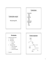
Lecture Digital logic design - Lecture 10: Circuit analysis procedure
Bạn đang xem bản rút gọn của tài liệu. Xem và tải ngay bản đầy đủ của tài liệu tại đây (664 KB, 39 trang )
Lecture 10
Circuit Analysis Procedure
1
Overvie
w
° Hazards
• Glitches
° Important concept – analyze digital circuits
• Given a circuit
- Create a truth table
-
Create a minimized circuit
° Approaches
• Boolean expression approach
• Truth table approach
° Leads to minimized hardware
° Provides insights on how to design hardware
2
Gate Delays
° When the input to a logic gate is changed, the
output will not change immediately.
° The switching elements within a gate take a finite
time to react to a change (transition) in input.
° As a result the change in the gate output is delayed
w.r.t. to the input change.
° Such delay is called the propagation delay of the
logic gate (tp)
° The propagation delay for a 0 to 1 output change
(tpLH) may be different than the delay for a 1 to 0
change (tpHL).
3
Gat
e
Del
ays
(co
nt’d
)
Digital signal:
4
Important Terms (timing)
° Gate delay — time for change at input to cause
change at output
• min delay – typical/nominal delay – max
delay
• careful designers design for both worst case
and best case
° Rise time — time for output to transition from
low to high voltage
° Fall time — time for output to transition from
high to low voltage
° Pulse width — time that an output stays high or
stays low between changes
5
Effect of gate delays
° The analysis of combinational circuits ignoring
delays can predict only the steady-state behavior of
a circuits.
That is they predict a circuit’s output as a function
of its inputs under the assumption that the inputs
have been stable for a long time, relative to the
delays into the circuit’s electronics.
° Because of circuit delays, the transient behavior of
a combinational logic circuit may differ from what
is predicted by a steady-state analysis.
° In particular a circuit’s output may produce a short
pulse (often called a glitch) at a time when steady
state analysis predicts that the output should not
change.
6
Hazards and Glitches
° A glitch is an unwanted pulse at the output of a
combinational logic network – a momentary change
in an output that should not have changed.
° A circuit with the potential for a glitch is said to
have a hazard.
° In other words a hazard is something intrinsic
about a circuit; a circuit with hazard may or may
not have a glitch depending on input patterns and
the electric characteristics of the circuit.
When do circuits have hazards ?
° Hazards are potential unwanted transients that
occur in the output when different paths from input
to output have different propagation delays.
7
Circuit Analysis
Analyze a logic circuit to determine its behavior.
For a two-level circuit, the analysis
process is simple.
Boolean expression can often be written by
inspection.
For multi-level circuits, the process is
more complex.
Cannot write a Boolean expression by
inspection.
Must follow a procedure to implement the
analysis.
8
Relationship Among Representations
Any Boolean function that can be expressed as a truth table
can be written as an expression in Boolean Algebra using
AND, OR, NOT.
?
not
u n iq u e
B o o le a n
E x p r e s s io n
[ c o n v e n ie n t f o r
m a n ip u la tio n ]
u n iq u e
T r u th T a b le
?
g a te
r e p r e s e n ta tio n
(s c h e m a tic )
not
u n iq u e
[ c lo s e to
im p le m e n ta to n ]
How do we convert from one to the other?
9
Logic circuits
° Logic circuits for digital systems may be
combinational or sequential.
° Combinational circuit consists of logic gates whose
outputs at any time are determined directly from
the present combination of inputs without regard to
previous inputs.
° Combinational circuit performs a specific
information-processing operation fully specified
logically by a set of Boolean functions.
10
Sequential circuits
° Sequential circuits employ memory
elements (binary cells) in addition to logic
gates.
° Their outputs are a function of the inputs
and the state of the memory elements.
• The state of memory elements, in turn, is a
function of previous inputs.
° As a consequence, the outputs of a
sequential circuit depend not only on
present inputs, but also on past inputs,
• the circuit behavior must be specified by a time
sequence of inputs and internal states.
11
Basic Combinational Logic Circuits
° AND-OR logic
• AND-OR logic produces an
SOP expression.
• In general, an AND-OR circuit
can have any number of AND
gates each with any number of
inputs.
A
B
AB
SOP
X=AB+CD
C
D
CD
12
Basic Combinational Logic Circuits
inputs
o/p
AB
A
B
AB
X=AB+CD
C
D
CD
CD
A
B
C
D
X
0
0
0
0
0
0
0
0
0
0
1
0
0
0
0
0
1
0
0
0
0
0
0
1
1
0
1
1
0
1
0
0
0
0
0
0
1
0
1
0
0
0
0
1
1
0
0
0
0
0
1
1
1
0
1
1
1
0
0
0
0
0
0
1
0
0
1
0
0
0
1
0
1
0
0
0
0
1
0
1
1
0
1
1
1
1
0
0
1
0
1
1
1
0
1
1
0
1
1
1
1
0
1
0
1
1
1
1
1
1
1
1
13
Combinational circuit
° A combinational circuit consists of:
•
input variables,
• logic gates,
• output variables.
° The logic gates accept signals from the inputs and
generate signals to the outputs.
° This process transforms binary information from
the given input data to the required output data.
•
Obviously, both input and output data are represented by binary
signals,
14
Co
mbi
°nati
Combinational circuits -- outputs depend only on
ona
current inputs (not on history).
l°Circ
Kinds of combinational analysis:
uit • exhaustive (truth table)
Ana
• algebraic (expressions)
lysi• simulation / test bench
s
- Write functional description in HDL
-
Define test conditions / test vectors, including corner
cases
-
Compare circuit output with functional description (or
known-good realization)
-
Repeat for “random” test vectors
15
Co
mbi
°nati
Sometimes you can write an equation or equations
ona
directly using “logic” (the kind in your brain).
l°Circ
Example (alarm circuit):
uit
Des
ign
° Corresponding circuit:
16
Alar
m°circ
Sum-of-products form
uit
• Useful for programmable logic devices (next lec.)
tran
sfor
mati
°on
“Multiply out”:
17
The Problem
° How can we convert from a circuit drawing to an
equation or truth table?
° Two approaches
° Create intermediate equations
° Create intermediate truth tables
A
B
C
Out
A
B
C’
18
Label Gate Outputs
1. Label all gate outputs that are a function of input
variables.
2. Label gates that are a function of input variables
and previously labeled gates.
3. Repeat process until all outputs are labelled.
A
B
C
A
B
R
S
T
Out
C’
By repeated substitution of previously defined
functions, obtain the output Boolean functions
in terms of input variables.
19
Approach 1: Create Intermediate Equations
Step 1: Create an equation for each gate output based
on its input.
•
R = ABC
•
S=A+B
•
T = C’S
•
Out = R + T
A
B
C
A
R
S
T
Out
B
C’
20
Approach 1: Substitute in subexpressions
Step 2: Form a relationship based on input variables
(A, B, C)
•
R = ABC
•
S=A+B
•
T = C’S = C’(A + B)
•
Out = R+T = ABC + C’(A+B)
A
B
C
A
R
S
T
Out
B
C’
21
Approach 1: Substitute in subexpressions
Step 3: Expand equation to SOP final result
•
Out = ABC + C’(A+B) = ABC + AC’ + BC’
A
B
C
Out
A
C’
B
C’
22
Approach 2: Truth Table
Step 1: Determine outputs for functions of input
variables.
A B C R S
0 0 0 0 0
0 0 1 0 0
0 1 0 0 1
0 1 1 0 1
1 0 0 0 1
1 0 1 0 1
1 1 0 0 1
1 1 1 1 1
A
R
B
C
A
S
T
Out
B
C’
23
Approach 2: Truth Table
Step 2: Determine outputs for functions of
intermediate variables.
A B C C’ R S
0 0 0 1 0 0
T = S * C’
0 0 1 0 0 0
0 1 0 1 0 1
0 1 1 0 0 1
1 0 0 1 0 1
1 0 1 0 0 1
1 1 0 1 0 1
1 1 1 0 1 1
A
R
B
C
A
S
T
T
0
0
1
0
1
0
1
0
Out
B
C’
24
Approach 2: Truth Table
Step 3: Determine outputs for function.
R + T = Out
A
B
C
A
R
S
A
0
0
0
0
1
1
1
1
T
B
0
0
1
1
0
0
1
1
C
0
1
0
1
0
1
0
1
R
0
0
0
0
0
0
0
1
S
0
0
1
1
1
1
1
1
T
0
0
1
0
1
0
1
0
Out
0
0
1
0
1
0
1
1
Out
B
C’
25